EP0597664B1 - X-ray mirror and material - Google Patents
X-ray mirror and material Download PDFInfo
- Publication number
- EP0597664B1 EP0597664B1 EP93308928A EP93308928A EP0597664B1 EP 0597664 B1 EP0597664 B1 EP 0597664B1 EP 93308928 A EP93308928 A EP 93308928A EP 93308928 A EP93308928 A EP 93308928A EP 0597664 B1 EP0597664 B1 EP 0597664B1
- Authority
- EP
- European Patent Office
- Prior art keywords
- film
- ray
- mirror
- reflecting
- density
- Prior art date
- Legal status (The legal status is an assumption and is not a legal conclusion. Google has not performed a legal analysis and makes no representation as to the accuracy of the status listed.)
- Expired - Lifetime
Links
Images

Classifications
-
- G—PHYSICS
- G21—NUCLEAR PHYSICS; NUCLEAR ENGINEERING
- G21K—TECHNIQUES FOR HANDLING PARTICLES OR IONISING RADIATION NOT OTHERWISE PROVIDED FOR; IRRADIATION DEVICES; GAMMA RAY OR X-RAY MICROSCOPES
- G21K1/00—Arrangements for handling particles or ionising radiation, e.g. focusing or moderating
- G21K1/06—Arrangements for handling particles or ionising radiation, e.g. focusing or moderating using diffraction, refraction or reflection, e.g. monochromators
-
- G—PHYSICS
- G21—NUCLEAR PHYSICS; NUCLEAR ENGINEERING
- G21K—TECHNIQUES FOR HANDLING PARTICLES OR IONISING RADIATION NOT OTHERWISE PROVIDED FOR; IRRADIATION DEVICES; GAMMA RAY OR X-RAY MICROSCOPES
- G21K2201/00—Arrangements for handling radiation or particles
- G21K2201/06—Arrangements for handling radiation or particles using diffractive, refractive or reflecting elements
Definitions
- the present invention relates to an x-ray mirror and material and in particular to, but not exclusively to, a total reflection mirror and a multilayer mirror for use with x-ray radiation.
- a total reflecting mirror, a multilayer mirror, and so on are used depending on the use and the particular wave length. If an oblique incident angle is small, the mirror of the catoptric system increases in area. On the other hand, the area of an optical system for focusing and an imaging mirror reduces in aperture and thereby increases in aberration. Therefore, it is preferable to ensure that a critical angle between incident x-rays and the mirror surface for total reflection is large.
- a reflecting material is important because the critical angle of total reflection is proportional to a density of the reflecting material.
- a high density substance such as gold (Au) and platinum (Pt) is often used.
- Au and Pt are chemically quite stable and thereby utilised for the reflecting surface in addition to their excellent reflecting properties.
- material such as Au and Pt, are deposited on a surface of material, such as quartz glass, single silicon, and SiC, which can be polished to obtain a very level surface, by physical or chemical vapour deposition, such as vacuum deposition and sputtering or plating.
- Such mirrors are for instance known from JP-A-63266398 or JP-A-1309000.
- An x-ray has a relatively short wave length, which is about 1/10-1/1000 of that of visible light. So in order to obtain highly efficient reflectance in this wave length region, the roughness of the reflecting surface and the interface must be reduced to about 1/10-1/1000 of that of visible light. Also, when using a substrate, such as quartz glass, which is polished level, the roughness of the film surface can increase at deposition. Particularly, substances such as Pt and Au, have a low Debye temperature and so the mobility of the atoms at room temperature is large. As a result, the crystal grains grow during vacuum deposition and sputtering which results in the roughness of the surface increasing.
- a film which is 10-100 x 10 -9 m (100-1000 ⁇ ) thick is deposited to form a total reflecting mirror.
- the film thickness of one layer constituting a multilayer mirror is between 1 and 10 x 10 -9 m (10 ⁇ and 100 ⁇ ). If the film is formed by the above-mentioned method, the density of the film is inclined to reduce by about 5-30% as compared to that of a bulk material within the above film thickness. Therefore, a sufficient x-ray reflecting performance cannot be obtained.
- An object of the present invention is to reduce the surface roughness of a film formed by the above deposition method and provide a reflecting material for an x-ray mirror which has almost equal density to a pure film and which is superior in reflecting properties and is further chemically stable.
- an x-ray mirror for reflecting x-ray radiation comprising, a reflecting material formed on a substrate and comprising Pt and characterised by a material chosen from Mo, Ru, Rh, Pd, Ta, W and Au.
- the present invention uses an alloy film expressed as a general formula Pt 1-x M x , for a mirror surface of an x-ray mirror so as to reduce the surface roughness without reducing the film density so much.
- M may be selected from one or more of the following substances; Mo, Ru, Rh, Pd, Ta, W and Au. x, in order to satisfy the equation; should fall in the range 0.005 ⁇ x ⁇ 0.10. If x is indicated by percentage, x should fall between 0.5% and 10% and the formula is expressed as Pt 100-x M x .
- the crystal grain size of an alloy film according to the present invention gets much smaller than that of a conventional pure Pt film. Further, dispersion of the crystal grain size reduces and besides the surface roughness reduces. Thus the film density does not decline so much, since the quantity of additions is small. Hence, the x-ray reflecting performance is improved. If the additions are added at more than 10% the surface roughness deteriorates and the film density also deteriorates. Consequently the x-ray reflecting performance declines.
- a Pt-Pd film used for an x-ray mirror material of the present invention can be deposited in the following method. Deposition is performed by sputtering. However, many other deposition techniques can be also utilised. When sputtering is performed, the substrate temperature is kept at almost room temperature.
- both single silicon and BK7 glass are employed as a substrate.
- any other materials which can be polished to be very level, can be also used.
- This embodiment discloses a Pt-Pd film in a total reflecting mirror which is used for the x-ray wave length region of 0.07 to 0.02 x 10 -9 m (0.7-2 ⁇ ).
- a target a composite target in which a Pd chip is disposed on a Pt target is used so as to control precisely the quantity of Pd.
- the film thickness of the Pt-Pd alloy film is approximately 50 x 10 -9 m (500 ⁇ ).
- Pd content is adjusted between 1 atomic percent and 10 atomic percent.
- the crystal grain size of a pure Pt film is between 10 and 50 x 10 -9 m (100 ⁇ and 500 ⁇ ) and each crystal grain size varies differently.
- the size is 20 x 10 -9 m (200 ⁇ ) on average.
- the crystal grain size of the Pt-Pd alloy film, to which Pd is added at 1-2 atomic percent is between 5 and 15 x 10 -9 m (50 ⁇ and 150 ⁇ ). That is to say, a pretty small crystal grain size can be obtained. Further, the dispersion of the crystal grain size can be suppressed.
- the crystal grain size is about 9 x 10 -9 m (90 ⁇ ) on average.
- the upper limit of Pd is 10 atomic percent for suppressing the dispersion and reducing the crystal grain size.
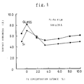
- Figure 1 is a graph showing the relationship between the quantity of Pd and a rms (root mean square) of the surface roughness. Adding Pd reduces considerably the surface roughness as compared to a pure Pt sputtering film. The same effect can be obtained in single silicon and a BK7 glass substrate.
- the Pd content at which the surface roughness of the Pt-Pd alloy film becomes a minimum, is 3-4 atomic percent.
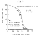
- Figure 2 is a graph showing the x-ray reflectance measured against a CuK ⁇ x-ray (i.e., one whose wave length is 0.154 x 10 -9 (1.54 ⁇ ).
- the x-ray reflectance which is actually measured is smaller than the theoretical reflectance. This is due to the surface roughness and a low density of the Pt film, which is lower than that of the bulk state Pt.
- Most of Pt-Pd alloy films to which Pd is added, can obtain a higher reflectance than that of a pure Pt film at an oblique incidence angle of less than 0.5°.
- an x-ray multilayer mirror having high reflectance can be produced utilising an alloy film expressed as the general formula; Pt 1-x M x .
- M represents one or more substances of Mo, Rh, Pd, Ta, W and Au, and further, x satisfies the following formula 0.005 ⁇ x ⁇ 0.10.
- the x-ray multilayer mirror is constituted of the combination of a high density metal and low density material, wherein approximately 10-200 layers are laminated and each layer has the thickness of 1-10 x 10 -9 m (10-100 ⁇ ),
- the x-ray multilayer mirror is produced by vacuum deposition.
- the following two multilayered films are produced.
- One is comprised of Pt and carbon, C; the other is comprised of Pt containing Pd at 1 atomic percent and C.
- the thickness of one layer is 2.5 x 10 -9 m (25 ⁇ ).
- Figure 3 is a graph showing x-ray reflectance of a Pt/C x-ray multilayer mirror and Pt containing Pd at 1 atomic percent/C.
- the x-ray multilayer mirror is measured with an AIK ⁇ x-ray having a wave length of 0.834 x 10 -9 m (8.34 ⁇ ).
- the peak x-ray reflectance is between 2% and 3 %.
- the theoretical reflectance of the Pt/C x-ray multilayer mirror is 32%. The difference with ideal reflectance is caused by the roughness of the surface and the interface and the decline of film density.
- the rms surface roughness and the interface roughness is between 0.45 and 0.55 x 10 -9 m (4.5 ⁇ and 5.5 ⁇ ) and that the film density of Pt and C is approximately 80% of the density in a bulk state.
- the alloy film is expressed as the general formula Pt 1-x M x and constitutes one element of a combination constituting a multilayered film.
- the M represents one or more substances of Mo, Ru, Rh, Pd, Ta, W, and Au, and X satisfies the formula: 0.005 ⁇ x ⁇ 0.10.
- the crystal grain is miniaturised in order to reduce the surface roughness.
- an alloyed amorphous film is employed for reducing the surface roughness.
- a diffraction peak to an x-ray cannot be seen in an alloy film expressed as the general formula Pt 1-x M x so that the above alloy film is an amorphous film.
- the M represents one or more substances of Mo, Rh, Ta, and W, and X satisfies the formula 0.10 ⁇ x ⁇ 0.20.
- the alloy film used for a reflecting surface of an x-ray mirror expressed as a general formula Pt 1-x M x can reduce the roughness of the surface and the interface but hardly reduces the density.
- the present invention can provide a stable reflecting material for an x-ray mirror.
- M represents one or more substances of Mo, Ru, Rh, Pd, Ta, W, and Au, and X satisfies the formula 0.005 ⁇ x ⁇ 0.10.
Description
- The present invention relates to an x-ray mirror and material and in particular to, but not exclusively to, a total reflection mirror and a multilayer mirror for use with x-ray radiation.
- In a catoptric system wherein radiation having a wave length in an x-ray region, 0.01 to 20 x 10-9m (0.1 to 200 Å), is employed, a total reflecting mirror, a multilayer mirror, and so on are used depending on the use and the particular wave length. If an oblique incident angle is small, the mirror of the catoptric system increases in area. On the other hand, the area of an optical system for focusing and an imaging mirror reduces in aperture and thereby increases in aberration. Therefore, it is preferable to ensure that a critical angle between incident x-rays and the mirror surface for total reflection is large.
- A reflecting material is important because the critical angle of total reflection is proportional to a density of the reflecting material. Thus, a high density substance, such as gold (Au) and platinum (Pt) is often used. Au and Pt are chemically quite stable and thereby utilised for the reflecting surface in addition to their excellent reflecting properties. In these reflecting mirrors, material such as Au and Pt, are deposited on a surface of material, such as quartz glass, single silicon, and SiC, which can be polished to obtain a very level surface, by physical or chemical vapour deposition, such as vacuum deposition and sputtering or plating. Such mirrors are for instance known from JP-A-63266398 or JP-A-1309000.
- An x-ray has a relatively short wave length, which is about 1/10-1/1000 of that of visible light. So in order to obtain highly efficient reflectance in this wave length region, the roughness of the reflecting surface and the interface must be reduced to about 1/10-1/1000 of that of visible light. Also, when using a substrate, such as quartz glass, which is polished level, the roughness of the film surface can increase at deposition. Particularly, substances such as Pt and Au, have a low Debye temperature and so the mobility of the atoms at room temperature is large. As a result, the crystal grains grow during vacuum deposition and sputtering which results in the roughness of the surface increasing.
- Moreover, a film which is 10-100 x 10-9m (100-1000 Å) thick is deposited to form a total reflecting mirror. The film thickness of one layer constituting a multilayer mirror is between 1 and 10 x 10-9m (10 Å and 100 Å). If the film is formed by the above-mentioned method, the density of the film is inclined to reduce by about 5-30% as compared to that of a bulk material within the above film thickness. Therefore, a sufficient x-ray reflecting performance cannot be obtained.
- An object of the present invention is to reduce the surface roughness of a film formed by the above deposition method and provide a reflecting material for an x-ray mirror which has almost equal density to a pure film and which is superior in reflecting properties and is further chemically stable.
- According to the present invention, there is provided an x-ray mirror for reflecting x-ray radiation comprising, a reflecting material formed on a substrate and comprising Pt and characterised by a material chosen from Mo, Ru, Rh, Pd, Ta, W and Au.
- Also, the present invention uses an alloy film expressed as a general formula Pt1-x Mx, for a mirror surface of an x-ray mirror so as to reduce the surface roughness without reducing the film density so much.
- M may be selected from one or more of the following substances; Mo, Ru, Rh, Pd, Ta, W and Au. x, in order to satisfy the equation; should fall in the range 0.005 ≤ x ≤ 0.10. If x is indicated by percentage, x should fall between 0.5% and 10% and the formula is expressed as Pt100-x Mx.
- When the above-described additions to the Pt material of 0.5-10%, the crystal grain size of an alloy film according to the present invention gets much smaller than that of a conventional pure Pt film. Further, dispersion of the crystal grain size reduces and besides the surface roughness reduces. Thus the film density does not decline so much, since the quantity of additions is small. Hence, the x-ray reflecting performance is improved. If the additions are added at more than 10% the surface roughness deteriorates and the film density also deteriorates. Consequently the x-ray reflecting performance declines.
- Embodiments of the present invention will now be described with reference to the accompanying drawings, of which:
- Figure 1 is a graph showing the relationship between the surface roughness and the concentration of M in the inventive alloy film when M comprises Pd, both on a glass substrate and a Si substrate;
- Figure 2 is a graph giving the x-ray reflectance of the inventive alloy film against the CuK α x-ray incident angle when the film comprises Pt-Pd; and
- Figure 3 is a graph showing the x-ray reflectance against the incident angle of the multilayered x-ray mirror comprising a combination of the inventive Pt-Pd alloy film and a carbon film.
- Hereinafter, the present invention will be described with reference to the preferred embodiments.
- A Pt-Pd film used for an x-ray mirror material of the present invention can be deposited in the following method. Deposition is performed by sputtering. However, many other deposition techniques can be also utilised. When sputtering is performed, the substrate temperature is kept at almost room temperature.
- In the present invention, both single silicon and BK7 glass are employed as a substrate. However, any other materials, which can be polished to be very level, can be also used.
- This embodiment discloses a Pt-Pd film in a total reflecting mirror which is used for the x-ray wave length region of 0.07 to 0.02 x 10⁻⁹m (0.7-2 Å). As for a target, a composite target in which a Pd chip is disposed on a Pt target is used so as to control precisely the quantity of Pd. The film thickness of the Pt-Pd alloy film is approximately 50 x 10-9m (500 Å). Pd content is adjusted between 1 atomic percent and 10 atomic percent. Conventionally, the crystal grain size of a pure Pt film is between 10 and 50 x 10-9m (100 Å and 500 Å) and each crystal grain size varies differently. The size is 20 x 10-9m (200 Å) on average. On the other hand, the crystal grain size of the Pt-Pd alloy film, to which Pd is added at 1-2 atomic percent, is between 5 and 15 x 10-9m (50 Å and 150 Å). That is to say, a pretty small crystal grain size can be obtained. Further, the dispersion of the crystal grain size can be suppressed. The crystal grain size is about 9 x 10⁻⁹m (90 Å) on average. The upper limit of Pd is 10 atomic percent for suppressing the dispersion and reducing the crystal grain size.
- Figure 1 is a graph showing the relationship between the quantity of Pd and a rms (root mean square) of the surface roughness. Adding Pd reduces considerably the surface roughness as compared to a pure Pt sputtering film. The same effect can be obtained in single silicon and a BK7 glass substrate. The Pd content at which the surface roughness of the Pt-Pd alloy film becomes a minimum, is 3-4 atomic percent.
- Figure 2 is a graph showing the x-ray reflectance measured against a CuK α x-ray (i.e., one whose wave length is 0.154 x 10⁻⁹ (1.54 Å). The curve indicated with a solid line shows the theoretical reflectance when a Pt film has an ideal surface (i.e. roughness = 0) and has a density equal to a bulk state of Pt. As shown in Figure 2, the x-ray reflectance which is actually measured, is smaller than the theoretical reflectance. This is due to the surface roughness and a low density of the Pt film, which is lower than that of the bulk state Pt. Most of Pt-Pd alloy films to which Pd is added, can obtain a higher reflectance than that of a pure Pt film at an oblique incidence angle of less than 0.5°.
- On the other hand, a critical angle of total reflection deteriorates because adding Pd at more than about 3 atomic percent reduces the density considerably. As long as Pd is added at less than 3 atomic percent, the density of the Pt-Pd film is almost the same value as a pure Pt film. Further, a high reflectance than a pure Pt film can be achieved.
- The same effect can also be achieved when using a Pt1-x Mx film and as deposited as described above, where M is another substance rather than Pd from among Mo, Ru, Rd, Ta, W.
- According to the result shown in Embodiment 1, an x-ray multilayer mirror having high reflectance can be produced utilising an alloy film expressed as the general formula; Pt1-x Mx. M represents one or more substances of Mo, Rh, Pd, Ta, W and Au, and further, x satisfies the following formula 0.005 ≤ x ≤ 0.10.
- The x-ray multilayer mirror is constituted of the combination of a high density metal and low density material, wherein approximately 10-200 layers are laminated and each layer has the thickness of 1-10 x 10-9m (10-100 Å), The x-ray multilayer mirror is produced by vacuum deposition. The following two multilayered films are produced. One is comprised of Pt and carbon, C; the other is comprised of Pt containing Pd at 1 atomic percent and C. The thickness of one layer is 2.5 x 10⁻⁹m (25 Å).
- Figure 3 is a graph showing x-ray reflectance of a Pt/C x-ray multilayer mirror and Pt containing Pd at 1 atomic percent/C. The x-ray multilayer mirror is measured with an AIK α x-ray having a wave length of 0.834 x 10⁻⁹m (8.34 Å). As shown in Figure 3, the peak x-ray reflectance is between 2% and 3 %. When a multilayered film comprising Pt and C has an ideal surface and an ideal interface (roughness = 0) and is equal to a bulk state in density, the theoretical reflectance of the Pt/C x-ray multilayer mirror is 32%. The difference with ideal reflectance is caused by the roughness of the surface and the interface and the decline of film density. In the produced multilayered film the Pt/C x-ray multilayer mirror, it can be estimated that the rms surface roughness and the interface roughness is between 0.45 and 0.55 x 10⁻⁹m (4.5 Å and 5.5 Å) and that the film density of Pt and C is approximately 80% of the density in a bulk state.
- On the other hand, in the x-ray multilayer mirror comprising the combination of Pt containing Pd at 1 atomic percent and C, peak reflectance is about 15% and the roughness of the film surface and the interface is 0.25 - 0.3 x 10⁻⁹m (2.5-3 Å). Even if the thickness of one layer of a multilayered film is between 1 and 10 x 10-9m (10 Å and 100 Å), a similar effect can be obtained on reducing the roughness of the film surface and the interface. Figure 3 shows a multilayered film comprising the combination of Pt containing Pd at 1 atomic percent and C as an example. However, a similar effect can be gained as long as the alloy film is expressed as the general formula Pt1-x Mx and constitutes one element of a combination constituting a multilayered film. The M represents one or more substances of Mo, Ru, Rh, Pd, Ta, W, and Au, and X satisfies the formula: 0.005 ≤ x ≤ 0.10.
- According to embodiment 1, the crystal grain is miniaturised in order to reduce the surface roughness. In Embodiment 3, an alloyed amorphous film is employed for reducing the surface roughness. A diffraction peak to an x-ray cannot be seen in an alloy film expressed as the general formula Pt1-x Mx so that the above alloy film is an amorphous film. The M represents one or more substances of Mo, Rh, Ta, and W, and X satisfies the formula 0.10 ≤ x ≤ 0.20.
- As described above, the alloy film used for a reflecting surface of an x-ray mirror expressed as a general formula Pt1-x Mx can reduce the roughness of the surface and the interface but hardly reduces the density. Namely, the present invention can provide a stable reflecting material for an x-ray mirror. M represents one or more substances of Mo, Ru, Rh, Pd, Ta, W, and Au, and X satisfies the formula 0.005 ≤ x ≤ 0.10.
- The aforegoing description has been given by way of example only and it will be appreciated by a person skilled in the art that modifications can be made without departing from the scope of the present claims.
Claims (5)
- An X-ray mirror for reflecting X-ray radiation, comprising a layer of reflecting alloy formed on a substrate, the reflecting alloy being characterised by the formula Pt1-xMx wherein M represents a metal chosen from Mo, Ru, Rh, Pd, Ta, W and Au and 0.005 ≤x≤ 0.10.
- An X-ray mirror according to claim 1, wherein said alloy has an average grain size of less than 15 nanometres.
- An X-ray mirror according to claim 1 or claim 2, wherein M represents Pd and x≤0.03.
- An X-ray mirror according to any preceding claim in which the X-ray mirror is a multi-layered mirror comprising alternate layers of said alloy and a low density material.
- An X-ray mirror according to claim 4, wherein said low density material is carbon.
Applications Claiming Priority (2)
| Application Number | Priority Date | Filing Date | Title |
|---|---|---|---|
| JP302556/92 | 1992-11-12 | ||
| JP4302556A JP2995371B2 (en) | 1992-11-12 | 1992-11-12 | X-ray reflector material |
Publications (3)
| Publication Number | Publication Date |
|---|---|
| EP0597664A2 EP0597664A2 (en) | 1994-05-18 |
| EP0597664A3 EP0597664A3 (en) | 1994-07-13 |
| EP0597664B1 true EP0597664B1 (en) | 1996-08-21 |
Family
ID=17910404
Family Applications (1)
| Application Number | Title | Priority Date | Filing Date |
|---|---|---|---|
| EP93308928A Expired - Lifetime EP0597664B1 (en) | 1992-11-12 | 1993-11-09 | X-ray mirror and material |
Country Status (4)
| Country | Link |
|---|---|
| US (1) | US5454021A (en) |
| EP (1) | EP0597664B1 (en) |
| JP (1) | JP2995371B2 (en) |
| DE (1) | DE69304177T2 (en) |
Families Citing this family (7)
| Publication number | Priority date | Publication date | Assignee | Title |
|---|---|---|---|---|
| JP2000338299A (en) | 1999-05-28 | 2000-12-08 | Mitsubishi Electric Corp | Device and method for exposure to x-ray, x-ray mask, x- ray mirror synchrotron radiation device, method for synchrotron radiation an semiconductor device |
| JP3766802B2 (en) * | 1999-07-22 | 2006-04-19 | コーニング インコーポレイテッド | Far-UV soft X-ray projection lithography system and lithography element |
| DE10040998A1 (en) * | 2000-08-22 | 2002-03-14 | Zeiss Carl | Projection exposure system |
| JP2002093684A (en) * | 2000-09-18 | 2002-03-29 | Canon Inc | Apparatus and method for x-ray beam exposure system, semiconductor manufacturing device, and microstructure |
| US20040247073A1 (en) * | 2003-06-03 | 2004-12-09 | Cho Yong Min | High resolution X-ray system |
| US7403593B1 (en) * | 2004-09-28 | 2008-07-22 | Bruker Axs, Inc. | Hybrid x-ray mirrors |
| US20070255184A1 (en) * | 2006-02-10 | 2007-11-01 | Adnan Shennib | Disposable labor detection patch |
Family Cites Families (6)
| Publication number | Priority date | Publication date | Assignee | Title |
|---|---|---|---|---|
| US4693933A (en) * | 1983-06-06 | 1987-09-15 | Ovonic Synthetic Materials Company, Inc. | X-ray dispersive and reflective structures and method of making the structures |
| JPS63266398A (en) * | 1987-04-24 | 1988-11-02 | Seiko Instr & Electronics Ltd | X-ray reflecting mirror |
| JP2648599B2 (en) * | 1987-10-06 | 1997-09-03 | キヤノン株式会社 | Method of making multilayer reflector for X-ray or vacuum ultraviolet |
| JPH01309000A (en) * | 1988-06-07 | 1989-12-13 | Seiko Instr Inc | X-ray reflector |
| EP0372278A3 (en) * | 1988-12-02 | 1991-08-21 | Gkss-Forschungszentrum Geesthacht Gmbh | Method and apparatus for the x-ray fluorescence analysis of samples |
| JP3060624B2 (en) * | 1991-08-09 | 2000-07-10 | 株式会社ニコン | Multilayer reflector |
-
1992
- 1992-11-12 JP JP4302556A patent/JP2995371B2/en not_active Expired - Fee Related
-
1993
- 1993-11-09 DE DE69304177T patent/DE69304177T2/en not_active Expired - Lifetime
- 1993-11-09 US US08/149,351 patent/US5454021A/en not_active Expired - Lifetime
- 1993-11-09 EP EP93308928A patent/EP0597664B1/en not_active Expired - Lifetime
Also Published As
| Publication number | Publication date |
|---|---|
| JPH06148398A (en) | 1994-05-27 |
| EP0597664A2 (en) | 1994-05-18 |
| JP2995371B2 (en) | 1999-12-27 |
| US5454021A (en) | 1995-09-26 |
| EP0597664A3 (en) | 1994-07-13 |
| DE69304177D1 (en) | 1996-09-26 |
| DE69304177T2 (en) | 1997-01-23 |
Similar Documents
| Publication | Publication Date | Title |
|---|---|---|
| EP0751099B1 (en) | Coated substrate | |
| US5433988A (en) | Multi-layer reflection mirror for soft X-ray to vacuum ultraviolet ray | |
| Hoogeveen et al. | Texture and phase transformation of sputter-deposited metastable Ta films and TaCu multilayers | |
| US20060141272A1 (en) | Durable silver mirror with ultra-violet thru far infra-red reflection | |
| US11520087B2 (en) | Reflective optical element | |
| JP4566791B2 (en) | Soft X-ray multilayer reflector | |
| EP0597664B1 (en) | X-ray mirror and material | |
| JPH06313803A (en) | Highly-reflective silver mirror | |
| US6229652B1 (en) | High reflectance and low stress Mo2C/Be multilayers | |
| JP2950886B2 (en) | Method for manufacturing glass with permselective membrane | |
| JP2831349B2 (en) | Multilayer reflector for X-ray or vacuum ultraviolet | |
| JP2723955B2 (en) | Multilayer reflector for soft X-ray and vacuum ultraviolet | |
| JPS59202408A (en) | Thin film array | |
| JP2648599B2 (en) | Method of making multilayer reflector for X-ray or vacuum ultraviolet | |
| JPWO2005029142A1 (en) | Silver mirror and manufacturing method thereof | |
| JPS62297800A (en) | Multilayer-film reflecting mirror for x-ray | |
| JPS6388503A (en) | Reflection mirror consisting of multi-layered film for soft x-ray and vacuum ultraviolet ray | |
| JP2535038B2 (en) | Multi-layer film mirror for X-ray / VUV | |
| JPH04340905A (en) | Surface reflection mirror | |
| JPH0226299B2 (en) | ||
| JP3097778B2 (en) | Multi-layer spectral reflector | |
| JP3097780B2 (en) | Multi-layer spectral reflector | |
| JPH11109114A (en) | Back-surface reflecting mirror | |
| Evans et al. | The soft X-ray to EUV performance of plane and concave Pt-Si multilayer mirrors | |
| JP3352172B2 (en) | Optical thin film of plastic optical component and method of forming the same |
Legal Events
| Date | Code | Title | Description |
|---|---|---|---|
| PUAI | Public reference made under article 153(3) epc to a published international application that has entered the european phase |
Free format text: ORIGINAL CODE: 0009012 |
|
| AK | Designated contracting states |
Kind code of ref document: A2 Designated state(s): DE FR GB NL |
|
| PUAL | Search report despatched |
Free format text: ORIGINAL CODE: 0009013 |
|
| AK | Designated contracting states |
Kind code of ref document: A3 Designated state(s): DE FR GB NL |
|
| 17P | Request for examination filed |
Effective date: 19940810 |
|
| 17Q | First examination report despatched |
Effective date: 19951023 |
|
| GRAH | Despatch of communication of intention to grant a patent |
Free format text: ORIGINAL CODE: EPIDOS IGRA |
|
| GRAH | Despatch of communication of intention to grant a patent |
Free format text: ORIGINAL CODE: EPIDOS IGRA |
|
| GRAA | (expected) grant |
Free format text: ORIGINAL CODE: 0009210 |
|
| AK | Designated contracting states |
Kind code of ref document: B1 Designated state(s): DE FR GB NL |
|
| REF | Corresponds to: |
Ref document number: 69304177 Country of ref document: DE Date of ref document: 19960926 |
|
| ET | Fr: translation filed | ||
| PLBE | No opposition filed within time limit |
Free format text: ORIGINAL CODE: 0009261 |
|
| STAA | Information on the status of an ep patent application or granted ep patent |
Free format text: STATUS: NO OPPOSITION FILED WITHIN TIME LIMIT |
|
| 26N | No opposition filed | ||
| REG | Reference to a national code |
Ref country code: GB Ref legal event code: IF02 |
|
| PGFP | Annual fee paid to national office [announced via postgrant information from national office to epo] |
Ref country code: NL Payment date: 20101110 Year of fee payment: 18 Ref country code: FR Payment date: 20101123 Year of fee payment: 18 |
|
| PGFP | Annual fee paid to national office [announced via postgrant information from national office to epo] |
Ref country code: DE Payment date: 20101104 Year of fee payment: 18 |
|
| PGFP | Annual fee paid to national office [announced via postgrant information from national office to epo] |
Ref country code: GB Payment date: 20101103 Year of fee payment: 18 |
|
| REG | Reference to a national code |
Ref country code: NL Ref legal event code: V1 Effective date: 20120601 |
|
| GBPC | Gb: european patent ceased through non-payment of renewal fee |
Effective date: 20111109 |
|
| PG25 | Lapsed in a contracting state [announced via postgrant information from national office to epo] |
Ref country code: NL Free format text: LAPSE BECAUSE OF NON-PAYMENT OF DUE FEES Effective date: 20120601 |
|
| REG | Reference to a national code |
Ref country code: FR Ref legal event code: ST Effective date: 20120731 |
|
| REG | Reference to a national code |
Ref country code: DE Ref legal event code: R119 Ref document number: 69304177 Country of ref document: DE Effective date: 20120601 |
|
| PG25 | Lapsed in a contracting state [announced via postgrant information from national office to epo] |
Ref country code: GB Free format text: LAPSE BECAUSE OF NON-PAYMENT OF DUE FEES Effective date: 20111109 |
|
| PG25 | Lapsed in a contracting state [announced via postgrant information from national office to epo] |
Ref country code: FR Free format text: LAPSE BECAUSE OF NON-PAYMENT OF DUE FEES Effective date: 20111130 |
|
| PG25 | Lapsed in a contracting state [announced via postgrant information from national office to epo] |
Ref country code: DE Free format text: LAPSE BECAUSE OF NON-PAYMENT OF DUE FEES Effective date: 20120601 |