EP0592662A1 - Elektrostatisches datenaufzeichnungsmedium und elektrostatisches datenaufzeichnungs-/-wiedergabemedium - Google Patents
Elektrostatisches datenaufzeichnungsmedium und elektrostatisches datenaufzeichnungs-/-wiedergabemedium Download PDFInfo
- Publication number
- EP0592662A1 EP0592662A1 EP90904692A EP90904692A EP0592662A1 EP 0592662 A1 EP0592662 A1 EP 0592662A1 EP 90904692 A EP90904692 A EP 90904692A EP 90904692 A EP90904692 A EP 90904692A EP 0592662 A1 EP0592662 A1 EP 0592662A1
- Authority
- EP
- European Patent Office
- Prior art keywords
- layer
- information recording
- recording medium
- electrostatic information
- electrode
- Prior art date
- Legal status (The legal status is an assumption and is not a legal conclusion. Google has not performed a legal analysis and makes no representation as to the accuracy of the status listed.)
- Granted
Links
Images


Classifications
-
- G—PHYSICS
- G03—PHOTOGRAPHY; CINEMATOGRAPHY; ANALOGOUS TECHNIQUES USING WAVES OTHER THAN OPTICAL WAVES; ELECTROGRAPHY; HOLOGRAPHY
- G03G—ELECTROGRAPHY; ELECTROPHOTOGRAPHY; MAGNETOGRAPHY
- G03G5/00—Recording members for original recording by exposure, e.g. to light, to heat, to electrons; Manufacture thereof; Selection of materials therefor
- G03G5/02—Charge-receiving layers
-
- G—PHYSICS
- G03—PHOTOGRAPHY; CINEMATOGRAPHY; ANALOGOUS TECHNIQUES USING WAVES OTHER THAN OPTICAL WAVES; ELECTROGRAPHY; HOLOGRAPHY
- G03G—ELECTROGRAPHY; ELECTROPHOTOGRAPHY; MAGNETOGRAPHY
- G03G15/00—Apparatus for electrographic processes using a charge pattern
- G03G15/04—Apparatus for electrographic processes using a charge pattern for exposing, i.e. imagewise exposure by optically projecting the original image on a photoconductive recording material
- G03G15/04036—Details of illuminating systems, e.g. lamps, reflectors
- G03G15/04045—Details of illuminating systems, e.g. lamps, reflectors for exposing image information provided otherwise than by directly projecting the original image onto the photoconductive recording material, e.g. digital copiers
- G03G15/04072—Details of illuminating systems, e.g. lamps, reflectors for exposing image information provided otherwise than by directly projecting the original image onto the photoconductive recording material, e.g. digital copiers by laser
-
- G—PHYSICS
- G03—PHOTOGRAPHY; CINEMATOGRAPHY; ANALOGOUS TECHNIQUES USING WAVES OTHER THAN OPTICAL WAVES; ELECTROGRAPHY; HOLOGRAPHY
- G03G—ELECTROGRAPHY; ELECTROPHOTOGRAPHY; MAGNETOGRAPHY
- G03G15/00—Apparatus for electrographic processes using a charge pattern
- G03G15/05—Apparatus for electrographic processes using a charge pattern for imagewise charging, e.g. photoconductive control screen, optically activated charging means
-
- G—PHYSICS
- G03—PHOTOGRAPHY; CINEMATOGRAPHY; ANALOGOUS TECHNIQUES USING WAVES OTHER THAN OPTICAL WAVES; ELECTROGRAPHY; HOLOGRAPHY
- G03G—ELECTROGRAPHY; ELECTROPHOTOGRAPHY; MAGNETOGRAPHY
- G03G15/00—Apparatus for electrographic processes using a charge pattern
- G03G15/14—Apparatus for electrographic processes using a charge pattern for transferring a pattern to a second base
- G03G15/18—Apparatus for electrographic processes using a charge pattern for transferring a pattern to a second base of a charge pattern
-
- G—PHYSICS
- G03—PHOTOGRAPHY; CINEMATOGRAPHY; ANALOGOUS TECHNIQUES USING WAVES OTHER THAN OPTICAL WAVES; ELECTROGRAPHY; HOLOGRAPHY
- G03G—ELECTROGRAPHY; ELECTROPHOTOGRAPHY; MAGNETOGRAPHY
- G03G5/00—Recording members for original recording by exposure, e.g. to light, to heat, to electrons; Manufacture thereof; Selection of materials therefor
- G03G5/02—Charge-receiving layers
- G03G5/0202—Dielectric layers for electrography
-
- G—PHYSICS
- G11—INFORMATION STORAGE
- G11B—INFORMATION STORAGE BASED ON RELATIVE MOVEMENT BETWEEN RECORD CARRIER AND TRANSDUCER
- G11B11/00—Recording on or reproducing from the same record carrier wherein for these two operations the methods are covered by different main groups of groups G11B3/00 - G11B7/00 or by different subgroups of group G11B9/00; Record carriers therefor
- G11B11/08—Recording on or reproducing from the same record carrier wherein for these two operations the methods are covered by different main groups of groups G11B3/00 - G11B7/00 or by different subgroups of group G11B9/00; Record carriers therefor using recording by electric charge or by variation of electric resistance or capacitance
-
- G—PHYSICS
- G11—INFORMATION STORAGE
- G11B—INFORMATION STORAGE BASED ON RELATIVE MOVEMENT BETWEEN RECORD CARRIER AND TRANSDUCER
- G11B9/00—Recording or reproducing using a method not covered by one of the main groups G11B3/00 - G11B7/00; Record carriers therefor
- G11B9/08—Recording or reproducing using a method not covered by one of the main groups G11B3/00 - G11B7/00; Record carriers therefor using electrostatic charge injection; Record carriers therefor
-
- G—PHYSICS
- G02—OPTICS
- G02F—OPTICAL DEVICES OR ARRANGEMENTS FOR THE CONTROL OF LIGHT BY MODIFICATION OF THE OPTICAL PROPERTIES OF THE MEDIA OF THE ELEMENTS INVOLVED THEREIN; NON-LINEAR OPTICS; FREQUENCY-CHANGING OF LIGHT; OPTICAL LOGIC ELEMENTS; OPTICAL ANALOGUE/DIGITAL CONVERTERS
- G02F1/00—Devices or arrangements for the control of the intensity, colour, phase, polarisation or direction of light arriving from an independent light source, e.g. switching, gating or modulating; Non-linear optics
- G02F1/01—Devices or arrangements for the control of the intensity, colour, phase, polarisation or direction of light arriving from an independent light source, e.g. switching, gating or modulating; Non-linear optics for the control of the intensity, phase, polarisation or colour
- G02F1/13—Devices or arrangements for the control of the intensity, colour, phase, polarisation or direction of light arriving from an independent light source, e.g. switching, gating or modulating; Non-linear optics for the control of the intensity, phase, polarisation or colour based on liquid crystals, e.g. single liquid crystal display cells
- G02F1/133—Constructional arrangements; Operation of liquid crystal cells; Circuit arrangements
- G02F1/135—Liquid crystal cells structurally associated with a photoconducting or a ferro-electric layer, the properties of which can be optically or electrically varied
-
- G—PHYSICS
- G03—PHOTOGRAPHY; CINEMATOGRAPHY; ANALOGOUS TECHNIQUES USING WAVES OTHER THAN OPTICAL WAVES; ELECTROGRAPHY; HOLOGRAPHY
- G03G—ELECTROGRAPHY; ELECTROPHOTOGRAPHY; MAGNETOGRAPHY
- G03G15/00—Apparatus for electrographic processes using a charge pattern
- G03G15/04—Apparatus for electrographic processes using a charge pattern for exposing, i.e. imagewise exposure by optically projecting the original image on a photoconductive recording material
- G03G15/043—Apparatus for electrographic processes using a charge pattern for exposing, i.e. imagewise exposure by optically projecting the original image on a photoconductive recording material with means for controlling illumination or exposure
- G03G15/0435—Apparatus for electrographic processes using a charge pattern for exposing, i.e. imagewise exposure by optically projecting the original image on a photoconductive recording material with means for controlling illumination or exposure by introducing an optical element in the optical path, e.g. a filter
Definitions
- the present invention relates to an electrostatic information recording medium, on which information can be electrostatically recorded by exposure under voltage application and the information can be reproduced at any desired time, and in particular to an electrostatic information recording medium having excellent electrostatic information retaining property and an electrostatic information recording and reproducing method using the same.
- line sequential scanning is required to take up and record electric image signals obtained through image pickup tube.
- Line sequential scanning is performed by electron beam in the image pickup tube and by magnetic head in video recording. Because resolution depends upon the number of scanning lines, the resolution is extremely decreased compared with planar analog recording such as conventional photography.
- Electrode is vacuum-deposited on a photoconductive layer, and the entire surface of photoconductive layer is electrically charged by corona charging in dark place. Then, it is exposed to strong light to turn the exposed portion of the photoconductive layer to electrically conductive. By leaking electric charge on such portion, electrostatic latent image is optically formed on the surface of the photoconductive layer.
- the toner having electric charge of opposite polarity (or electric charge of the same polarity) is attached to the residual electrostatic charge, and the image is electrostatically transferred on paper or the like. This is mostly used for duplicating purpose, whereas it cannot be used for photographing because of low sensitivity. Because electrostatic charge retaining time on photoconductive layer as recording medium is short, toner development is usually performed immediately after electrostatic latent image is formed.
- thermoplastic substance layer having selenium particle layer is furnished on a transparent electrode. After total surface corona charging and image exposure, the information is reproduced as visible information through heat development. The accumulated electric charge information is of permanent nature, while corona charging is required for information recording, and the information is reproduced by visualization.
- electrostatic information can be recorded in the form of information electric charge on the electric charge retaining layer through exposure under voltage application, and the accumulated information can be reproduced by reading, amplifying and outputting the surface potential on the surface of electric charge retaining layer.
- the object of the present invention is to improve electrostatic information retaining property on electrostatic information retaining medium and also to offer an electrostatic information recording medium having excellent electrostatic information (electric charge) retaining property and an electrostatic information recording and reproducing method.
- the electrostatic information recording medium according to the present invention has 9 aspects:
- the first electrostatic information recording medium comprises an electric charge retaining layer on an electrode, characterized in that said electric charge retaining layer is formed by laminating the insulating resin by vacuum deposition method or by sputtering method while heating the electrode or it is formed by heating after insulating resin is laminated by vacuum deposition method or by sputtering method.
- the electric charge retaining layer of the electrostatic information recording medium must be formed from macromolecular material having high insulating property in order to suppress the transfer of electric charge, and it must have the insulating property of 1014 ⁇ cm or more as specific resistance. It is generally known that macromolecular material has insulating property, whereas no study has been made on the type of macromolecular material or the electric charge retaining condition from the viewpoint of electric charge retaining property.
- the electric charge retaining property varies extremely according to the laminating method of insulating macromolecular material. That is, in forming the electric charge retaining layer on an electrode layer, it has been found that, when electrode layer is heated or when insulating material is laminated by vacuum deposition or sputtering and is then heated, the electric charge retaining property is improved more than the electric charge retaining layer manufactured under normal temperature when insulating material is formed by vacuum deposition or sputtering.
- the electrostatic information recording medium thus manufactured can be used for electrostatic recording using electrode needle head or ion flow head or can be used as a recording medium for optical printer such as laser printer. In case it is used for electrostatic information recording method using photosensitive member, planar recording can be achieved. Moreover, because the information electric charge is stably retained on the electric charge retaining layer, information can be reproduced at any desired time. Also, when reproducing the information, the potential difference can be easily detected by measuring the potential difference between the electrode and surface potential. Thus, the information can be reproduced with high quality and high resolution.
- the second electrostatic information recording medium comprises an electric charge retaining layer laminated on an electrode, characterized in that said electric charge retaining layer consists of the lamination of a resin layer with low glass transfer temperature and a heat-resistant insulating layer.
- the electrostatic information recording method is characterized in that electrostatic information may be recorded on the medium as it is, or electrostatic information may be recorded on the electrostatic information recording medium by heating to higher than the glass transition temperature of the resin with low glass transition temperature, or said electrostatic information recording medium may be heated to higher than glass transition temperature of the resin with low glass transition temperature after electrostatic information is recorded on the electrostatic information recording medium in order to stabilize the electrostatic information on the electrostatic information recording medium.
- macromolecular material has glass transition temperature specific to it. Because heat energy is low at the temperature lower than the glass transition temperature, it seems to be an area where one segment of molecular chain cannot move as a whole. On the other hand, because heat energy is increased at the temperature higher than the glass transition temperature, several or more atoms constituting molecular chain can move, and conductivity is generated.
- This electrostatic information recording medium has such structure that resin layer with low glass transition temperature and heat-resistant insulating layer are laminated on an electrode.
- information electric charge is recorded on the electrostatic information recording medium while it is heated to higher than glass transition temperature of the resin with low glass transition temperature, or when the electrostatic information recording medium is heated to more than glass transition temperature of the resin with low glass transition temperature after electrostatic information is recorded on said electrostatic information recording medium at room temperature, it was found that the information electric charge moves in the resin layer with low glass transition temperature and that information electric charge is stably retained inside the electrostatic information recording medium.
- the reason for the stabilization is not known in detail, whereas it appears that electric charge is heated and is apparently induced into the resin layer having low glass transition temperature and being electrically conductive, and that it is retained near the heat-resistant insulating layer.
- the information electric charge accumulated in the electrostatic information recording medium is protected in the resin layer restoring insulating property and having low glass transition temperature when the electrostatic information recording medium is cooled down. It is then stabilized and not influenced by moisture in the air.
- the information electric charge accumulated in this electrostatic information recording medium is very stable because it is stored inside the electric charge retaining layer.
- the potential difference can be easily detected by measuring the potential difference between the electrode and the surface potential, and it can be easily reproduced as the information with high quality and high resolution.
- the third electrostatic information recording medium is characterized in that an electrode layer is furnished on a support member, that photoconductive particles or electrically conductive particles are laminated in single layer or in multiple layers near the surface of said electrode layer, and that insulating layer is laminated on said particle layer.
- This electrostatic information recording medium has such structure that an electrode is furnished on a support member, that photoconductive particles or electrically conductive particles are laminated in single layer or in multiple layers near the surface of said electrode, and that an insulating layer having specific resistance of 1014-1018 ⁇ cm is laminated on said particle layer.
- this electrostatic information recording medium and the photosensitive member are placed at face-to-face position and image is exposed to light with voltage applied between two electrodes.
- the information electric charge is first accumulated on the surface of the electrostatic information recording medium.
- particle layer consists of photoconductive particles
- the entire surface of the electrostatic information recording medium is exposed to light, and carrier is generated on the particle layer of the exposed portion.
- the information electric charge is accumulated on the photoconductive particle layer.
- the particle layer consists of electrically conductive particles
- electric charge is accumulated on the electrically conductive particle layer from the electrode by the effect of electric field generated by the electric charge on the surface of the electrostatic information recording medium, and the information electric charge is accumulated in the electrically conductive particle layer in the insulating layer.
- the information is permanently held if the electrode terminal is sealed by a protective layer after information is stored to protect the information electric charge stored in the particle layer.
- the information electric charge thus stored is extremely stable because it is accumulated inside the insulating layer. Because the particle layer is laminated in the insulating layer, the surface electric charge is again induced by the electric charge accumulated in the particle layer after dried even when it is immersed in water and surface electric charge is erased. Thus, the attenuation of the information electric charge due to moisture in the air can be prevented.
- the fourth electrostatic information recording medium is characterized in that an insulating layer is laminated on a first electrode layer, that a second electrode layer having surface area smaller than the insulating layer is laminated on said insulating layer and photoconductive particles or electrically conductive particles are laminated in single layer or in multiple layers near said second electrode layer, and that insulating layer is laminated on the particle layer to incorporate the second electrode layer and the particle layer in the insulating layer.
- This fourth electrostatic information recording medium makes it possible to further improve the information electric charge retaining property of the above third electrostatic information recording medium.
- the recording and the reproduction of information electric charge can be performed by short-circuiting 1st and 2nd electrodes.
- the information electric charge accumulated in the particles can be easily detected by measuring the potential difference between the electrode incorporated in the insulating layer and the surface potential of the electrostatic information recording medium.
- the fifth electrostatic information recording medium comprises an electrode layer and an insulating layer, characterized in that photoconductive layer or electrically conductive layer is laminated on the insulating layer, that said photoconductive layer or said electrically conductive layer is patterned for each pixel, and that an insulating protective film is laminated on said photoconductive layer or electrically conductive layer.
- information electric charge accumulated on the insulating protective film can be maintained in the photoconductive layer or electrically conductive layer patterned for each pixel by providing the insulating protective film with such thickness that the image electric charge can pass through under the presence of electric field.
- the information can be reproduced from above the protective film. Thus, it is possible to prevent the damage of the surface or the attenuation of the information electric charge.
- photoconductive layer or electrically conductive layer storing electric charge is sealed in the insulating layer, the information electric charge can be preserved for long period, and (0. 1) signals can be stored for each pixel through the patterning for each pixel.
- the sixth electrostatic information recording medium comprises a first transparent support member, which is placed face-to-face to a photosensitive member consisting of a conductive layer and a photoconductive layer on a transparent support member and which has an insulating layer on the surface facing to the photosensitive member, and a second transparent support member, which is placed face-to-face to said first transparent support member with electro-optical material layer between them and which has a conductive layer facing to the electro-optical material layer, characterized in that the electro-optical material layer is exposed to light with voltage applied between the conductive layer of the photosensitive member and the conductive layer formed on the second transparent support member.
- electro-optical material layer such as liquid crystal, electro-optical crystal, etc. are incorporated in the electric charge retaining medium.
- the optical property of electro-optical material layer is changed by placing it face-to-face to the photosensitive member and by the exposure under voltage application. By reading the change of optical property under transmission light or reflected light, it is possible to read the electrostatic pattern with the accuracy of molecular level.
- the seventh electrostatic information recording medium is characterized in that liquid crystal polymer layer is laminated on an electrode.
- the electrostatic information recording medium is placed face-to-face to the photosensitive member, and image is exposed to light by heating the electrostatic information recording medium up to the liquid crystal phase region with voltage applied between two electrodes. After the exposed pattern is recorded according to the orientation of liquid crystal polymer, the electrostatic information recording medium is separated and cooled down or it is separated after image exposure and is then heated and cooled down to record the information. Then, the exposure pattern thus recorded is reproduced through polarization means.
- the liquid crystal polymer layer consists of thermotropic liquid crystal. When it is subjected to liquid crystal temperature it exhibits nematic liquid crystal phase in polyester type product, and viscosity is extremely decreased in liquid crystal status. When voltage is applied in this stage, molecular orientation is generated. When it is cooled down, the oriented molecular arrangement remains, and it exhibits memory effect.
- This electrostatic information recording medium has liquid crystal polymer layer as electrostatic information recording layer.
- the medium is placed face-to-face to the photosensitive member, and the information light is irradiated while heating the medium in the exposure under voltage application, or it is heated after the exposure to the information light is completed.
- orientation is generated on liquid crystal polymer molecules corresponding to the information light exposure, and the information light can be recorded in the form of liquid crystal polymer orientation.
- the medium is scanned by laser beam or natural light, and the information is reproduced through a polarizer.
- the eighth electrostatic information recording medium is characterized in that an electrode is furnished on a substrate, that thermoplastic resin layer, electrophoretic substance layer or electrochromy layer and insulating layer are sequentially laminated, or that electrophoretic substance layer or electrochromy layer, thermoplastic resin layer are sequentially laminated on said electrode, and that said substrate, electrode, thermoplastic resin layer, and insulating layer are transparent or semi-transparent.
- the electrostatic information recording and reproducing method on this electrostatic information recording medium is characterized in that the medium is placed face-to-face to the photosensitive member consisting of photoconductive layer having an electrode on its front, that pattern exposure is performed with voltage applied between two electrodes, and that heat development of electrostatic information recording medium is performed after exposure.
- electrostatic information recording medium electrode is heated by resistance heating after information electric charge is accumulated on the insulating layer, or thermoplastic resin layer is heated by other means to soften. Then, the ionized dye at the site where information electric charge is accumulated is diffused toward electrode substrate by coulomb force to the electrode substrate under the effect of electric field generated by information electric charge. When heating is stopped, resin is hardened again, and the diffused ionized dye particles remain at the place. Thus, the information electric charge is converted to position information.
- electrostatic information recording medium is observed by transmission light from the direction of electrode substrate, light is not transmitted at the non-diffused electrophoretic substance layer, while light is transmitted at the diffused electrophoretic substance layer, and the image corresponding to exposure is obtained.
- the electrophoretic substance layer consists of the ionized pigment
- the metal ions in ionized pigment are diffused toward the electrode by the effect of electric field generated by the information electric charge, and ion pigment layer is discolored.
- the image corresponding to the information electric charge can be reproduced as visible information.
- electrochromy layer In case electrochromy layer is used, reversible oxidation and reduction reaction occurs on the electrochromy layer by the effect of electric field generated by information electric charge accumulated in the insulating layer and by the thermoplastic resin, which has been turned to electrically conductive by heating. Thus, color develops, and the information electric charge can be turned to visible information.
- the ninth electrostatic information recording medium is characterized in that the insulating layer having electric charge transporting property is laminated on the electrode layer with a destructible electric charge preventive layer between them.
- the electric charge preventive layer is destroyed by heating, and the information is recorded by turning the electric charge preventive layer to electrically conductive.
- the information is reproduced by charging the entire surface of the insulating layer on the information recording medium.
- the electrostatic information recording medium is placed face-to-face to photoconductive layer surface of the photosensitive member laminated on the electrode, and pattern exposure is performed with voltage applied between two electrodes to form electrostatic charge pattern on the insulating surface. Then, by total exposure of the insulating surface to light, the electric charge preventive layer can be destroyed by discharge at the portion where electrostatic pattern is formed. By making it electrically conductive, the information is recorded, and the information can be reproduced by charging the entire surface of the information recording medium.
- the electrostatic information recording medium can convert and preserve the image electric charge in the form where electric charge preventive layer is present or not present.
- the information can be preserved permanently in the information recording medium.
- the present invention is characterized that electrostatic pattern recorded on electrostatic information recording medium is electro-optically read.
- Electro-optical element changing optical property by the effect of electric field, is placed face-to-face to an electrostatic information recording medium, which has an electrode and an insulating layer on a support member and on which electric charge is accumulated.
- the electrodes of both electro-optical element and the electrostatic information recording medium are short-circuited with each other, and light is irradiated to the electro-optical element.
- the electrostatic pattern recorded on the electrostatic information recording medium can be electro-optically read.
- electro-optical element is a liquid crystal element having memory function
- the electrodes of both the electro-optical element and the electrostatic information recording medium are short-circuited, and the electric charge pattern information is memorized in the liquid crystal element. Then, light is irradiated to the liquid crystal element through a polarizing plate to read the information.
- electro-optical element such as liquid crystal, electro-optical effect material, etc. are placed in the proximity of the electrostatic information recording medium where electrostatic pattern is formed, and optical property of electro-optical element is changed by the effect of electric field of the accumulated electric charge on the electrostatic information recording medium.
- optical property of electro-optical element is changed by the effect of electric field of the accumulated electric charge on the electrostatic information recording medium.
- the electrostatic information recording medium of this invention consists of the first to the ninth electrostatic information recording media as described below.
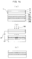
- Fig. 1 represents cross-sectional views of the first electrostatic information recording medium.
- Fig. 1 (a) shows the case where there is no support member, and
- Fig. 1 (b) the case with a support member.
- 110 is an electrostatic information recording medium, 111 an electric charge retaining layer, 113 an electrode layer, 115 a support member, and 120 a protective layer.
- the first electrostatic information recording medium is formed by laminating an electric charge retaining layer 111, consisting of an insulating layer having specific resistance of 1014 - 1018 ⁇ cm on an electrode 113 in order to increase the electric charge retaining property.
- such materials can be used as polyethylene, vinyl chloride resin, polypropylene, styrene resin, ABS resin, polyvinyl alcohol, acryl resin, acrylonitrile-styrene resin, vinylidene chloride resin, AAS (ASA) resin, AES resin, cellulose derivative resin, thermoplastic polyurethane, polyvinyl butyral, poly-4-methylpentene-1, polybutene-1, rosin ester resin, etc.
- ASA ASA
- AES resin cellulose derivative resin
- thermoplastic polyurethane polyvinyl butyral
- poly-4-methylpentene-1 polybutene-1
- rosin ester resin etc.
- fluororesin such materials can be used as polytetrafluoroethylene (PTFE), tetrafluoroethyleneperfluoroalkylvinylether copolymer (PFE), tetrafluoroethylene-hexafluoropropylene copolymer (FEP), tetrafluoroethylene-hexafluoropropylene-perfluoroalkylvinylether copolymer (EPE), tetrafluoroethyleneethylene copolymer (ETFE), polychlorotrifluoroethylene (PCTFE), chlorotrifluoroethylene-ethylene copolymer (ECTFE), etc.
- PTFE polytetrafluoroethylene
- PFE tetrafluoroethyleneperfluoroalkylvinylether copolymer
- FEP tetrafluoroethylene-hexafluoropropylene copolymer
- EPE tetrafluoroethylene-hexafluoropropylene-perflu
- polyparaxylylene given by the following structural formula can be used: (The above Type C is not limited to the substance of the above structure, and it may be such substance that one of the sites other than the main chain bonding sites in the benzene ring is substituted by chlorine; Also, Type D may be the substance with two of the sites substituted by chlorine.)
- the features of the first electrostatic information recording medium lie in the method to form the electric charge retaining layer. Specifically, when insulating material is laminated on an electrode to form the electric charge retaining layer, the electrode is heated by resistance heating (heating by connecting electric current to the electrode layer) to vacuum-deposit the insulating material and to laminate it on the heated electrode layer, or the insulating material is sputtered by argon discharge and is laminated on the heated electrode layer.
- the insulating material may be laminated on the electrode layer by vacuum deposition or by sputtering and is then heated in an oven to produce the electrostatic information recording medium.
- the insulating layer serving as an electric charge retaining layer, must have the thickness of 1000 A (0.1 ⁇ m) or more, and it is preferable that it is 100 ⁇ m thick or less from the viewpoint of flexibility.
- protective film 120 may be laminated on the electric charge retaining layer. Insulating macromolecular meterial is dissolved in solvent and is coated on the electric charge retaining layer by spinner coating method to film thickness of several hundreds to several tens of ⁇ m.
- Fig. 1 (a) shows the case where the insulating material to be laminated has a certain thickness and has a certain strength by itself, and it is laminated on the electrode layer in thin film form.
- Aluminum plate or the like having a certain strength is used as the electrode, and the support member as described later is not required in this case.
- the electrode, on which the insulating layer is laminated may be formed on the support member 115 as shown in Fig. 1 (b), or the support member may be omitted if the insulating layer is in film form, or electrode layer may be laminated on the insulating layer film by vacuum deposition or other method.
- the electrode may be transparent or semi-transparent or may be non-transparent if there is no need to transmit light. Similarly to the insulating layer, it must have heat-resistant property, and there is no restriction on the material as far as specific resistance is 106 ⁇ cm or less. It may be inorganic metal conductive film, inorganic metal oxide conductive film, or organic conductive film such as tertiary ammonium salt. Such electrode is formed by the methods such as vacuum deposition, sputtering, CVD, coating, metalplating, dipping, or electrolytic polymerization. It is necessary to change the film thickness according to the electrical characteristics of the material of the electrode or to the applied voltage during information recording. The film thickness may be 100 - 3000 A, for example.
- the material and the thickness of the support member as far as it has the strength enough to support the electrostatic information recording medium.
- flexible plastic film, paper, or rigid body such as glass, plastic sheet, etc. may be used.
- Light transmission property is required in some cases when electrostatic information is reproduced.
- the electrostatic information recording medium takes the form of flexible film, tape, or disk
- flexible plastic film is used as the support member.
- inorganic materials such as sheet, or glass having rigidity are used.
- the electrostatic information recording medium can take various forms according to the information to be recorded or to the recording method. For example, it takes the form of general film (single frame, or continuous frame) or disk in case it is used for electrostatic camera. In case digital information or analog information is recorded by laser or the like, it takes the form of tape, disk or card.
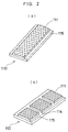
- the electrostatic information recording medium takes the form of flexible film, tape or disk by Fig. 2.
- 111 is an insulating layer, 114 an insulating layer lacking portion, and 115 a support member.
- Fig. 2 (a) shows a type, in which the insulating layer 111 to record is continuous.
- the insulating layer is formed on the entire surface of the support member, consisting of plastic film placed on the electrode layer except both ends of the support member.
- This electrostatic information recording medium is more than two times as long as one screen to be recorded (e.g. at least one frame in case of camera photographing, and track width in case of digital information recording). Naturally, this includes a combination of two or more electrostatic information recording media in longitudinal direction. In this case, there may be a slit zone where insulating layer is lacking between the adjacent insulating layers.
- insulating layer 111 is discontinuous in longitudinal direction.
- Two or more insulating layers are formed in a certain size on the support member.
- the size of the insulating layer depends upon the image and the exposure method of information input unit. For example, it is 35 mm x 35 mm in case of camera photographing, and it is equal to the track width of digital information recording in case of spot input such as laser beam.
- the insulating layer lacking portion formed between the adjacent insulating layers can be used as tracking zone or information input and output. This naturally includes a combination of two or more electrostatic information recording media in longitudinal direction. In this case, there may be a slit zone lacking the insulating layer between the adjacent insulating layer.
- insulating layer 111 is discontinuous in lateral direction.
- the insulating layer is formed discontinuously in lateral direction of the support member, consisting of plastic film placed on the electrode layer, leaving or without leaving both ends of the support member intact.
- Two or more band-like insulating layers are formed on the support member.
- the width of the insulating layer is either equal to or integer multiple of the track width of digital information, and the insulating layer lacking portion formed between adjacent insulating layers is used as tracking zone for information input or output.
- insulating layer is formed on the entire surface of the support member, consisting of circular plastic film placed on the electrode layer, or leaving the insulating layer lacking portion in continuous spiral form.
- circular lacking portion may be formed for driving the input/output unit.
- the insulating layer lacking portion in continuous spiral form can be used as tracking zone for information input and output.
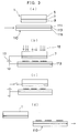
- Fig. 3 is to explain the electrostatic information recording method, in which 1 represents a photosensitive member, 5 a support member, 7 an electrode, 9 a photoconductive layer, 110 an electrostatic information recording medium, 111 an electric charge retaining layer, 113 an electrode, 115 a support member, 17 a power supply, and 18 an information light.
- the photosensitive member is formed by laminating photoconductive layer such as organic photoconductive layer, inorganic photoconductive layer, etc. on the electrode.
- photoconductive layer such as organic photoconductive layer, inorganic photoconductive layer, etc.
- a mixture containing 10 g of poly-N-vinylcarbazole (manufactured by Anan Koryo Co., Ltd.), 10 g of 2,4,7-trinitrofluorenone, 2 g of polyester resin (binder: Byron 200; Manufactured by Toyobo Ltd.) and 90 g of tetrahydrofuran (THF) was prepared at dark place, and this was coated on a glass substrate (1 mm thick), sputtered with In2O3-SnO2 in thickness of about 1000 A, using doctor blade. After this was dried in the air at 60°C for one hour, a photosensitive member having photoconductive layer of about 10 ⁇ m thick was obtained. For more perfect drying, this was further dried naturally for one day.
- the photosensitive member 1 thus prepared was placed face-to-face to the electrostatic information recording medium 110 with a gap of about 10 ⁇ m between them.
- the photoconductive layer 9 irradiated by information light exhibits electrical conductivity, and discharge occurs. Then, the information electric charge corresponding to the information light is accumulated in the electric charge retaining layer.
- the photoconductive layer surface of the photosensitive member is brought into contact with the surface of the electrostatic information recording medium, or they are placed face-to-face without bringing them into contact.
- non-contact condition is maintained mechanically, or they may be placed face-to-face with a spacer between them.
- the spacer may be placed at any point on the surfaces of the photosensitive member and the electrostatic information recording medium.
- the distance between the photosensitive member and the electrostatic information recording medium is 1 - 50 ⁇ m.
- organic material such as plastics or inorganic materials such as glass may be used.
- the recording member is formed by photosensitive member and electrostatic information recording medium instead of photographic film as used in normal camera, and electrostatic latent image is formed on the electric charge retaining layer according to the incident light.
- Mechanical shutter or electrical shutter may be used.
- Light information may be separated into optical components of R, G and B by prism, or color filter may be used to take it out as parallel beams.
- color filter may be used to take it out as parallel beams.
- Color filter can be placed on the support member in the photosensitive member or on the support member having light reflection preventive layer.
- Color filter may be dye type color filter, pigment type color filter, inorganic interference filter type color filter, or holographic color filter recording interference fringes of 3 primary colors. Various arrangements are possible such as stripe type, plane division type, mosaic type. Color filter may be placed separately from the support member or may be placed by laminating on the support member.
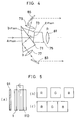
- Fig. 4 shows an optical system for color separation by prism, where 71, 73 and 75 represent prism blocks, 77, 79 and 81 filters, and 83 and 85 reflection mirrors.
- the color separation optical system consists of 3 prism blocks.
- the light information coming from the surface a of the prism block 71 is partially separated and reflected on the surface b. It is further reflected on the surface a, and color light component B is taken out from the filter 77.
- the ramaining light information enters the prism block 73, and advances to the surface c, where it is partially separated and reflected.
- the remaining light components advance straightly further, and color light components G and R are taken out from the filters 79 and 81 respectively.
- the reflection mirrors 83 and 85 By reflecting the color light components G and B by the reflection mirrors 83 and 85, the light components R, G and B can be taken out as parallel beams.
- argon laser 514. 488 nm
- helium-neon laser (633 nm)
- semiconductor laser 780 nm, 810 nm, etc.
- the photosensitive member electrode is set to the same polarity as the polarity of the carrier of photosensitive member.
- laser exposure corresponding to image signal, character signal, code signal or line drawing signal is performed by scanning.
- Analog recording such as image is performed by modulating light intensity of laser, and digital recording such as characters, code and line drawing is performed by ON-OFF control of laser beam.
- the image formed by dots can be formed by ON-OFF control of dot generator on laser beam.
- the spectral characteristics of photoconductive layer in the photosensitive member need not be panchromatic as far as it is sensitive to the wavelength of the laser source.
- electrostatic information is recorded using a photosensitive member
- electrostatic recording using electrode needle head or ion flow head may be performed, or the recording method by optical printer such as laser printer may be adopted.
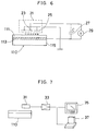
- Fig. 6 shows an example of the potential reading method in the electrostatic information reproducing method.
- 110 is an electrostatic information recording medium
- 21 is a potential reading unit
- 23 is a detection electrode
- 25 is a guard electrode
- 27 is a capacitor
- 29 a voltmeter.
- the potential reading unit 21 is placed face-to-face to the surface of the electric charge retaining layer. Then, the electric field generated by electric charge accumulated inside the electric charge retaining layer gives effect on the detection electrode 23, and induction electric charge equivalent to the electric charge on the electrostatic information recording medium is generated on the detection electrode. Because the capacitor 27 is charged by the electric charge equivalent but having opposite polarity to this induction electric charge, and potential difference corresponding to the accumulated electric charge between electrodes of the capacitor is generated. By reading this value on the voltmeter 29, the potential of the information electric charge can be obtained. By scanning the surface of the electric charge retaining layer by the potential reading unit 21, electrostatic latent image can be outputted as electric signal.
- detection electrode 23 When detection electrode 23 is used alone, resolution is decreased because of the effect of electric field (electric line of force) by electric charge in wider range than the portion facing to the detection electrode of the electrostatic information recording medium.
- a guard electrode 25 grounded around the detection electrode may be disposed. In so doing, the electric line of force is directed toward the direction perpendicular to the plane, and electric line of force acts only on the portion facing to the detection electrode 23.
- the potential at the portion having approximately the same area as the area of detection electrode can be read.
- the accuracy and the resolution of potential reading widely differ according to the shape and size of detection electrode and guard electrode and to the distance from the elctrostatic information recording medium. Therefore, it is necessary to design according to the optimal condition suitable for the desired performance characteristics.
- Laser beam may be irradiated from the direction of the electrode having reflection preventive layer on the image electric charge on the electrostatic information recording medium, and the information may be reproduced through electro-optical crystal, utilizing the modulation by the image electric charge of laser beam.
- the electrostatic information recording medium including support member, electrode, insulating layer, photoconductive layer and protective layer by transparent materials.
- electro-optical crystal it is preferable to place electro-optical crystal in the light path and to use the substance having electro-optical effect such as barium titanate, lithium tantalate (LiTaO3) as the electro-optical crystal.
- Fig. 7 shows approximate arrangement of the electrostatic information reproducing method, where 31 respresents a potential reading unit, 33 an amplifier, 35 a CRT, and 37 a printer.
- electric charge potential is detected by the potential reading unit 31, and the detection output is amplified by the amplifier 33 and is displayed on CRT 35 or is printed out by the printer 37.
- the desired point can be selected and outputted as desired at desired time or the image can be reproduced repeatedly.
- the image can be optically read using the material with its property changing by electric field such as electro-optical crystal. Further, because electrostatic latent image can be obtained as electric signals, it can be used for the recording on the other recording media when necessary.
- Fig. 8 (a) shows the results in case of + charging
- Fig. 8 (b) the results in case of - charging.
- organic photosensitive member 1 and the electrostatic information recording medium as obtained in the Example 1 were placed face-to-face using a polyester film of 10 ⁇ m thick as spacer. Then, DC voltage of 100 V was applied between two electrodes with the photosensitive member as negative, and the medium as positive.
- the surface potential of the medium was measured.
- the surface potential of 100 V was measured by surface potentiometer on the surface of the medium, but the surface potential on unexposed portion was 0 V.
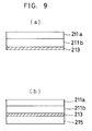
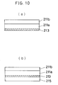
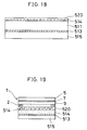
- Fig. 9 and Fig. 10 show cross-sectional views of the second electrostatic information recording medium, where 211 represents an electric charge retaining layer, 211a a resin layer with low glass transition temperature, 211b a heat-resistant insulating layer, 213 an electrode, and 215 a support member.
- the second electrostatic information recording medium has two aspects.
- the first aspect has the structure that heat-resistant resin layer 211b is first laminated on an electrode 213, and resin layer 211a with low glass transition temperature is laminated on it.
- the second aspect has such structure that, as shown in Fig. 9 (a), a resin layer 211a with low glass transition temperature is laminated on an electrode 213 and a heat-resistant insulating layer 211b is further laminated on it as shown in Fig. 10 (a).
- the resin to form the resin layer with low glass transition temperature in this electric charge retaining layer must have the insulating property with specific resistance of 1014 ⁇ ⁇ cm or more at the temperature lower than glass transition temperature.
- the property of resin changes according to the change of molecular chain movement beyond glass transition temperature.
- the insulating property is also decreased at higher than glass transition temperature, and electric charge leaks immediately even when it is accumulated. Accordingly, it is preferable in the normal operating condition to use the resin with glass transition temperature of 20°C or more.
- thermoplastic resins such as polyethylene, ethylene-vinyl acetate copolymer, ehylene-ethyl acrylate and ethylene-methyl acrylate copolymer, polypropylene, polybutylene, methyl pentene resin, polystylene, polyparaxylylene, polyvinyl acetate, polyacrylate, polymetacrylate, vinyl chloride resin, polyvinylidene chloride, fluororesin, polyacrylonitrile, polyvinyl ether, polyvinylketone, polyether, polycarbonate, thermoplastic polyester, polyamide, diene type plastics, polyurethane type plastics, petroleum resin, rosin derivative, terpene type resin, etc., macromolecular resins such as aromatic polyamide, polyphenylene, polyxylylene, polyphenylene oxide, polysulfone, aromatic hetero-ring polymer, etc., silicone resin, inorganic plastics, and further, natural rubber type plastics
- the resin layer resin is dissolved in an adequate solvent, and resin layer is formed by coating, dipping, etc.
- electrostatic information is accumulated on the electrostatic information recording medium, the electrostatic information moves in the resin layer by the effect of electric field and is accumulated. Accordingly, this layer is related to the retaining property of the accumulated electric charge, and the retaining potential of the accumulated electric charge differs according to film thickness.
- the heat-resistant insulating layer is also required to have insulating property with specific resistance of 1014 ⁇ ⁇ cm or more.
- the heat-resistant resin or heat-resistant inorganic substance having glass transition temperature lower than the above resins with low glass transition temperature can be used.
- thermosetting resin such as triazine type resin, polyethylene, ethylene-vinylacetate copolymer, ethylene-ethyl acrylate-ethylene-methyl acrylate copolymer, polypropylene, polybutylene, methylpentene resin, polystyrene, polyparaxylylene, plyvinyl acetate, polyacrylate
- the resin with higher glass transition temperature than the resin layer with low glass transition temperature is used.
- the same material having different glass transition temperature according to the difference in molecular weight can be laminated.
- styrene resin has different molecular weights (Mw) of 348 and 53200 when glass transition temperature is -14°C and 53°C. It is preferable to use the resin with glass transition temperature of 40°C or more.
- the substances such as polytetrafluoroethylene, fluorinated ethylenepropylene, tetrafluoroethylene-perfluoroalkylvinylether copolymer, polyetheretherketone resin, polyparaxylylene given by the following structural formula can be used:
- the above Type C is not limited to the substance of the above structure, and it may be such substance that one of the sites other than the main chain bonding sites in the benzene ring is substituted by chlorine;
- Type D may be the substance with two of the sites substituted by chlorine.
- the resin is dissolved in an adequate solvent, and the layer is formed by coating, dipping, etc.
- Inorganic substances can also be used as heat-resistant insulating layer.
- these are: Inorganic oxides such as SiO2, Al2O3, ZrO2, TiO2, As2O3, B2O3, Bi2O3, CdS, CaO, CeO2, Cr2O3, CoO, GeO2, HfO2, Fe2O3, La2O3, MgO, MnO2, Nd2O3, Nb2O5, PbO, Sb2O3, SeO2, Ta2O5, WO3, V2O5, Y2O5, Y2O3, BaTiO3, Bi2TiO5, CaO-SrO, CaO-Y2O3, Cr-SiO2, LiTaO3, PbTiO3, PbZrO3, ZrO2-Co, ZrO2-SiO2 or inorganic compounds such as AlN, BN, NbN, Si3N4, TaN, TiN, VN, ZrN, SiC, TiC, WC, Al4C3, and silicon dioxide is the most desirable
- photoconductive particles or electrically conductive particles may be given in order to increase the electric charge retaining property.
- photoconductive particle material inorganic photoconductive materials such as amorphous silicon, crystal silicon, amorphous selenium, crystal selenium, cadmium sulfide, zinc oxide, etc. or organic photoconductive materials such as polyvinylcarbazole, phthalocyanine, azo type pigment, etc. are used.
- IA group alkali metal of periodic table
- IB group copper group
- II A group alkali earth metal
- II B group zinc group
- III A group aluminum group
- III B group rare earth group
- IV B group titanium group
- V B group vanadium group
- VI B group chromium group
- VII B group mangaganese group
- VIII group iron group and platinum group
- Carbon, silicon, germanium, tin, and lead can be used as VI A group (carbon group)
- antimony and bismuth can be used as V A group (nitrogen group)
- sulfur, selenium and tellurium can be used in fine powder.
- metal element can also be used in the form of fine powder alloy, organic metal or complex. Further, the above elements can be used in the form of oxide, phosphated compounds, sulfated compounds, or halogenated compounds. Above all, it is preferable to use carbon, gold, copper, aluminum, etc.
- photoconductive or electrically conductive substances are coagulated when evaporated at low pressure of about 10 to 10 ⁇ 3 Torr using vacuum evaporation device on the heated resin layer. They are turned to super-fine particles with diameter of 10 to 0.1 ⁇ m inside the resin layer. The particles may be dispersed into resin solution when coating.
- the heat-resistant insulating layer 211b of Fig. 9 has thickness of 0.1 ⁇ m or more. If it is less than 0.1 ⁇ m, electric charge leaks because the electric charge of the electrode having opposite polarity to the accumulated information electric charge is injected by tunneling phenomenon. There is no restriction to the thickness of resin layer 211a with low glass transition temperature. If thickness exceeds 100 ⁇ m, it is difficult to read the potential when reproducing information electric charge. If high resolution is required in reproducing the information electric charge, it is preferable that resin layer is thin. If it is too thick, electric line of force is disturbed. However, if it is less than 0.1 ⁇ m, the influence by pin hole or the like becomes remarkable, and satisfactory characteristics cannot be obtained.
- heat-resistant insulating layer 211b is laminated with thickness of 0.1 ⁇ m or more. If it is less than 0.1 ⁇ m, the accumulated information electric charge may leak.
- Fig. 9 (b) and Fig. 10 (b) show the cases having support member.
- the support member 215 and the electrode 213 are the same as those used for the first electrostatic information recording method.
- Electrostatic information recording is performed in the same manner as in the information recording on the first electrostatic information recording medium.
- the electrostatic information may be recorded as it is, or information electric charge may be recorded with the electrostatic information recording medium heated to more than the glass transition temperature on the resin with low glass transition temperature and less than the electric charge leaking temperature of the heat-resistant insulating layer.
- the electrostatic information can be more stabilized by heating the electrostatic information recording medium to higher than the glass transition temperature of the resin layer having low glass transition temperature and to lower than the electric charge leaking temperature of the heat-resistant insulating layer.
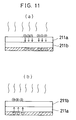
- the mechanism to stabilize the electrostatic information by heating is schematically illustrated in Fig. 11 (a) for the case of the electrostatic information recording medium of Fig. 9, and in Fig. 11 (b) for the case of the electrostatic information recording medium of Fig. 10.
- the reason for the stabilization may be as follows: The electric charge induced by the information electric charge moves apparently by the effect of electric field in the resin layer having low glass transition temperature, which has been turned to electrically conductive by heating. Then, the resin having low glass transition temperature is turned to insulating material due to cooling and it is stably accumulated in the resin layer.
- the electrostatic information recording medium can retain the electrostatic information stably even when it is left without heating. By forcibly heating it, it can reach the stabilized status instantaneously. Compared with the case reaching the stabilization gradually, there is less possibility to cause trouble during the stabilization process. By cooling it after heating, it can be kept at stabilized state. The heating temperature must be lower than the electric charge leaking temperature of the heat-resistant insulating layer.
- the electrostatic information recording medium was left at room temperature and room humidity for 30 days, and the surface potential was measured. As the result, it was maintained at +90 V and -90 V. In the additional test by leaving it for 30 days at 60°C and 20% R.H., the surface potential of ⁇ 80 V was maintained. Further, after leaving it under high humidity condition of 95% R.H. at 40°C for 30 days, the surface potential of ⁇ 70 V was maintained.
- electrostatic information recording medium electric charge was provided by corona charging to have the surface potential of +100 V or -100 V. After heating this in an oven at 45°C for one minute, the surface potential was measured. As the result, the surface potential changed to 80 V and -80 V, and electrostatic information was maintained.
- the electrostatic information recording medium of Fig. 10 was prepared by the same procedure as in the Example 6.
- this electrostatic information recording medium was left for 30 days at room temperature and humidity, and surface potential was measured. It was maintained at +150 V and -120 V.
- surface potential was maintained at +140 V and -110 V.
- surface potential was maintained at +140 V and -100 V.
- this electrostatic information recording medium was left at room temperature and humidity for 30 days, and surface potential was measured. It was maintained at +110 V and -110 V.
- surface potential was maintained at +100 V and -100 V. Further, after leaving it for 30 days under high humidity condition of 95% R.H. at 40°C, surface potential was maintained at +105 V and -105 V.
- the organic photosensitive member used for the electrostatic information recording on the first electrostatic information recording medium, and the electrostatic information recording medium manufactured in the Example 5 were exposed to light under voltage application by the electrostatic information recording method of Fig. 3. After electric charge image of -150 V was obtained with the pattern of line width 20 ⁇ m, it was heated at 40°C for 60 seconds.
- the electrostatic information recording medium having only FEP layer on an electrode was prepared for comparison by the same procedure as in the Example 5, and the same electrostatic information recording was performed.
- Acceleration test was carried out on this electrostatic information recording medium and the comparative medium by leaving them for 30 days under the condition of 40°C and 95% R.H.
- the surface potential was measured and the reproduction by toner development was performed on each of them.
- the surface potential was stabilized at -140 V after heating, and the pattern of 20 ⁇ m could be resolved by toner development.
- the comparison medium surface potential remained at -150 V without attenuating because it was not heated, but the pattern of 20 ⁇ m could not be resolved in the reproduction by toner development.
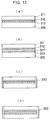
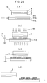
- Figs. 12 (a) and (b) are cross-sectional views of the third electrostatic information recording medium of this invention.
- Figs. 12 (c) and (d) are the cross-sectional views of the information preserving condition after information has been recorded on the electrostatic information recording medium of Figs. 12 (a) and (b).
- 310 is a protective layer, 311 an insulating layer, 311' an insulating layer with thickness of 1000 A or less, 312 a particle layer, 313 an electrode, and 315 a support member.
- the insulating layer must be highly resistant in order to suppress the migration of electric charge, and it is required to have the insulating property with specific resistance of 1014 ⁇ cm.
- the particle layer 312 is formed on electrode by vacuum evaporation, and silica, alumina, etc. are formed on the particle layer by vacuum evaporation, or resin, rubber, etc. are dissolved in solvent and are formed on it by coating or dipping.
- the insulating layer 311' is laminated on the electrode in thickness of 1000 A or less.
- This insulating layer 311' has such function that electric charge is injected into the particles from the electrode 313 by the effect of electric field formed by the image electric charge and that the electric charge is stably maintained in the particles.
- it is preferable that it is laminated in thickness of 1000 A or less, and silica, alumina, etc. are laminated on it by vacuum evaporation, sputtering, etc., or resin, rubber, etc. are dissolved in solvent and are laminated by spinner coating.
- thermoplastic resin or thermosetting resin
- UV-setting resin or energy beam setting resin such as electron beam setting resin, or engineering plastics or rubber
- energy beam setting resin such as electron beam setting resin, or engineering plastics or rubber
- thermoplastic resin it is preferable to use the insulating layer forming materials as described in the first electrostatic information recording medium.
- thermosetting resin unsaturated polyester resin, epoxy resin, phenol resin, urea resin, melamine resin, diallylphthalate resin, silicone resin, etc. can be used.
- radical polymerizing acrylate compound can be used as energy beam setting resin such as UV-setting resin, electron beam setting resin, etc.
- ester compound of acrylic acid or metacrylic acid or their derivatives and having hydroxyl group at both ends There are ester compound of acrylic acid or metacrylic acid or their derivatives and having hydroxyl group at both ends.
- the following compounds can be used: (meta)acrylic ester compound having one polymerizing unsaturated group such as hydroxyethyl acrylate, hydroxypropyl acrylate, hydroxybutyl acrylate, hydroxyethyl metacrylate, hydroxypropyl metacrylate, hydroxybutyl metacrylate, 4-hydroxycyclohexyl acrylate, 5-hydroxycyclooctyl acrylate, 2-hydroxy-3-phenyloxypropyl acrylate, etc.
- glycerol metacrylate or the acrylates given by the following formula can be used: (where R and R' represent methyl group or hydrogen, and R1 represents short chain diole group such as ethyleneglycol, propyleneglycol, diethyleneglycol, butanediole, 1, 6-hexanediole, etc.
- the following compounds can be used: Polycarbonate, polyamide, acetal resin, polyphenylene oxide polybutylene-terephthalate, polyethylene-terephthalate, polyphenylene sulfide, polyimide resin, polysulfone, polyether sulfone, aromatic polyester, polyacrylate, etc.
- the insulating layer to be laminated on the particle layer may be formed by attaching silicon film, polyester film, polyimide film, fluorine-containing film, polyethylene film, polypropylene film, polyparabanic acid film, polycarbonate film, polyamide film, etc. by adhesives.
- the insulating layer to be laminated on the particle layer must be formed with thickness of 1000 A (0.1 ⁇ m) or more from the viewpoint of insulating property, and the thickness is preferably 100 ⁇ m or less from the viewpoint of flexibility.
- the particles to accumulate electric charge are formed by photoconductive material and electrically conductive materials.
- inorganic photoconductive materials such as amorphous silicon, crystalline silicon, amorphous selenium, crystalline selenium, cadmium sulfide, zinc oxide, etc., or organic photoconductive materials such as polyvinylcarbazole, phthalocyanine, azo type pigment, etc. can be used.
- the following materials can be used: The materials of I A group (alkali metal) of periodic table, I B group (copper group), II A group (alkali earth metal), II B group (zinc group), III A group (aluminum group), III B group (rare earth group) IV B group (titanium group), V B group (vanadium group), VI B group (chromium group), VII B group (manganese group), VIII group (iron group and platinum group), or carbon, silicon, germanium, tin, and lead as IV A group (carbon group), antimony, bismuth as V A group (nitrogen group), sulfur, selenium, tellurium as VI A group (oxygen group) are used in fine powder.
- metal element can be used in the form of metallic ion, fine powder alloy, organic metal or complex. Further, the above elements can be used in the form of oxide, phosphated compound, sulfonated compound or halogenated compound. Above all, it is preferable to use carbon, gold, copper, aluminum, etc.
- particle layer of amorphous silicon, amorphous selenium, crystalline selenium, etc. is formed on electrode or on insulating layer by vacuum-depositing the material by low pressure vacuum evaporation device.
- the particle layer forming materials are aggregated when evaporated under low pressure of 10 - 10 ⁇ 3 Torr and are turned to super-fine particles with diameter of 10 - 0.1 ⁇ m.
- the particles are laminated on the surface of electrode or insulating layer, aligned in single layer or in multiple layers.
- the support member and the electrode are the same as those used on the first electrostatic information recording medium.
- Fig. 13 and Fig. 14 are to explain the information recording on the electrostatic information recording medium of Fig. 12 (b).
- Fig. 13 shows the case where the particles are photoconductive particles
- Fig. 14 the case of electrically conductive particles.
- the photosensitive member 1 is placed face-to-face to the electrostatic information recording medium with a gap of about 10 ⁇ m between them as shown in Fig. 13 (a).
- the power source 17 is turned off, and the electrostatic information recording medium is detached from the photosensitive member 1 and total exposure 20 is performed as shown in Fig. 13 (c).
- electric charge is provided evenly, electron and hole carriers are generated on the particle layer of the exposed portion.
- image electric charge generated on the portion, where light enters opposite electric charge is induced on the electrode 313 and moves in the insulating layer 311' by the effect of the electric field.
- electric charge is accumulated in the particle layer in stable condition.
- the electrode In the total exposure, it is necessary to expose the particle layer to generate electron and hole carriers.
- the electrode In case exposure is performed from the direction of insulating layer, the electrode may be non-transparent, while the insulating layer must be transparent or semi-transparent. Thus, it is preferable to use transparent resin.
- transparent electrode such as transparent inorganic conductive layer such as ITO, tin oxide, etc., or vacuum evaporation film of gold or the like must be used.
- particle layer 312 is directly laminated on the electrode 313.
- the information electric charge can be accumulated in the particle layer as described above.
- the electrostatic information recording medium with the information electric charge accumulated in the particles can be coated with the insulating resin on electrode terminals to form the protective layer 310.
- the information electric charge in the particle layer can be permanently maintained.
- the protective layer 310 sealing the electrode terminals is detached to expose the electrode and to read the potential difference from the surface potential, or the terminal is punctured and is brought into contact with the electrode, utilizing the flexibility of the protective layer, and the potential difference between the terminal and the surface potential of electrostatic information recording medium is read.
- the same photosensitive member as the organic photoconductor member used for the electrostatic information recording of the first electrostatic information recording medium was used.
- polyester film of 10 ⁇ m thick as a spacer the electrostatic information recording medium as manufactured in the Example 10 was placed face-to-face to the photoconductive layer surface of the above photosensitive member and was grounded. Then, DC voltage of 700 V was applied between two electrodes with the photosensitive member as positive and the resin layer as negative.
- amorphous silicon photosensitive member it is preferable to apply voltage with photosensitive member as negative, and amorphous selenium photosensitive member as positive.
- silicone resin was coated to seal the exposed portion of the electrode, and the medium was immersed into water. After the immersion, the medium was taken out and water was evaporated. Then, protective film was detached, and potential difference from the medium surface was measured.
- the surface potential of 50 V was measured by surface potentiometer on the surface of the medium, while the surface potential on the non-exposed portion was 0 V.
- surface potential of the electrostatic information recording medium was measured in dark place before total exposure, the surface potential of 100 V was measured on the exposed portion, and this reveals that electric charge is accumulated in selenium particles by total exposure.
- the same exposure was performed by closely attaching a resolution pattern film on the photosensitive member glass substrate during exposure, and then XY-axis scanning was performed on the surface of micro-area surface potential measuring probe of 50 ⁇ 50 ⁇ m on the electrostatic information recording medium.
- the potential data of 50 ⁇ m unit was processed and was enlarged and displayed on CRT by potential-brightness conversion.
- the resolution pattern up to 100 ⁇ m could be confirmed on CRT.
- the electrostatic information recording medium was left for 3 months at room temperature of 25°C and 35% humidity, and the same potential scanning reading was carried out. As the result, the resolution pattern display was exactly the same as that of immediately after the exposure.
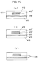
- Figs. 15 (a) and (b) are cross-sectional views of the fourth electrostatic information recording medium
- Fig. 15 (c) is a cross-sectional view to show the aspect at information recording.
- 411 is an insulating layer
- 411' is an insulating layer with thickness of 1000 A or less
- 412 a particle layer 413 a first electrode, 413' a second electrode, 415 a support member and 416 a shorting circuit.
- the fourth electrostatic information recording medium is to record the information on the particle layer 412 as a distribution of electrostatic charge as in the case of the above third electrostatic information recording medium.
- the particle layer may be either photoconductive layer or electrically conductive layer.
- Fig. 15 (a) shows the case where a first electrode 413 is provided on a support member, the insulating layer 411 is laminated in thickness of 1000 A or more, and a second electrode 413' is laminated on the insulating layer with the area smaller than surface of the first electrode. Then, the particle layer 412 is furnished on this second electrode layer, and this second electrode layer and the particle layer 412 are covered by the insulating layer.
- a shorting circuit 416 is formed between the first and the second electrodes as shown in Fig. 5 (c), and information is recorded by the electrostatic information recording method as described above.
- the short-circuit is connected during information recording, and exposure is performed under voltage application. It is released after information recording, and the electrode and the particle layer with the recorded electrostatic information are sealed within the insulating layer.
- the shorting circuit is formed by flexible resin such as rubber on the insulating layer and that it is penetrated by connecting wire to connect with the second electrode and the connecting wire is withdrawn after the information is recorded.
- the connecting wire is penetrated again to connect with the second electrode.
- the particle layer is laminated on the second electrode through the insulating layer 411'.
- This insulating layer 411' is laminated in thickness of 1000 A or less.
- the surface end of the insulating layer laminated on the first electrode is adequately covered and that these layers are laminated by coating or vacuum evaporation.
- the support member and the electrode are the same as those used in the first electrostatic information recording medium.
- Fig. 16 and Fig. 17 are to explain the method to record on this electrostatic information recording medium.
- Fig. 16 shows the case where the particles are photoconductive particles
- Fig. 17 shows the case of electrically conductive particles.
- 416 is a shorting circuit
- 17 a power source
- 18 information light and 20 total exposure.
- the electrostatic information recording medium is placed with a gap of about 10 ⁇ m between them as shown in Fig. 16 (a).
- the shorting circuit 416 in the electrostatic information recording medium is short-circuited as given in Fig. 16 (b).
- electric charge is accumulated on the electrostatic information recording medium.
- the information recording is also performed in the electrostatic information recording medium of Fig. 15 (b), and the information electric charge can be accumulated in the particles in more stabilized condition.
- planar analog recording is performed on the electrostatic information recording medium, the same high resolution as in the silver salt photography can be obtained.
- the electric charge in the particle layer is protected in the insulating layer and it is preserved for long period without being discharged.
- SiO2 insulating layer was vacuum-deposited in thickness of 500 A by sputtering method. Next, this substrate was heated to 100°C on a heater plate, and selenium was vacuum-deposited under low vacuum condition (3 Torr). Thus, selenium particle layer with average diameter of 0.5 ⁇ m was provided in single layer on SiO2 insulating layer.
- this substrate was heated to 100°C on a heater plate, and selenium was vacuum-deposited under low vacuum condition (3 Torr). As the result, selenium layer with average diameter of 5 ⁇ m was furnished on SiO2 insulating layer. Further, the above covering was removed, and 50% xylene solution of silicon resin (TSR-144; Toshiba Silicon Co.) was coated by spinner coating (1000 rpm ⁇ 30 sec.) to cover the selenium particle layer, and the surface was flattened. After drying at 60°C for 3 hours, it was turned to an insulating layer of 10 ⁇ m thick, and the electrostatic information recording medium was prepared.
- TSR-144 Toshiba Silicon Co.
- the same photosensitive member as the organic photoconductor member used for the electrostatic information recording on the first electrostatic information recording medium was used.
- the electrostatic information recording medium prepared in the Example 16 was placed face-to-face to the photoconductive surface of the above photosensitive member and was grounded. Then, the shorting circuit was closed, and the first electrode and the second electrode were connected with each other. DC voltage of 700 V was applied between two electrodes of photosensitive member and the electrostatic information recording medium with the former as positive and the latter as negative.
- amorphous silicon photosensitive member it is preferable that voltage is applied with the photosensitive member as negative and amorphous selenium photosensitive member as positive.
- the same exposure was performed by closely attaching the resolution pattern film on photosensitive member glass substrate during exposure, and the electrostatic information recording medium was then scanned by XY-axis scanning using micro-area surface potential measuring probe of 50 ⁇ 50 ⁇ m.
- the potential data were processed in 50 ⁇ m unit and were enlarged and displayed on CRT by potential-brightness conversion.
- the resolution pattern up to 100 ⁇ m could be confirmed on CRT.
- the electrostatic information recording medium was left for 3 months under the condition of room temperature 25°C and 35%, and the same potential scanning reading was performed. As the result, the resolution pattern was exactly the same as that of immediately after the exposure.
- Fig. 18 is a cross-sectional view of the fifth electrostatic information recording medium.
- Fig. 19 and Fig. 20 are to explain the electrostatic information recording method.
- 511 represents an insulating layer, 513 an electrode, 514 a photoconductive or electrically conductive layer, 515 a support member, and 520 a protective film.
- insulating layer 511 is laminated on the electrode 513, and photoconductive or electrically conductive layer 514 is then laminated.
- the insulating layer forming materials may be the same as those used for the third electrostatic information recording medium.
- Photoconductive layer is a layer where optical carriers (electrons and holes) are generated on the portion irradiated by light and such effect is especially remarkable when electric field is present.
- the materials are inorganic photoconductive materials, organic photoconductive materials, organic-inorganic composite type photoconductive materials, etc.
- the photoconductive materials include inorganic photoconductive materials such as hydrogenated amorphous silicon (a-Si:H), fluorinated amorphous silicon (a-Si:F), amorphous selenium (a-Se), amorphous selenium-tellurium (a-Se-Te), amorphous arsenic-selenium compound (a-As2Se3), amorphous arsenic-selenium compound + Te, cadmium sulfide (CdS), zinc oxide (ZnO), or organic photoconductive materials such as azo pigment, diazo pigment, trisazo pigment, phthalcyanine pigment, perylene pigment, pyrylium dye, cyanine dye, methine dye, etc.
- inorganic photoconductive materials such as hydrogenated amorphous silicon (a-Si:H), fluorinated amorphous silicon (a-Si:F), amorphous selenium (a-Se), amorphous selenium-tell
- hydrozone type there are hydrozone type, pyrazoline type, polyvinylcarbazole type, carbazole type, stilbene type, anthracene type, naphthalene type, tridiphenylmethane type, azine type, amine type, aromatic amine type, etc. including polyvinylcarbazole (PVK), trinitrofluorenone (TNF), PVK-TNF, etc.
- Inorganic materials can be laminated by vacuum evaporation method, sputtering method, CVD method, etc. Coating method may be adopted for zinc oxide.
- Organic materials may be laminated by dissolving in solvent and by coating, or by dipping method, vacuum evaporation method, sputtering method, etc.
- the electrically conductive materials the following materials may be used: The materials of I A group (alkali metal) of periodic table, I B group (copper group), II A group (alkali earth metal), II B group (zinc group), III A group (aluminum group), III B group (rare earth group), IV B group (titanium group), V B group (vanadium group), VI B group (chromium group), VII B group (manganese group), VIII group (iron group and platinum group), or carbon, silicon, germanium, tin, and lead as IV A group (carbon group), antimony and bismuth as V A group (nitrogen group), and sulfur, selenium and tellurium can be used in the form of metallic ion, fine powder alloy, organic metal or complex. Further, the above elements can be used in the form of oxide, phosphonated compound, sulfonated compound, or halogenated compound. Above all, it is preferable to use carbon, gold, copper, aluminum, etc.
- Photoconductive or electrically conductive layer is laminated on the insulating layer in thickness of 0.1 - several ⁇ m.
- photoconductive or electrically conductive layers For the patterning of photoconductive or electrically conductive layers, mask is closely attached on the insulating layer, and photoconductive or electrically conductive material may be laminated by vacuum evaporation method, sputtering method or CVD method. Or, after uniform film is formed on the insulating layer, photoresist is coated, and exposure is performed through mask. Then, patterning is performed by etching. Not only photoconductive or electrically conductive layer, but also the insulating layer may be etched.
- a protective layer 520 is furnished.
- the insulating layer forming materials for example fluororesin, is dissolved in solvent and is coated in thickness of 0.1 - 1 ⁇ m by spinner coating method or by blade coating method.
- the protective layer is overcoated by vacuum evaporation method, sputtering method or CVD method. This protective layer must be thick enough for preventing the damage of the surface or the attenuation of the information electric charge and must be in such thickness that the image electric charge generated on this protective layer can penetrate to the photoconductive layer or electrically conductive layer in each pixel unit.
- the support member and the electrode are the same as those used on the first electrostatic information recording medium.
- the electrostatic information recording medium is placed face-to-face to the photosensitive member 1 with a gap of about 10 ⁇ m. Then, exposure is performed from the direction of photosensitive member. This is the same as the method used for the electrostatic information recording on the first electrostatic information recording medium.
- total exposure is performed after the electrostatic information recording medium is taken out. In so doing, carriers are generated on photoconductive layer.
- the information electric charge moves the protective layer to photoconductive layer, and the information electric charge is accumulated in pattern-like form on the photoconductive layer.
- total exposure is not required, and the information electric charge is accumulated in the patterned conductive layer as described above.
- the information electric charge is accumulated in the patterned photoconductive layer or electrically conductive layer and is sealed by the insulating protective layer.
- the information electric charge can be preserved for long period without being discharged whether it be light or dark.
- a hardening agent (metal catalyst) (trade name: CR-15) was added by 1 wt % (0.2 g) and was mixed well. Then, this was coated on a glass substrate, on which aluminum had been vacuum-deposited in thickness of 1000 A, using doctor blade 4-mil. After drying at 150°C for one hour, a laminated substance of 10 ⁇ m thick was obtained.
- Sibley Microposit 1400 was coated in thickness of 1 ⁇ m on this insulating layer as photoresist, and it was heated at 90°C for 20 minutes. Then, using a mask with line width of 1 ⁇ m, exposure was performed twice in longitudinal and lateral directions, using ultra-high pressure mercury lamp. Then, it was developed and washed, using Sibley Microposit developer, and a-Se was formed in thickness of 0.5 ⁇ m as photoconductive layer by vacuum evaporation method.
- the same photosensitive member as the organic photosensitive member used for the electrostatic information recording on the first electrostatic information recording medium was used.
- This photosensitive member 1 and the electrostatic information recording medium as prepared above were placed with a polyester film 2 of 10 ⁇ m thick as a spacer.
- DC voltage of - 700 V was applied between two electrodes with the photosensitive member as negative and the insulating layer as positive.
- exposure was performed for one second, using halogen lamp of 1000 luxes from the direction of photosensitive member.
- the voltage was turned off.
- the electrostatic information recording medium was taken out. By total exposure, the electrostatic latent image was formed.
- a hardening agent (metal catalyst) (Trade name: CR-15) was added by 1 wt % (0.2 g) and was mixed well. This was coated on a glass substrate, on which aluminum had been vacuum-deposited in thickness of 1000 A, using doctor blade 4-mil. After drying at 150°C for one hour, a laminated substance of 10 ⁇ m thick was obtained.
- a-Se was vacuum-deposited in thickness of 0.1 ⁇ m on this insulating surface as photoconductive layer, and Sibley Microposit 1400 was coated in thickness of 1 ⁇ m by spinner coating method on this photoconductive layer as photoresist.
- protective layer was formed on this photoconductive layer by the same procedure as in the Example 21.
- electrostatic information recording medium Using this electrostatic information recording medium, exposure under voltage application was performed as in the electrostatic image recording method of the Example 21. After the exposure, the power was turned off. The electrostatic information recording medium was taken out, and the potential was read by surface potentiometer. The surface potential of 100 V was detected on the protective film of 0.3 ⁇ m thick. After this electrostatic information recording medium was left for 30 days under the condition of 25°C and 30% humidity, the surface potential was 88 V.
- Fig. 21 and Fig. 22 are to explain this electrostatic information recording medium.
- 603a represents an insulating layer
- 603b a glass
- 603c an orientation layer
- 603d a liquid crystal
- 603e an orientation layer
- 603f an electrode
- 603g a glass
- 605 and 607 are polarizing plates.
- the electrostatic information recording medium was placed face-to-face to the photosensitive member 1 with a gap of about 10 ⁇ m.
- the electrostatic information recording medium consists of a glass plate 603b of 1 mm thick, on which an insulating layer 603a of 10 ⁇ m thick is formed. Liquid crystal 603d is sandwiched by the glass 603b and the glass 603g, on which ITO electrode 603f had been vacuum-deposited in thickness of 1000 A. Inside the glass 603b and the electrode 603f, the orientation layers 603c and 603e are formed. Voltage is applied between the electrodes 7 and 603f from the power source E, and light is irradiated from the direction of the photosensitive member 1, and electric charge is accumulated in pattern-like form on the insulating layer 603a.
- the orientation layers 603C and 603e are placed in such manner that the directions of the orientation intersect with each other at an angle of 90°.
- the molecules of liquid crystal are twisted by 90° between the orientation layers of 603c and 603e.
- polarizing plates 605 and 607 are placed on both sides of the electrostatic information recording medium so that the polarizing directions intersect perpendicularly to each other. Under this condition, the polarizing directions arc not subject to 90° rotation on the portion where molecular arrangement is disturbed by the effect of electric charge. Thus, the polarized light passing through the polarizing plate 607 cannot pass through the polarizing plate 605. On the other hand, the light passes through the polarizing plate 605 on the portion where electric charge pattern is not formed and molecular arrangement is not disturbed because of 90° rotation.
- the color of the polarizing plate 605 can be seen on the portion where electric charge is formed, and the portion where light passes through is seen as bright portion.
- electrostatic pattern can be observed.
- nematic type but also smectic type or cholesteric type liquid crystals can be used.
- polymer dispersed liquid crystal can be used. In the case of polymer dispersed liquid crystal, it is not necessary to use polarizer.
- the image is optically read by irradiating light as shown in Fig. 22, it is desirable to furnish a reflection preventive layer.
- a reflection preventive layer By providing pattern on the electrode 603f, AND computation for electrode pattern and exposed pattern can be performed. Specifically, by visually observing the overlapping of the electrode pattern and the exposure pattern, focus deviation can be detected.
- electro-optical crystal with refractive index varying according to electric field may be used instead of liquid crystal.
- the phase difference of light due to the change in refractive index can be obtained by comparing incident light as reference signal.
- electrostatic pattern can be easily obtained.
- inorganic crystal such as Li Nb2O3 or PLZT but also organic crystal can be used.
- Fig. 23 and Fig. 24 are cross-sectional views of this electrostatic information recording medium.
- 711 is a liquid crystal polymer layer
- 713 an electrode
- 714 an insulating layer
- 715 a support member.
- the seventh electrostatic information recording medium is to record information on a liquid crystal polymer layer.
- thermotropic liquid crystal On the liquid crystal polymer layer 711, thermotropic (heat melting type) liquid crystal is used. When heated, liquid crystal polymer is transferred from solid state to liquid crystal phase and solution phase by phase transition.
- polyester type has very low viscosity in liquid crystal state and exhibits nematic or smectic liquid crystal phase.
- Polyester type substances such as X7G (trade name; Eastman Kodak), Econol (trade name; Sumitomo Chemical Industry), Xydar (trade name; Dartco Japan Petrochemical Industry Co.), Vectra (trade name; Celanese Polyplastics Co.), Novaculate (trade name; Mitsubishi Kasei), Rodrun (trade name; Unitika, Ltd.), Ultrax (trade name; BASF), Idemitsu LCP (trade name; Idemitsu Kosan Co.), Toso LCP (trade name; Toso, Ltd.), or polyester amide type substances, main chain type liquid crystal polymer of polyazo methine type, side chain type liquid crystal polymer with mesogen group having liquid crystal property in skeleton chain such as polymetacrylate, polyacrylate, polysiloxane, polypeptide, polyphosphagen, polyethylimine, etc.
- liquid crystal polymers can be used by mixing two types of more of the above liquid crystal copolymers or low molecular liquid crystal having liquid crystal property may be mixed in polymer.
- liquid crystal polymer By coating liquid crystal polymer on electrode substrate, film with thickness of 1 - several hundreds ⁇ m can be formed.
- liquid crystal polymer can be directly coated on electrode substrate if it has insulating property in solid state. If it has poor insulating property, liquid crystal polymer can be coated on electrode through an insulating layer as shown in Fig. 24.
- the insulating layer 714 the insulating resin in common use as described above is used. The resin must have the heat-resistant property to the temperature higher than liquid crystal range of the liquid crystal polymer and must be able to maintain the information electric charge for a certain period of time within such temperature range.
- fluororesin such as polytetrafluoroethylene, fluorinated ethylene-propylene, tetrafluoroethylene-perfluoroalkylvinylether copolymer, or polyimide resin, polyether-etherketone resin, polyparaxylylene, etc.
- the insulating layer can be formed on electrode by vacuum evaporation method or sputtering method or by coating or dipping after dissolving in solvents. Or, the insulating layer may be formed by attaching the above polymer film by adhesive.
- the film must be thick enough to prevent the penetration of electric charge and is preferably at least 1000 A or more.
- the insulating layer is to prevent the injection of the electric charge discharged from the electrode or from the photosensitive member as described later into the liquid crystal polymer phase. By maintaining the electric charge discharged from photosensitive member, it is possible to keep the orientation on the image exposure portion.
- orientation processing is performed in advance on the surface of the insulating layer by rubbing or using orientation agent. It is desirable to use polyimide film on the insulating layer because heat-resistant property is provided and orientation effect can be increased.
- This polyimide film may be formed by heat treatment after it is coated using polyamic acid. Film-like insulating layer can be laminated by making the orientation directions intersect at right angle.
- the support member 715 is to mechanically support the information recording medium. There is no restriction to its material and thickness as far as it has a certain strength enough to support liquid crystal polymer layer. For example, flexible plastics film, or rigid body such as glass, plastic sheet, etc. are used. It must have light transmitting property and heat-resistant property at the temperature where liquid crystal polymer melts.
- the support member On the other side of the support member, it is desirable to laminate a layer with reflection preventive effect if necessary or to adjust the support member in such thickness to give the reflection preventive effect or further to give reflection preventive sproperty by combining these two.
- the electrode is formed on the support member and must be transparent or semi-transparent. Also, it must have the heat-resistant property as described above, and there is no restriction on the material as far as specific resistance is 106 ⁇ . cm or less.
- Inorganic metal conductive film, inorganic metal oxide conductive film, organic conductive film such as tertiary ammonium salt can be used.
- Such electrode is formed by the methods such as vacuum evaporation, sputtering, CVD, coating, metalplating, dipping, electrolytic polymerization, etc. It is necessary to change the film thickness according to the electrical characteristics of the electrode materials and the applied voltage during information recording. It is 100 - 3000 A, for example, and it is formed on the entire surface between the support member and liquid crystal polymer layer or according to the pattern of liquid crystal polymer layer.
- Fig. 25 is to explain the information recording method.
- the electrostatic information recording medium is placed face-to-face with a gap of about 10 ⁇ m (Fig. 25 (a)).
- liquid crystal polymer layer is exposed to light under voltage application by heating to the liquid crystal temperature range as shown in Fig. 25 (b).
- liquid crystal polymer layer it may be heated by resistance heating in the support member, or only the information recording medium may be heated by external heating means.
- the orientation of liquid crystal polymer molecules is formed on the exposed portion under voltage application.
- the image electric charge is formed by discharging. Because liquid crystal polymer is sensitive to low voltage in some cases, the voltage distribution on liquid crystal polymer layer should be adjusted to fall within the operating voltage range by properly setting the voltage distribution on the photosensitive member, the air gap and the information recording medium.
- Fig. 26 shows an example of the information recording and reproducing method.
- 720 is laser, 721 a 1/4 wavelength plate, 722 an analyzer, and 723 a photodetector.
- the electrode on the information recording medium should be grounded, and it is scanned by laser beam from laser 720 from lower portion of the information recording medium.
- the polarization means consisting of a 1/4 wavelength plate 721 and an analyzer 722 placed in the optical path, the polarized laser beam is detected by the photodetector 23, and the information in the orientation of the liquid crystal polymer layer can be reproduced. Or, it can also be reproduced by natural light.
- an electrode of indium tin oxide (ITO) was laminated in thickness of 1000 A by sputtering method.
- a liquid crystal polymer phase transition temperature °C, g36n108i
- acrylate as main skeleton and mesogen group and containing the repeating unit given by:
- methylethylketone mixed solvent using a blade coater to have the thickness of 10 ⁇ m when dried.
- an electrostatic information recording medium prepared in the Example 24 was placed face-to-face with polyester film of 10 ⁇ m thick as a spacer, and it was grounded. Then, the information recording medium was placed on a heating plate (not shown) heated at 50°C, and DC voltage of 600 V was applied between both electrodes with the photosensitive member as negative and liquid crystal polymer layer as positive. Under voltage application, exposure was performed for 1 second with halogen lamp of 1000 luxes as light source from the side of photosensitive member, and the information was recorded on the liquid crystal polymer layer.
- Figs. 27 (a) and (b) are cross-sectional views of the eighth electrostatic information recording medium.
- 810 is an insulating layer, 811 an electrophoretic substance layer or electrochromy layer, 812 a thermoplastic resin layer, 813 an electrode, and 815 a support member.
- the thermoplastic resin layer 812 is formed of thermoplastic resin material having specific resistance of 1014 - 1018 ⁇ . cm. It is softened at heat development, and the ionized dye and the ionized pigment in the electrophoretic substance layer are diffused in the direction of the electrode by the effect of electric field, which is formed by image electric charge accumulated in the insulating layer 810.
- thermoplastic resin the same substances as the insulating layer forming materials described for the first electrostatic information recording medium can be used.
- thermoplastic resin layer must be the resin having transparent or semi-transparent property.
- the thermoplastic resin layer can be formed by dissolving the above thermoplastic resin in solvent and by coating or dipping or by vacuum evaporation or sputtering methods.
- the thickness of the resin layer is preferably 1 ⁇ m or more. From the viewpoint of flexibility, it is preferably 100 ⁇ m or less.
- cation dye with its counter anion belonging to Lewis acid of halogen such as Cl ⁇ , I ⁇ , etc.
- halogen compounds such as C10 ⁇ , C102 ⁇ , C103 ⁇ , BF4 ⁇ , PF6 ⁇ , etc.
- the substances of diallylmethane type, triallylmethane type, thiazole type, methine type, xanthene type, oxazine type, thiazine type, azine type, acridine type, or azo type having the entire molecule as cation or anion can be used.
- metal complex salt dyes such as core metal, chromium, cobalt, etc.
- core metal chromium, cobalt, etc.
- ionic pigment can be used.
- soluble azo type pigment for example, with water-soluble base laked to metal and turned to insoluble can be used, or organic pigment forming metal complex such as phthalocyanine type pigment can be used.
- electrophoretic substance layers can be formed by dissolving the following substances in binder or dispersed in binder and by coating it on the above thermoplastic resin layer: Thermoplastic resin, silicone resin, styrene-butadiene copolymer resin, epoxy resin, acryl resin, unsaturated or saturated polyester resin, polycarbonate resin, polyvinyl alcohol resin, phenol resin, polymethyl-metacrylate resin, melamine resin, polyimide resin, etc. Or, only the electrophoretic substance may be formed on the thermoplastic resin layer by sputtering, vacuum evaporation, etc. The thickness is preferably about0.1 - 10 ⁇ m.
- electrochromy layer 811 may be formed.
- the electrochromy layer is based on the principle that reversible oxidation and reduction reaction can be induced and color can be developed by the effect of electric field generated by the information electric charge in the insulating layer by turning thermoplastic resin layer to electrically conductive at the heat development.
- the electrochromy layer can be laminated on the thermoplastic resin layer by coating, vacuum evaporation, etc.
- the substance to develop color by reduction such as tungsten oxide (WO3), molybdenum oxide (MoO3), vanadium oxide (V2O5), heptylbiologen, polybiologen complex, tetrathiofluvalene, pasophenanthroline complex can be used.
- the substances to develop color by oxidation such as iridium oxide (IrO x ), rhodium oxide (RhO x ), nickel oxide (NiO x ), chromium oxide (CrO x ), prussian blue complex, ruthenium purple complex, indium nitride (InN), polythiophene (polypyrrole), styryls, or the substances to develop color by oxidation and reduction such as rare earth phthalocyanine, anthraquinone-pyrazoline mixture can be used.
- the insulating resin materials with high glass transfer temperature can be used.
- fluororesin, polyether-etherketone resin, polyparaxylylene resin, etc. can be used. It is preferable to laminate by film laminating method, coating method, vacuum evaporation method, etc. in thickness of 0.1 - 10 ⁇ m, or more preferably, 1 - 5 ⁇ m.
- the support member and the electrode are the same as those used in the first electrostatic information recording medium.
- the information electric charge is accumulated on the insulating layer of the electrostatic information recording medium.
- the information electric charge can be accumulated by discharge electrode or by placing it face-to-face to the photosensitive member and by the exposure with voltage applied between two electrodes.
- the electrostatic information recording medium is formed, for example, as follows: On a support member 815 made of glass of 1 mm thick, an aluminum electrode of 1000 A is formed by vacuum evaporation, and thermoplastic resin layer is laminated on this electrode in thickness of about 10 ⁇ m. Further, cationic dye layer of 1 ⁇ m thick and an insulating layer of 1 ⁇ m thick are formed.
- the electrostatic information recording medium is placed face-to-face to the photosensitive member 1 with a gap of about 10 ⁇ m, and voltage is applied from the power source 15 between the electrodes 7 and 813. In this case, voltage is applied with the photosensitive member electrode as positive. Information exposure is performed from the photosensitive member, and power is turned off.
- the electrostatic information recording medium may be detached or may not be detached from the photosensitive member.
- the electrode 813 is heated by resistance heater 817, or thermoplastic resin layer is heated by another means and is softened.
- thermoplastic resin layer is heated by another means and is softened.
- electrophoretic substance is diffused toward the electrode substrate.
- resin is hardened again. The diffused particles stay as they are, and information electric charge is converted to the position information.
- electrophoretic substance layer is formed by cationic dye, while the same applies to the case where the other ionic dye or ionic pigment is used.
- electrochromy layer is used instead of electrophoretic substance layer, the same electrostatic information recording method can be used although the diffusion of electrochromy layer does not occur.
- a solution containing 10 g of rosin ester resin (stebelite ester 10) and 50 g of tetrahydrofuran was coated on a glass substrate on which aluminum had been vacuum-deposited in thickness of 1000 A, by spinner coating (1000 rpm, 90 sec.). It was left at 60°C for one hour to dry up the solvent, and uniform film of 5 ⁇ m thick was obtained.
- fluororesin (Saitop; Asahi Glass Co.) was coated on the ionized dye layer. After drying, insulating layer of 1.5 ⁇ m thick was laminated, and the electrostatic information recording medium was prepared.
- a-Se-Te thin film was vacuum-deposited on ITO glass substrate by resistance heating method under vacuum condition of 10 ⁇ 5 Torr. Film thickness was set to 1 ⁇ m. Further, with the vacuum condition maintained, only Se was vacuum-deposited by resistance heating method on a-Se-Te layer to form a-Se layer of 10 ⁇ m thick. Thus, a photosensitive member was obtained.
- the above electrostatic information recording medium was placed face-to-face to the above selenium type photosensitive member with polyester film of 10 ⁇ m thick as a spacer and was grounded.
- DC voltage of +700 V was applied between two electrodes with the photosensitive member as positive and the resin layer as negative.
- an ionized pigment Watchung Red as given by the following formula: was used, and the electrostatic information recording medium was prepared by the same procedure as in the Example 26.
- Thermoplastic resin layer was coated on electrode substrate in the same manner as in the Example 26, and tungsten oxide was laminated in thickness of 1 ⁇ m by EB vacuum evaporation method. Then, fluororesin (Saitop; Asahi Glass Co.) was coated in thickness of 1.5 ⁇ m, and electrostic information recording medium was prepared.
- Fig. 29 is a cross-sectional view of the electrostatic information recording medium, and Fig. 30 is to explain the recording method.
- 911 refers to an insulating layer having electric charge transporting property
- 912 is a non-destructive electric charge injection preventive layer
- 913 an electrode
- 914 an electrically conductive portion
- 915 a support member and 916 a heating unit.
- the insulating layer 911 having electric charge transporting property functions as an insulating layer when voltage is not applied. When voltage is applied (or when image electric charge is generated) and electric charge enters from electrode, such electric charge can be easily moved. In this invention, it is necessary to provide hole transporting property or electron transporting property according to the polarity of the electric charge during reproduction.
- amorphous selenium or organic photosensitive materials having good hole transporting property can be used.
- hydrazone type, pyrazoline type, PVK type, carbazole type, oxazole type, triazole type, aromatic amine type, amine type, triphenylmethane type, polycyclic aromatic compounds, etc. can be used.
- the layer of a-Se can be formed by vacuum evaporation, sputtering method, etc.
- Amorphous selenium, amorphous tellurium, amorphous arsenic selenium compound (a-As2Se3), amorphous arsenic selenium compound (a-As2Se3) + tellurium, etc. may be laminated in single layer or in multiple layers, or various types of amorphous selenium may be combined and laminated.
- organic photosensitive material it is coated by spinner coating method after dissolving in solvent.
- zinc oxide, cadmium sulfide, etc. having good electron transporting property can be used.
- Coating method or CVD method chemical vapor deposition
- zinc sulfide granulates particle size 1 - 100 ⁇ m
- solvent or organic metal such as diethyl zinc or dimethyl zinc
- oxygen gas under low vacuum condition (10 ⁇ 2 - 1 Torr)
- chemical reaction is induced on a substrate heated to 150°C - 400°C to deposit as zinc oxide film.
- silicone resin styrene-butadiene copolymer resin, epoxy resin, acryl resin, saturated or unsaturated polyester resin, polycarbonate resin, polyvinyl acetal resin, phenol resin, polymethyl-metacrylate (PMMA) resin, melamine resin, polyimide resin, etc.
- the thickness is preferably 10 - 50 ⁇ m.
- the type of the electrode and the combination of the insulating layer having electric charge transport property are important, and the present inventor has found that the injection property of electric charge differs according to the type of electrode. For example, when polyvinylcarbazole is used as insulating layer material, electric charge is not injected very much into aluminum electrode, while it is easily injected into electrode if ITO electrode is used. In the present invention, it is necessary to select the combination for easier injection of electric charge when voltage is applied.
- the electrode it is better to select the material for easier injection of electric charge into the insulating layer having electric charge transport property.
- organic photoconductive material such as polyvinylcarbazole
- inorganic metal oxide e.g. indium-tin oxide (ITO) may be used as the electrode.
- non-destructible electric charge injection preventive layer 912 is furnished between the electrode 913 and the insulating layer 911 having electric charge transport property.
- the destructible electric charge injection preventive layer is furnished to prevent the moving of electric charge from the electrode to the insulating layer with electric charge transport property when voltage is applied.
- This electric charge injection preventive layer is divided into two types: Insulating layer having such thickness that electric charge is not moved and the layer, which utilizes rectifying effect.
- the layer has such function that the insulating layer and the electrode are made electrically continuous on this portion by the information writing means such as laser irradiation, or heating by thermal head.
- inorganic insulating materials and organic insulating materials can be used as the materials for this electric charge injection preventive layer.
- TeO x is formed into the thickness of 0.1 - 10 ⁇ m by glow discharge, vacuum evaporation, sputtering, etc. When heated and molten by laser irradiation, these compounds with low melting point can be turned to electrically conductive according to the degree of crystallization, and continuous conductivity can be obtained according to the degree of laser irradiation.
- the following materials are formed in thickness of 0.01 - 1 ⁇ m by glow discharge, vacuum evaporation, sputtering, CVD method, etc.: As2O3, B2O3, Bi2O3, CdS, CaO, CeO2, Cr2O3, CoO, GeO2, HfO2, Fe2O3, La2O3, MgO, MnO2, Nd2O3, Nb2O5, PbO, Sb2O3, SiO2, SeO2, Ta2O5, TiO2, WO3, V2O5, Y2O5, Y2O3, ZrO2, BaTiO3, Al2O3, Bi2TiO5, CaO-SrO, CaO-Y2O3, Cr-SiO, LiTaO3, PbTiO3, PbZrO3, ZrO2-Co, ZrO2-SiO2, AlN, BN, NbN, Si3N4, TaN, TiN, VN, ZrN, SiC, TiC, etc.
- the organic insulating materials there are polypropylene, polyethylene, vinyl chloride, vinylidene chloride, polyester, polyamide, degenerated PVA, acrylpolycarbonate, and silicon resin.
- the film-like materials there are heat-shrinking type film such as polystyrene, polybutadiene, PET, polypropyrene, polyethylene, vinyl chloride, polyamide, degenerated PVA, acryl, straight-chain low molecular weight polyethylene film, etc.
- the material is coated by spinner coating together with solvent. In case of the film-like material, it is coated on electrode by adhesive or sticking agents. When heated by thermal head, the heated portion is shrinked and makes the insulating layer with electric charge transport property electrically continuous with the electrode.
- This layer must have the thickness of 1000 A or more to prevent the injection of electric charge.
- the electric charge transport layer with electric charge transport property having polarity opposite to the polarity of the electrode substrate may be furnished by utilizing rectifying effect. Similarly to the above insulating material, the material to cause electric continuity by heating can be used.
- This electric charge injection preventive layer is formed from inorganic insulating layer, organic insulating layer or organic-inorganic composite insulating layer, and the film thickness is about 0.1 - 10 ⁇ m.
- the electrode is negative, amorphous silicon insulating layer doped with B, Al, Ga, In, etc., amorphous selenium, or organic insulating layer formed by dispersing the following substances can be used: oxadiazole, pyrazoline, polyvinylcarbazole, stilbene, anthracene, naphthalene, tridiphenylmethane, triphenyl-methane, azine, amine, aromatic amine, etc.
- amorphous silicon insulating layer doped with P, N, As, Sb, Bi, etc., ZnO insulating layer, etc. are formed by glow discharge, vacuum evaporation, sputtering, CVD, coating, etc.
- the electric charge injection preventive layer is made of organic material, if a layer to generate heat by light absorption from LED, laser beam, etc. is furnished, optical writing can be performed by such light source. For example, by dissolving dye, pigment, etc. in solvent and by dispersing them, and further, by coating it with binder when necessary, the above electric charge injection preventive layer can be easily destroyed.
- dye or pigment there are direct dye, acidic dye, basic dye, metal complex salt dye, butt dye, sulfide dye, naphthol dye, dispersion dye, reaction dye, fluorescent whitening dye, oxide dye, etc. or pigments such as inorganic pigment, phthalocyanine type organic pigment, dyeing pigment, soluble azo type pigment, insoluble azo type pigment, polyazo type pigment, butt type pigment, fluorescent pigment, etc.
- the support member 915 mechanically supports the insulating layer with electric charge transport property, while it is not required in case the insulating layer 911 is of film-like type. In this case, the above electrode can be formed on one side of film through electric charge injection preventive layer.
- 911 is an insulating layer having light carrier generating property and carrier transport property, and 17 a power source.
- the above electrostatic information recording medium is placed face-to-face to the photosensitive member 1 with a gap of about 10 ⁇ m, and the image electric charge is accumulated on the electrostatic information recording medium by general method as described above.
- the medium is taken out, and total exposure is performed with the wavelength corresponding to the electrostatic information recording medium. Then, light carrier is generated on the portion where image electric charge is present. Light carrier having the same polarity as the image electric charge is pulled toward the electrode of the electrostatic information recording medium and it is moved to the interface of the electric charge injection preventive layer.
- high voltage is applied between the electrode during information recording, high electric field is generated between the image electric charge and the electric charge on the electrode. (If surface potential is 1000 V, electric field strength is 107 V/cm.)
- the material to form the electric charge injection preventive layer has preferably such thickness that the electric charge does not move (1000 A or more).
- the information can be recorded by the method other than the exposure under voltage application as described above.
- Fig. 31 (a) shows the conditions where the electric charge injection preventive layer is cracked or destroyed by shrinking
- Fig. 31 (b) represents the condition where the electric charge injection preventive layer is destroyed when it is turned to electrically conductive by crystallization effect.
- 914a is the portion lacking the electric charge injection preventive layer
- 914b a portion where the electric charge injection preventive layer is crystallized
- 916 a heating means is the portion lacking the electric charge injection preventive layer
- 916 a heating means is the portion lacking the electric charge injection preventive layer.
- the information is thermally inputted to the electric charge injection preventive layer by heating means 916 such as thermal head, laser beam, etc. from upper or lower portion of the electrostatic information recording medium.
- the electric charge injection preventive layer is shrinked or cracked to make the insulating layer with electric charge transport property electrically continuous with the insulating layer.
- the electrically continuous portion corresponding to the information can be formed, and the information can be recorded in the form of (0.1) signals.
- Fig. 31 (b) shows the case where the electric charge injection preventive layer is formed using low melting compound such as tellurium oxide.
- the electric charge injection preventive layer is molten on that portion and is crystallized when cooled down.
- Analog recording of the information is performed according to the principle that it is turned to electrically conductive due to the degree of crystallization.
- optical recording by laser can be performed.
- As light source argon laser (514. 488 nm), helium-neon laser (633 nm), or semiconductor laser (780 nm, 810 nm, etc.) can be used.
- Laser exposure corresponding to image signal, character signal, code signal, line drawing signal is performed by scanning from above or below of the electrostatic information recording medium.
- the analog recording such as image recording is performed by modulating the luminous intensity of laser, while digital recording such as character, code, line drawing, etc. is performed by ON-OFF control of laser beam.
- image is formed by dots, it is formed by dot generator ON-OFF control of laser beam.
- Fig. 32 shows cross-sectional views of the electrostatic information recording medium where the information is recorded.
- Fig. 32 (a) total charging is performed on upper surface of the insulating layer of the electrostatic information recording medium as shown in Fig. 32 (a) by corona charge or by applying voltage from the opposing electrodes.
- the electrode and the electric charge transport layer are electrically continuous on the portion, which lacks the electric charge injection preventive layer, and electric charge moves from the electrode.
- the electric charge on the insulating layer with electric charge transport property is neutralized, and electric charge remains on the portion without patterning.
- This electric charge is developed by toner and can be used for electrostatic printing. Or, the information in positive state can be reproduced.
- SiO2 was formed in thickness of 0.2 ⁇ m as electric charge injection preventive layer by the sputtering method.
- mixture solution containing 10 g of poly-N-vinylcarbazole (Anan Koryo Co., Ltd.), 10 g of 2,4,7-trinitrofluorenone, 2 g of polyester resin (binder; Byron 200; Toyobo), and 90 g of tetrahydrofuran (THF) prepared in dark place was coated using doctor blade. After drying at 60°C for one hour in the air, the electrostatic information recording medium having the insulating layer with electric charge transport property of about 10 ⁇ m thick was obtained.
- biaxial stretching ethylene film was laminated on the electrode using adhesive.
- mixture solution containing 10 g of poly-N-vinylcarbazole (Anan Koryo Co., Ltd.), 10 g of 2,4,7-trinitrofluorenone, 2 g of polyester resin (binder; Byron 200; Toyobo), and 90 g of tetrahydrofuran, prepared in dark place was coated by doctor blade. After drying at 60°C for about one hour in the air, the electrostatic information recording medium having insulating layer with electric charge transport property of about 10 ⁇ m thick was obtained.
- tellurium oxide was formed as the electric charge injection preventive layer by sputtering Te under oxygen atmosphere in thickness of 1 ⁇ m.
- the pattern scanning exposure was performed by He - Ne laser (633 nm) of 15 mW, spot diameter of 5 ⁇ m ⁇ and 10 ms from the upper surface of the electrostatic information recording medium as prepared in the Example 29.
- corona charge was performed on the surface of the electrostatic informatin recording medium with - 6 kV.
- surface potential was 0 V on the exposed portion and -450 V on the non-exposed portion.
- Toner could not be attached on the portion, on which He-Ne laser was irradiated, and clear (0.1) printing could be performed.
- Fig. 30 (a) the same photosensitive member as the organic photosensitive member used on the electrostatic information recording on the first electrostatic information recording medium was used.
- This organic photosentsitive member was placed face-to-face to the electrostatic information recording medium as prepared in the Example 31 with a polyester film of 10 ⁇ m thick as a spacer, and DC voltage of -700 V was applied between two electrodes with photosensitive member as negative and the insulating layer electrode as positive. Under voltage application, pattern exposure was performed for one second using halogen lamp of 1000 luxes as light source from the direction of the photosensitive member. Upon completion of the exposure, voltage was turned off.
- the electrostatic information recording medium was taken out, and white light of 10 luxes was irradiated on the entire surface for 10 second. Then, corona charge (-6 kV) was performed in dark place. When surface potential was measured it was 0 V on the pattern exposed portion and -300 V on the non-exposed portion. When reproduced on CRT, pattern image was reproduced.
- the electrostatic pattern on the electrostatic information recording medium is characterized by very high resolution, whereas it is extremely difficult to read this at high accuracy.
- the potential reading method depends much upon scanning density of the reading head, and the reading with high resolution is not achievable.
- Fig. 33 and Fig.34 are to explain the electro-optical reading method of the electrostatic pattern of the present invention.
- 51 is an electrostatic pattern reading unit
- 51a and 51h are reflection preventive layers
- 51b and 51g are glasses
- 51c is a transparent electrode
- 51d and 51f are orientation layers
- 51e liquid crystal 100 an electrostatic information recording medium
- 111 an insulating layer
- 113 an electrode
- 115 a glass support member
- 55 and 57 are polarizing plates.
- the electrostatic information recording medium 100 consists of a transparent glass support member 115, on which a transparent electrode 113 and an insulating layer 111 are laminated, and on the backside of which a reflection preventive layer 120 is formed.
- a transparent glass support member 115 on which a transparent electrode 113 and an insulating layer 111 are laminated, and on the backside of which a reflection preventive layer 120 is formed.
- electric charge is accumulated in pattern-like form by the exposure under voltage application as described above.
- the electrostatic pattern reading unit 51 placed face-to-face to this has such structure that a liquid crystal 51e is sandwiched by orientation layers 51d and 51f and by glasses 51b and 51g and that reflection preventive layers 51a and 51h are provided on the surface of the glasses. Further, a transparent electrode 51c is furnished between the glass 51b and the orientation layer 51d and it is to be short-circuited whth the electrode 113 of the electrostatic information recording medium, on which electrostatic pattern is formed.
- the orientaion layers 51d and 51f are placed in such manner that the directions of the orientations intersect with each other at right angle. Therefore, the molecules of liquid crystal are twisted by 90 degrees between the orientation layers of 51d and 51f.
- a reflection preventive layer 120 is provided on the backside of the electrostatic information recording medium 100, and light is irradiated from the direction of the electrostatic information recording medium so that electro-optical reading can be performed with the electrostatic information recording medium and electro-optical element at the positions close to each other.
- polarizing plates 55 and 57 are placed on both sides of the electrostatic pattern reading unit 51 so that the polarizing directions intersect with each other at right angle. Under this condition, the polarizing direction is not rotated by 90 degrees on the portion where molecular arrangement is disturbed by the effect of electric charge. Thus, the polarized light passing through the polarizing plate 57 cannot pass through the polarizing plate 55. On the other hand, on the portion where electric charge pattern is not formed and molecular arrangement is not disturbed, 90° rotation occurs, and light passes through the polarizing plate 55. Therefore, when viewed from the polarizing plate 55, the portion where electric charge is formed is seen as dark, and the portion where light passes is seen as bright. As the result, the electrostatic pattern can be observed.
- the reading unit when the reading unit is separated from the electrostatic information recording medium and the effect of electric field to liquid crystal is removed, the disturbance of molecular arrangement ceases to be continuous.
- the disturbance When electric field strength is higher than a certain level, the disturbance remains as it is, while it does not remain almost at all at the portion where electric field strength is lower than a certain level.
- the image observed is binary image. Accordingly, to read it as a photograph-like image, it is necessary to place it face-to-face to the electrostatic information recording medium and to read it with the electrodes short-circuited with each other.
- the electrostatic informain recording medium 100 must be transparent and reflection preventive layer 120 must be furnished on its backside.
- the electrode 51c needs not be transparent and it may be aluminum electrode. Also, the reflection preventive layer 51a can be omitted.
- electro-optical effect material in which refractive index changes according to electric field, may be used.
- the phase difference of light due to the change of refractive index can be obtained by comparing the incident light as reference signal.
- electrostatic pattern can be easily obtained.
- the electrostatic pattern with high resolution formed on the electrostatic information recording medium can be converted to the optical change of the electro-optical element. By optically reading this change of optical property, it is possible to read it on molecular level at high accuracy.
- the electrostatic information recording medium per mm2 the information can be accommodated, which corresponds to a color printed matter of A3 size having 175 lines.
- the information density of the electrostatic information recording medium of this invention is 8 ⁇ 108 bit/cm2.
- the electrostatic information recording medium of the present invention can be laminated on card material such as prepaid card, credit card, etc. and can be used as electrostatic information recording card.
- the surface of the electric charge carrying layer is exposed and is embedded in card material, or it is attached and laminated on card material.
- the recording form of the information may be electric charge or toner through toner development.
- the electrode of the electrostatic information recording medium is partially exposed from adequate point to connect it to the photosensitive member electrode. This makes it possible to record the information not only in case the recorded information is turned to the form of a card, but also in case where electrostatic electric charge recording medium with no recorded information is turned to the form of a card and information can be recorded when it is used.
- protective film may be laminated on the electric charge carrying layer or it may be detachable, or the protective film may be thin film so that information can be recorded from above the protective film.
- the recorded electric charge can be preserved as it is or through toner development. Also, it is possible to display on CRT or to print on printer by potential reading means and by reproduction means. Also, it is possible to utilize the reading means, which is used on optical card.
- the information When the information is recorded in electrostatic pattern, it is not visible. Thus, it is possible to use a means to prevent the falsification of cards. Or, the memory capacity is high and information can be recorded on a plane by plane exposure and information can be processed on plane. It is also possible to input or output electric signals or to input the image data on plane, and the types of the data include analog, digital, image, sound and (0.1) information recording. Also, it can be used as external memory of computer. The recorded information can be easily erased.
- the electrostatic information recording medium comprises the information recording area for characters, line drawing, image, code, and (1.0) information and sound information recording area.
- the electrostatic information recording medium of this invention can be used as various types of magnetic card and IC card, optical card of ROM type, DRAW type and EDRAW type optical card or marking card by converting the information input means and using this medium as a master. Also, it is possible to use by replacing the recording areas.
- this medium can be used as ID card, prepaid card, credit card, desktop electronic calculator, electronic notebook, camera, medical record card, timetable, map, electronic lock (key), mini-book, visiting card, sensor, dust remover, battery, bar code, orchestral background music for amateur singers, message (communication means such as postcard), phonograph, game, or learning tools.
- This electrostatic recording card can be used as a recording medium in banking system, ID system, prepaid system, credit system, ticket-issuing system, medical diagnostic system, navigation system, electronic locking system, message system, game system, learning system, etc.
Landscapes
- Physics & Mathematics (AREA)
- General Physics & Mathematics (AREA)
- Optics & Photonics (AREA)
- Photoreceptors In Electrophotography (AREA)
- Printers Or Recording Devices Using Electromagnetic And Radiation Means (AREA)
Applications Claiming Priority (16)
| Application Number | Priority Date | Filing Date | Title |
|---|---|---|---|
| JP6426489 | 1989-03-16 | ||
| JP6426489A JPH02244053A (ja) | 1989-03-16 | 1989-03-16 | 電荷保持媒体の製造方法 |
| JP64264/89 | 1989-03-16 | ||
| JP1066796A JP2597705B2 (ja) | 1989-03-18 | 1989-03-18 | 電気光学材料層を有する電荷保持媒体 |
| JP6724289A JPH02245758A (ja) | 1989-03-18 | 1989-03-18 | 内部蓄積型静電画像記録媒体 |
| JP67248/89 | 1989-03-18 | ||
| JP6679389 | 1989-03-18 | ||
| JP1066793A JP2681384B2 (ja) | 1989-03-18 | 1989-03-18 | 静電パターン情報の電気光学的読み取り方法及び装置 |
| JP6724289 | 1989-03-18 | ||
| JP6724889 | 1989-03-18 | ||
| JP6724889 | 1989-03-18 | ||
| JP66796/89 | 1989-03-18 | ||
| JP6679689 | 1989-03-18 | ||
| JP66793/89 | 1989-03-18 | ||
| JP67242/89 | 1989-03-18 | ||
| PCT/JP1990/000341 WO1990010892A1 (en) | 1989-03-16 | 1990-03-15 | Electrostatic data recording medium and electrostatic data recording/reproducing method |
Publications (3)
| Publication Number | Publication Date |
|---|---|
| EP0592662A4 EP0592662A4 (de) | 1992-08-18 |
| EP0592662A1 true EP0592662A1 (de) | 1994-04-20 |
| EP0592662B1 EP0592662B1 (de) | 2000-02-02 |
Family
ID=27523830
Family Applications (1)
| Application Number | Title | Priority Date | Filing Date |
|---|---|---|---|
| EP90904692A Expired - Lifetime EP0592662B1 (de) | 1989-03-16 | 1990-03-15 | Verfahren zur elektrostatischen Aufzeichnung und Wiedergabe von Informationen |
Country Status (5)
| Country | Link |
|---|---|
| EP (1) | EP0592662B1 (de) |
| CA (1) | CA2028814A1 (de) |
| DE (1) | DE69033448T2 (de) |
| ES (1) | ES2144395T3 (de) |
| WO (1) | WO1990010892A1 (de) |
Families Citing this family (1)
| Publication number | Priority date | Publication date | Assignee | Title |
|---|---|---|---|---|
| CN107782767B (zh) * | 2016-08-26 | 2022-01-07 | 深迪半导体(绍兴)有限公司 | 一种气体传感器加热盘及加工方法 |
Citations (31)
| Publication number | Priority date | Publication date | Assignee | Title |
|---|---|---|---|---|
| GB799829A (en) * | 1954-10-07 | 1958-08-13 | Horizons Inc | Improvements in memory device |
| US3615389A (en) * | 1959-12-28 | 1971-10-26 | Gen Electric | Direct image transfer to thermoplastic tape |
| DE2122755A1 (de) * | 1970-05-08 | 1971-12-02 | Xerox Corp | Abbildungsverfahren |
| US3639640A (en) * | 1969-02-27 | 1972-02-01 | Plastic Coating Corp | Electrostatographic recording element |
| DE1303695B (de) * | 1961-05-31 | 1972-06-29 | Nippon Telegraph And Telephone Public Corp | Elektrographisches aufzeichnungsmaterial |
| US3730710A (en) * | 1969-07-11 | 1973-05-01 | Ricoh Kk | Electrostatic imaging employing a dot electrode |
| DE2011575B2 (de) * | 1969-03-15 | 1975-10-23 | N.V. Philips' Gloeilampenfabrieken, Eindhoven (Niederlande) | Bild wiedergabevorrichtung mit Hilfslichtquelle |
| DE2440485A1 (de) * | 1974-08-23 | 1976-03-04 | Philips Patentverwaltung | Verfahren und aufzeichnungsmedium zur informationsaufzeichnung mit hilfe von laserstrahlen |
| JPS51142333A (en) * | 1975-06-03 | 1976-12-07 | Ricoh Co Ltd | Discharge recording material |
| JPS537240A (en) * | 1976-07-08 | 1978-01-23 | Fujitsu Ltd | Photo-electrostatic recording element |
| US4095280A (en) * | 1975-01-09 | 1978-06-13 | Xerox Corporation | Electrical information storage system using a layer of particulate photosensitive material |
| JPS5388530A (en) * | 1977-01-14 | 1978-08-04 | Mitsubishi Electric Corp | Information recording medium |
| JPS5459161A (en) * | 1977-10-19 | 1979-05-12 | Citizen Watch Co Ltd | Optical device |
| JPS54147042A (en) * | 1978-05-10 | 1979-11-16 | Fuji Photo Film Co Ltd | Image forming material |
| JPS568293A (en) * | 1979-07-03 | 1981-01-28 | Fuji Photo Film Co Ltd | Recording material |
| JPS57140079A (en) * | 1981-02-25 | 1982-08-30 | Olympus Optical Co Ltd | Image pickup device |
| JPS58136036A (ja) * | 1982-02-08 | 1983-08-12 | Tomoegawa Paper Co Ltd | 静電記録体 |
| JPS599666A (ja) * | 1982-07-08 | 1984-01-19 | Konishiroku Photo Ind Co Ltd | 静電記録体 |
| SU1076740A1 (ru) * | 1982-11-19 | 1984-02-29 | Всесоюзный заочный машиностроительный институт | Устройство автоматической фокусировки луча |
| JPS5957261A (ja) * | 1982-09-27 | 1984-04-02 | Canon Inc | 画像形成装置 |
| JPS59171053A (ja) * | 1983-03-18 | 1984-09-27 | Toshiba Corp | 情報記録媒体 |
| JPS60131543A (ja) * | 1983-12-20 | 1985-07-13 | Toshiba Corp | 記録体 |
| JPS613145A (ja) * | 1984-06-15 | 1986-01-09 | Ricoh Co Ltd | 静電記録体 |
| JPS61248788A (ja) * | 1985-04-26 | 1986-11-06 | Hitachi Ltd | 光記録フイルム |
| GB2179006A (en) * | 1985-08-08 | 1987-02-25 | Minnesota Mining & Mfg | Dielectric coating for recording member |
| US4675699A (en) * | 1985-01-18 | 1987-06-23 | Canon Kabushiki Kaisha | Image-recording apparatus |
| EP0275601A1 (de) * | 1986-12-24 | 1988-07-27 | Koninklijke Philips Electronics N.V. | Projektionseinrichtung und die entsprechende Wiedergabeeinrichtung |
| JPS63184758A (ja) * | 1987-01-28 | 1988-07-30 | Toray Ind Inc | 静電記録フイルム |
| JPH01259266A (ja) * | 1988-04-08 | 1989-10-16 | Hamamatsu Photonics Kk | 電圧測定装置 |
| EP0342967A2 (de) * | 1988-05-17 | 1989-11-23 | Dai Nippon Printing Co., Ltd. | Elektrostatisches Informationsaufzeichnungsmedium und elektrostatische Informationsaufzeichnungs- und -wiedergabemethode |
| EP0348982A2 (de) * | 1988-06-30 | 1990-01-03 | Victor Company Of Japan, Limited | Detektorvorrichtung für die Verteilung der auf einer Oberfläche befindlichen Ladung |
Family Cites Families (3)
| Publication number | Priority date | Publication date | Assignee | Title |
|---|---|---|---|---|
| JPS4839032A (de) * | 1971-09-20 | 1973-06-08 | ||
| JPS52142841U (de) * | 1977-04-22 | 1977-10-29 | ||
| JPH0760272B2 (ja) * | 1984-12-12 | 1995-06-28 | 株式会社東芝 | 光導電部材 |
-
1990
- 1990-03-15 ES ES90904692T patent/ES2144395T3/es not_active Expired - Lifetime
- 1990-03-15 WO PCT/JP1990/000341 patent/WO1990010892A1/ja active IP Right Grant
- 1990-03-15 EP EP90904692A patent/EP0592662B1/de not_active Expired - Lifetime
- 1990-03-15 DE DE69033448T patent/DE69033448T2/de not_active Expired - Fee Related
- 1990-03-15 CA CA002028814A patent/CA2028814A1/en not_active Abandoned
Patent Citations (31)
| Publication number | Priority date | Publication date | Assignee | Title |
|---|---|---|---|---|
| GB799829A (en) * | 1954-10-07 | 1958-08-13 | Horizons Inc | Improvements in memory device |
| US3615389A (en) * | 1959-12-28 | 1971-10-26 | Gen Electric | Direct image transfer to thermoplastic tape |
| DE1303695B (de) * | 1961-05-31 | 1972-06-29 | Nippon Telegraph And Telephone Public Corp | Elektrographisches aufzeichnungsmaterial |
| US3639640A (en) * | 1969-02-27 | 1972-02-01 | Plastic Coating Corp | Electrostatographic recording element |
| DE2011575B2 (de) * | 1969-03-15 | 1975-10-23 | N.V. Philips' Gloeilampenfabrieken, Eindhoven (Niederlande) | Bild wiedergabevorrichtung mit Hilfslichtquelle |
| US3730710A (en) * | 1969-07-11 | 1973-05-01 | Ricoh Kk | Electrostatic imaging employing a dot electrode |
| DE2122755A1 (de) * | 1970-05-08 | 1971-12-02 | Xerox Corp | Abbildungsverfahren |
| DE2440485A1 (de) * | 1974-08-23 | 1976-03-04 | Philips Patentverwaltung | Verfahren und aufzeichnungsmedium zur informationsaufzeichnung mit hilfe von laserstrahlen |
| US4095280A (en) * | 1975-01-09 | 1978-06-13 | Xerox Corporation | Electrical information storage system using a layer of particulate photosensitive material |
| JPS51142333A (en) * | 1975-06-03 | 1976-12-07 | Ricoh Co Ltd | Discharge recording material |
| JPS537240A (en) * | 1976-07-08 | 1978-01-23 | Fujitsu Ltd | Photo-electrostatic recording element |
| JPS5388530A (en) * | 1977-01-14 | 1978-08-04 | Mitsubishi Electric Corp | Information recording medium |
| JPS5459161A (en) * | 1977-10-19 | 1979-05-12 | Citizen Watch Co Ltd | Optical device |
| JPS54147042A (en) * | 1978-05-10 | 1979-11-16 | Fuji Photo Film Co Ltd | Image forming material |
| JPS568293A (en) * | 1979-07-03 | 1981-01-28 | Fuji Photo Film Co Ltd | Recording material |
| JPS57140079A (en) * | 1981-02-25 | 1982-08-30 | Olympus Optical Co Ltd | Image pickup device |
| JPS58136036A (ja) * | 1982-02-08 | 1983-08-12 | Tomoegawa Paper Co Ltd | 静電記録体 |
| JPS599666A (ja) * | 1982-07-08 | 1984-01-19 | Konishiroku Photo Ind Co Ltd | 静電記録体 |
| JPS5957261A (ja) * | 1982-09-27 | 1984-04-02 | Canon Inc | 画像形成装置 |
| SU1076740A1 (ru) * | 1982-11-19 | 1984-02-29 | Всесоюзный заочный машиностроительный институт | Устройство автоматической фокусировки луча |
| JPS59171053A (ja) * | 1983-03-18 | 1984-09-27 | Toshiba Corp | 情報記録媒体 |
| JPS60131543A (ja) * | 1983-12-20 | 1985-07-13 | Toshiba Corp | 記録体 |
| JPS613145A (ja) * | 1984-06-15 | 1986-01-09 | Ricoh Co Ltd | 静電記録体 |
| US4675699A (en) * | 1985-01-18 | 1987-06-23 | Canon Kabushiki Kaisha | Image-recording apparatus |
| JPS61248788A (ja) * | 1985-04-26 | 1986-11-06 | Hitachi Ltd | 光記録フイルム |
| GB2179006A (en) * | 1985-08-08 | 1987-02-25 | Minnesota Mining & Mfg | Dielectric coating for recording member |
| EP0275601A1 (de) * | 1986-12-24 | 1988-07-27 | Koninklijke Philips Electronics N.V. | Projektionseinrichtung und die entsprechende Wiedergabeeinrichtung |
| JPS63184758A (ja) * | 1987-01-28 | 1988-07-30 | Toray Ind Inc | 静電記録フイルム |
| JPH01259266A (ja) * | 1988-04-08 | 1989-10-16 | Hamamatsu Photonics Kk | 電圧測定装置 |
| EP0342967A2 (de) * | 1988-05-17 | 1989-11-23 | Dai Nippon Printing Co., Ltd. | Elektrostatisches Informationsaufzeichnungsmedium und elektrostatische Informationsaufzeichnungs- und -wiedergabemethode |
| EP0348982A2 (de) * | 1988-06-30 | 1990-01-03 | Victor Company Of Japan, Limited | Detektorvorrichtung für die Verteilung der auf einer Oberfläche befindlichen Ladung |
Non-Patent Citations (19)
| Title |
|---|
| DATABASE WPIL, no. 88-253907 (36), Derwent Publications Ltd., London, GB; & JP-A-63 184 758 (TORAY IND., INC.) * |
| DATABASE WPIL, week 8836, accession no. 88-253907 [36], Derwent Publications Ltd, London, GB; & JP-A-63 184 758 (TORAY IND., INC.) 30-07-1988 * |
| JAPANESE PATENTS GAZETTE, week 7704, accession no. 77-06457Y [04], Derwent Publications Ltd, London, GB; & JP-A-51 142 333 (RICOH K.K.) 08-12-1976 * |
| JAPANESE PATENTS GAZETTE, week 7925, accession no. 79-46450B [25], Derwent Publications Ltd, London, GB; & JP-A-54 059 161 (CITIZEN WATCH K.K.) 12-05-1979 * |
| JAPANESE PATENTS GAZETTE, week 8001, accession no. 80-00629C [01], Derwent Publications Ltd, London, GB; & JP-A-54 147 042 (FUJI PHOTO FILM K.K.) 16-11-1979 * |
| PATENT ABSTRACTS OF JAPAN, vol. 10, no. 149 (P-461)[2206], 30th May 1986; & JP-A 61 003 145 (RICOH K.K.) 09-01-1986 * |
| PATENT ABSTRACTS OF JAPAN, vol. 11, no. 98 (M-575), 27th March 1987; & JP-A-61 248 788 (HITACHI LTD) 06-11-1986 * |
| PATENT ABSTRACTS OF JAPAN, vol. 14, no. 011 (P-988), 11th January 1990; & JP-A-1 259 266 (HAMAMATSU PHOTONICS K.K.) 16-10-1989 * |
| PATENT ABSTRACTS OF JAPAN, vol. 2, no. 121 (E-63), 12th October 1978; & JP-A-53 088 530 (MITSUBISHI ELECTRIC CORP.) 04-08-1978 * |
| PATENT ABSTRACTS OF JAPAN, vol. 2, no. 42 (E-23), 20th March 1978; & JP-A-53 007 240 (FUJITSU LTD) 23-01-1978 * |
| PATENT ABSTRACTS OF JAPAN, vol. 5, no. 53 (M-63), 14th April 1981; & JP-A-56 008 293 (FUJI PHOTO FILM CO., LTD) 28-01-1981 * |
| PATENT ABSTRACTS OF JAPAN, vol. 6, no. 238 (E-144), 26th November 1982; & JP-A-57 140 079 (OLYMPUS KOGAKU KOGYO K.K.) 30-08-1982 * |
| PATENT ABSTRACTS OF JAPAN, vol. 7, no. 253 (P-235)[1398], 10th November 1983; & JP-A-58 136 036 (TOMOEGAWA SEISHIJIYO K.K.) 12-08-1983 * |
| PATENT ABSTRACTS OF JAPAN, vol. 8, no. 159 (P-289), 24th July 1984; & JP-A-59 057 261 (CANON K.K.) 02-04-1984 * |
| PATENT ABSTRACTS OF JAPAN, vol. 8, no. 97 (P-272), 8th May 1984; & JP-A-59 009 666 (KONISHIROKU SHASHIN KOGYO K.K.) 19-01-1984 * |
| PATENT ABSTRACTS OF JAPAN, vol. 9, no. 26 (P-332), 5th February 1985; & JP-A-59 171 053 (TOSHIBA K.K.) 27-09-1984 * |
| PATENT ABSTRACTS OF JAPAN, vol. 9, no. 296 (P-407), 22nd November 1985; & JP-A-60 131 543 (TOSHIBA K.K.) 13-07-1985 * |
| See also references of WO9010892A1 * |
| WORLD PATENTS INDEX LATEST, week 8443, accession no. 84-268357 [43], Derwent Publications Ltd, London, GB; & SU-A-1076 740 (MECH. ENG. CORRSP. INS.) 28-02-1984 * |
Also Published As
| Publication number | Publication date |
|---|---|
| DE69033448D1 (de) | 2000-03-09 |
| EP0592662A4 (de) | 1992-08-18 |
| WO1990010892A1 (en) | 1990-09-20 |
| ES2144395T3 (es) | 2000-06-16 |
| DE69033448T2 (de) | 2000-07-06 |
| EP0592662B1 (de) | 2000-02-02 |
| CA2028814A1 (en) | 1990-09-17 |
Similar Documents
| Publication | Publication Date | Title |
|---|---|---|
| US5718996A (en) | Electrostatic information recording medium and electrostatic information recording and reproducing method | |
| US5638103A (en) | Method for recording and reproducing information, apparatus therefor and recording medium | |
| US5424156A (en) | Electrostatic information recording medium and method of recording and reproducing electrostatic information | |
| US5731116A (en) | Electrostatic information recording medium and electrostatic information recording and reproducing method | |
| US5514504A (en) | Information recording medium, and information recording a reproducing method | |
| KR100223698B1 (ko) | 정전정보 기록매체 및 정전정보기록 재생방법 | |
| US5439768A (en) | Electrostatic information recording medium and electrostatic information recording and reproducing method | |
| EP0404575B1 (de) | Aufzeichnungsmedium | |
| EP0592662A1 (de) | Elektrostatisches datenaufzeichnungsmedium und elektrostatisches datenaufzeichnungs-/-wiedergabemedium | |
| KR100223697B1 (ko) | 정보기록 재생 처리방법, 처리장치 및 기록체 | |
| EP0455824B1 (de) | Träger für frostbild sowie methode und gerät zum herstellen und lesen eines frostbildes | |
| CA1072663A (en) | Display device having image sense reversal capability | |
| JP3118224B2 (ja) | 静電画像記録再生方法 | |
| EP0471851B1 (de) | Elektrostatisches informationsaufzeichnungsmedium | |
| JP3303998B2 (ja) | 情報記録方法および装置 | |
| JP2962780B2 (ja) | 感光体及び静電情報記録方法 | |
| JPH01290366A (ja) | 静電画像記録再生方法 | |
| JPH02203353A (ja) | 保護膜を有する電荷保持媒体 | |
| JPH06325416A (ja) | 情報記録装置および情報再生方法 | |
| JPH02275960A (ja) | 電荷保持媒体及び電荷保持方法 | |
| JPH02244156A (ja) | 内部電荷保持媒体 | |
| JPH02245765A (ja) | 情報記録媒体及び情報記録再生方法 | |
| JPH01298860A (ja) | 静電潜像読み取り入力スキャナー | |
| JPH02245759A (ja) | 内部蓄積型静電画像記録媒体 | |
| JPH02245758A (ja) | 内部蓄積型静電画像記録媒体 |
Legal Events
| Date | Code | Title | Description |
|---|---|---|---|
| PUAI | Public reference made under article 153(3) epc to a published international application that has entered the european phase |
Free format text: ORIGINAL CODE: 0009012 |
|
| 17P | Request for examination filed |
Effective date: 19901129 |
|
| AK | Designated contracting states |
Kind code of ref document: A1 Designated state(s): DE ES FR GB NL |
|
| 17Q | First examination report despatched |
Effective date: 19951129 |
|
| GRAG | Despatch of communication of intention to grant |
Free format text: ORIGINAL CODE: EPIDOS AGRA |
|
| GRAG | Despatch of communication of intention to grant |
Free format text: ORIGINAL CODE: EPIDOS AGRA |
|
| GRAH | Despatch of communication of intention to grant a patent |
Free format text: ORIGINAL CODE: EPIDOS IGRA |
|
| GRAH | Despatch of communication of intention to grant a patent |
Free format text: ORIGINAL CODE: EPIDOS IGRA |
|
| GRAA | (expected) grant |
Free format text: ORIGINAL CODE: 0009210 |
|
| AK | Designated contracting states |
Kind code of ref document: B1 Designated state(s): DE ES FR GB NL |
|
| REF | Corresponds to: |
Ref document number: 69033448 Country of ref document: DE Date of ref document: 20000309 |
|
| PG25 | Lapsed in a contracting state [announced via postgrant information from national office to epo] |
Ref country code: ES Free format text: LAPSE BECAUSE OF EXPIRATION OF PROTECTION Effective date: 20000316 |
|
| ET | Fr: translation filed | ||
| REG | Reference to a national code |
Ref country code: ES Ref legal event code: FG2A Ref document number: 2144395 Country of ref document: ES Kind code of ref document: T3 |
|
| PLBE | No opposition filed within time limit |
Free format text: ORIGINAL CODE: 0009261 |
|
| STAA | Information on the status of an ep patent application or granted ep patent |
Free format text: STATUS: NO OPPOSITION FILED WITHIN TIME LIMIT |
|
| 26N | No opposition filed | ||
| REG | Reference to a national code |
Ref country code: ES Ref legal event code: FD2A Effective date: 20011010 |
|
| REG | Reference to a national code |
Ref country code: GB Ref legal event code: IF02 |
|
| PGFP | Annual fee paid to national office [announced via postgrant information from national office to epo] |
Ref country code: GB Payment date: 20040126 Year of fee payment: 15 |
|
| PGFP | Annual fee paid to national office [announced via postgrant information from national office to epo] |
Ref country code: NL Payment date: 20040223 Year of fee payment: 15 Ref country code: FR Payment date: 20040223 Year of fee payment: 15 |
|
| PGFP | Annual fee paid to national office [announced via postgrant information from national office to epo] |
Ref country code: DE Payment date: 20040304 Year of fee payment: 15 |
|
| PG25 | Lapsed in a contracting state [announced via postgrant information from national office to epo] |
Ref country code: GB Free format text: LAPSE BECAUSE OF NON-PAYMENT OF DUE FEES Effective date: 20050315 |
|
| PG25 | Lapsed in a contracting state [announced via postgrant information from national office to epo] |
Ref country code: NL Free format text: LAPSE BECAUSE OF NON-PAYMENT OF DUE FEES Effective date: 20051001 Ref country code: DE Free format text: LAPSE BECAUSE OF NON-PAYMENT OF DUE FEES Effective date: 20051001 |
|
| GBPC | Gb: european patent ceased through non-payment of renewal fee |
Effective date: 20050315 |
|
| PG25 | Lapsed in a contracting state [announced via postgrant information from national office to epo] |
Ref country code: FR Free format text: LAPSE BECAUSE OF NON-PAYMENT OF DUE FEES Effective date: 20051130 |
|
| NLV4 | Nl: lapsed or anulled due to non-payment of the annual fee |
Effective date: 20051001 |
|
| REG | Reference to a national code |
Ref country code: FR Ref legal event code: ST Effective date: 20051130 |