EP0589136A2 - Appareil pour lire et pour enregistrer des images - Google Patents
Appareil pour lire et pour enregistrer des images Download PDFInfo
- Publication number
- EP0589136A2 EP0589136A2 EP93105245A EP93105245A EP0589136A2 EP 0589136 A2 EP0589136 A2 EP 0589136A2 EP 93105245 A EP93105245 A EP 93105245A EP 93105245 A EP93105245 A EP 93105245A EP 0589136 A2 EP0589136 A2 EP 0589136A2
- Authority
- EP
- European Patent Office
- Prior art keywords
- image
- signal
- image signal
- bright
- original
- Prior art date
- Legal status (The legal status is an assumption and is not a legal conclusion. Google has not performed a legal analysis and makes no representation as to the accuracy of the status listed.)
- Withdrawn
Links
Images


Classifications
-
- H—ELECTRICITY
- H04—ELECTRIC COMMUNICATION TECHNIQUE
- H04N—PICTORIAL COMMUNICATION, e.g. TELEVISION
- H04N1/00—Scanning, transmission or reproduction of documents or the like, e.g. facsimile transmission; Details thereof
- H04N1/00681—Detecting the presence, position or size of a sheet or correcting its position before scanning
- H04N1/00684—Object of the detection
- H04N1/00702—Position
- H04N1/00705—Position at a plurality of spaced apart locations, e.g. as a sheet is fed through the apparatus
-
- H—ELECTRICITY
- H04—ELECTRIC COMMUNICATION TECHNIQUE
- H04N—PICTORIAL COMMUNICATION, e.g. TELEVISION
- H04N1/00—Scanning, transmission or reproduction of documents or the like, e.g. facsimile transmission; Details thereof
- H04N1/00681—Detecting the presence, position or size of a sheet or correcting its position before scanning
- H04N1/00684—Object of the detection
- H04N1/00718—Skew
-
- H—ELECTRICITY
- H04—ELECTRIC COMMUNICATION TECHNIQUE
- H04N—PICTORIAL COMMUNICATION, e.g. TELEVISION
- H04N1/00—Scanning, transmission or reproduction of documents or the like, e.g. facsimile transmission; Details thereof
- H04N1/00681—Detecting the presence, position or size of a sheet or correcting its position before scanning
- H04N1/00742—Detection methods
- H04N1/00745—Detecting the leading or trailing ends of a moving sheet
-
- H—ELECTRICITY
- H04—ELECTRIC COMMUNICATION TECHNIQUE
- H04N—PICTORIAL COMMUNICATION, e.g. TELEVISION
- H04N1/00—Scanning, transmission or reproduction of documents or the like, e.g. facsimile transmission; Details thereof
- H04N1/00681—Detecting the presence, position or size of a sheet or correcting its position before scanning
- H04N1/00763—Action taken as a result of detection
- H04N1/00769—Comparing, e.g. with threshold
-
- H—ELECTRICITY
- H04—ELECTRIC COMMUNICATION TECHNIQUE
- H04N—PICTORIAL COMMUNICATION, e.g. TELEVISION
- H04N1/00—Scanning, transmission or reproduction of documents or the like, e.g. facsimile transmission; Details thereof
- H04N1/38—Circuits or arrangements for blanking or otherwise eliminating unwanted parts of pictures
Definitions
- the present invention relates to an image reading device for reading an image on an original sheet, and an image forming device for forming an image based on digital image data read by the reading device, more specifically, a digital copying machine which blanks the background other than the original sheet by electrically judging the size of the original sheet from the data read out.
- a white reflection plate on the original sheet cover so as to avoid blackening of the section other than the original sheet when an original sheet having a size smaller than the set sheet size is copied.
- the sheet is placed on the original sheet glass, and the front surface of the sheet glass is covered by the white reflection plate.
- the reflection plate cannot be set on properly on the original, rendering the background section of the original on a copying sheet gray or black.
- Some conventional copying machines include a frame erasing function for the purpose of overcoming such a drawback.
- the frame erasing function detects the size of a sheet used for copy, and controls not to form any image in the sheet's periphery section of a certain width.
- the conventional frame erasing function has a member for erasing images of the unnecessary section in advance by exposing the section to light from its light source before developing the static latent image.
- the position and the size of an original is detected before start of a copying machine, and only the detected region of the original is copied. More specifically, there is a known method in which a metal reflection plate is used for the original sheet press surface of the sheet cover, and pre-scanning is performed with a light beam so as to detect the four corners of the original based on the difference between the intensity of the reflection light from the original and that from the original press surface.
- the frame erasing function using a light source is effective in the case where an original image is copied on a copy sheet at substantially the same magnification; however in the case where the original image is small, the periphery of the original sheet is inevitably blackened.
- detection of the size is in many cases based on typical sizes such as A4 and B4. Further, when the original is placed inappropriately, it is judged to be a wrong size.
- the automatic sheet size detection function cannot detect any sheets but rectangular types. Further, with the copying machines having an original press coated with fluorescent paint, the sheet size cannot be detected when the original press is not appropriately set on the original sheet.
- the purpose of the invention is to provide an image reading device for reading an image, which can accurately detect or erase the region other than the original, regardless of the original size, or how the original is placed, and an image forming device for forming an image, which includes the reading device.
- an image scanning apparatus comprising: means for scanning target areas from a first edge area to a second edge area, the target area including original document areas; means for producing image signal representative of the shade of darkness of areas scanned by the scanning means, the image signals having dark image signals corresponding to the darkness of the target areas except the original document areas and bright image signals corresponding to the darkness of the target areas brighter than the target areas corresponding to the dark image area; means for detecting a first bright image signal and a last bright image signal which are the first signal and the last signal in the bright image signals produced by the producing means in the scanning direction; and means for eliminating the image signal from the image signals corresponding to the first edge areas to the first bright image signals and from the last bright image signal to the image signal corresponding the image signal corresponding to the second edge area.
- an image reading device comprising: means for scanning target areas from a first edge area to a second edge area, the target area including original document areas; means for producing image signal representative of the shade of darkness of areas scanned by the scanning means, the image signals having dark image signals corresponding to the darkness of the target areas except the original document areas and bright image signals corresponding to the darkness of the target areas brighter than the target areas corresponding to the dark image area; means for detecting a first bright image signal and a last bright image signal which are the first signal and the last signal in the bright image signals produced by the producing means in the scanning direction; means for eliminating the image signal from the image signals corresponding to the first edge areas to the first bright image signals and from the last bright image signal to the image signal corresponding the image signal corresponding to the second edge area; and means for forming an image on an image forming medium in accordance with the image signal from the eliminating means.
- image data is read, a picture element of the image data is compared with a reference value so as to detect each of edges of an original sheet, and picture element signals having a value smaller than the reference value located outside the edges of the original sheet are replaced with white data, thereby to blank the section other than the image on the original by white.
- An image reading device for reading an image and an image forming device for forming an image in accordance with the read image data, according to an embodiment of the present invention, with reference to accompanying embodiment.
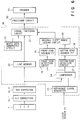
- Fig. 1 is a schematic diagram showing an optical system of an image reading device, for reading an image, the image reading device incorporated in an image forming device
- Fig. 2 is a block diagram showing a processing circuit for an image signal of an image reading device.
- the first and second carriages C1 and C2 are arranged movably in a sub-scanning direction Ss, below an original sheet glass 1.
- the first carriage C1 includes a light source such as a fluorescent lamp La for irradiating light rays or beams on an original sheet 2 via the original sheet glass 1, and the inner surface of the first carriage C1 is made of a recess-shaped mirror.
- a light beam from the fluorescent lamp La irradiates substantially uniformly on a target region such as a band-like region of the original sheet 2, the region being set along the main scanning direction Sm perpendicular to the sub-scanning direction Ss.
- a flat surface mirror 3 so as to transmit the reflection light beam from the original 2.
- the reflection light beam from the original 2 is directed in a direction opposite to the sub-scanning direction by means of the flat surface mirror 3, and reflects on a flat surface mirror 4 provided in the second carriage C2 so as to bend the light beam path at right angle.
- a flat surface mirror 5 which is similar to the mirror 4, for bending the light beam path at right angle.
- a light beam made incident on the flat surface mirror 4 reflects on the flat surface mirror 5 so as to proceed along a light beam path in parallel with a light beam path running from the mirror 3 to mirror 4, in other words, to be direct in the sub-scanning direction.
- a focusing lens 6 by which the light beam proceeding along the main scanning direction and containing the image data of the original 2 is focused toward a CCD sensor 7.
- a filter 8 for transmitting visible rays
- a flat surface mirrors 9 and 10 With this structure, only the visible ray components of the focused light beam concentrated by the focusing lens 6, transmit through the filter 8, and the light beam of the visible components is directed to the flat surface mirrors 9 and 10.
- the light beam reflects on the two flat surface mirrors 9 and 10 each time at right angle, and therefore is directed to a direction opposite to the sub-scanning direction, and then made incident on the CCD sensor 7.
- the first and second carriages C1 and C2 can be moved in the sub-scanning direction Ss as mentioned before, but a motion speed V1 of the first carriage C1 is set to be substantially two times as fast as the motion speed V2 of the second carriage C2. Consequently, even if the reading region of the original 2 in the sub-scanning direction Ss moves due to movement of the first carriage C1, the distance of the light path from the region to the focusing lens 6 is maintained at constant, thereby maintaining the distance to the CCD sensor 7 at constant. Therefore, the magnification of the optical system shown in Fig. 1 is always set at constant regardless of the motion of each of the first and second carriages C1 and C2.
- An original sheet cover 11 as shown in Fig. 3 is provided on the housing of the image forming device such that the cover can be placed on an original sheet glass 1. Further, as shown in Fig. 1, an open/close sensor 32 for detecting opening/closing of the cover 11 is provided for the housing the image forming device.
- a material for absorbing light rays for example, a plate-like light absorbing member 13 made of black sponge, is adhered to an original sheet cover frame 12, and a transparent member 14 such as a transparent vinyl sheet for allowing light rays to transmit therethourgh, and which is brought into tight contact with original sheets, is adhered on the light absorbing member 13.
- reflection of a light beam from the original sheet cover 11 to the optical system shown in Fig. 2 can be suppressed to a low level, and therefore the boundary of the original 2 can be accurately detected.
- the light beam transmitting through the black ink portion of the sheet 2 into the cover 11 can be attenuated sufficiently such as to prevent the light beam from returning to the original 2, thus the image of the original 2 can be sharpened.
- the original sheet cover 11 shown in Fig. 3 the light beam entering into the cover 11 directly or via the original 2 is dispersed by the transparent member 14, and made incident on the light absorbing member 13, where the light is attenuated. Even if there are a slight amount of light components reflecting on the light absorbing material 13, the light components are dispersed once again by the transparent member 14, and therefore the amount of the light components reflecting as shown in Fig. 3? can be reduced to an extremely small level.
- the first and second carriages C1 and C2 start to move in the sub-scanning direction Ss.
- the image on the sheet is transferred in a line-wise fashion one after another along the main scanning direction Sm, and line image signals corresponding to the target images of the document, 2 glass plate 1 and the cover 11 are consecutively output from the CCD sensor 7.
- the image signals represents the shade of darkness of the target areas.
- the line image signals thus output are amplified as serial data in an amplifier 15 shown in Fig. 2, and input to A/D converting and shading correction circuits 16-1 and 16-2, where the analog line image signals are converted to digital line image signals, and shading caused by an irregular irradiation of an exposure lamp La and an irregular sensitivity of the CCD sensor is corrected.
- the shading-corrected digital line image signals are input to a comparison processor 17 and one of input terminals of a selector 18 as the serial data.
- the comparison processor 17 the image signals are compared with the first reference signal Th1 shown in Fig. 4B, and those having a level lower than the first reference signal Th1 are judged to be black. While the image signals having the black level are being input, the selector 18 connects the terminal 18B to which white data is input in accordance with a switching signal from the comparison processor 17, to the output terminal 18C. Consequently, the image signal of black is converted to a white image signal, and output from the output terminal 18C.
- the position P0 of the signal is judged to be a leading edge of the original 2 on the main scanning line corresponding to the image signal, and a switching signal is supplied from the comparison processor 17 to the selector 18 so as to connect the terminal 18A, to which image signals are input, to the output terminal 18C. Therefore, image signals are output from the selector 18 as they are.
- the position PL of the signal is judged to be a tailing edge of the original 2 on the main scanning line corresponding to the image signal, and a switching signal is supplied from the comparison processor 17 to the selector 18 so as to connect the terminal 18B, to which white image data is input, to the output terminal 18C. Therefore, white image signals obtained by converted from a black image are output from the selector 18.
- the level of the first reference signal Th1 is determined based on the level of the dark current of the CCD sensor 7, and the intensity of the reflection light beam from the black ink portion of the original 2. More specifically, in the original sheet cover 11 having a structure shown in Fig. 3, the reflection light beam from the sheet cover 11 has a level lower than the sensitivity of the CCD sensor 7, and therefore the A/D converted value of the level should be theoretically 0. However, in reality, the value will not be 0 due to noise such as a dark current, which is produced in a CCD sensor. Consequently, the level of the first reference signal Th1 is set to be higher than the dark current level. A slight portion of the light beam made incident on black ink portion 2A of the original shown in Fig. 5 reflects on the surface.
- a portion of the light transmits through the black ink portion of the original sheet 2 into the sheet, once again reflecting in the sheet or on the rear surface of the sheet 2.
- the reflection component L1 from the black ink portion 2A of the original sheet 2, the component L2 from the inside of the sheet 2, and the component L3 from the rear surface of the sheet 2 are directed to the CCD sensor 7, where they are detected.
- the level of the first reference signal Th1 is determined such that it is not lower than the level of the image signal thus detected.
- the leading and tailing edge of the original sheet 2 along the main scanning line can be accurately detected by setting the level of the first reference signal Th1 as above.
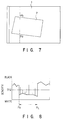
- circuit structure of the device will not be described in more detail with reference to Fig. 6.
- a line memory 20 for consecutively storing digital line image signals each corresponding to one scanning line, is connected to the shading correction circuit 16, to which also connected is a signal switching circuit 21 for selectively and serially outputting either each picture element signal of the digital line image signal for one scanning line or white data picture element signal from the white data generating circuit 22.
- a comparator 24 for comparing a dot signal of the digital line image signal corresponding to one scanning line with the first reference value from the reference value generator 23, is connected to the shading correction circuit 16.
- a cover open/close sensor 32 for detecting opening/closing of the cover.
- the first reference signal Th1 is generated from the reference value generator 23
- the second reference signal Th2 is generated from the reference value generator 23.
- a leading edge detection circuit 25 and a tailing edge detection circuit 27 which generate a leading edge detection signal and a tailing edge detection signal, respectively, by detecting the leading edge and the tailing edge of the original 2 from the comparison result from the comparator 24.
- leading end detection circuit 25 and the tailing end detection circuit 27 respectively connected are a leading end FF (flip-flop) 26 for generating a high-level signal in accordance with the leading edge detection signal, and a tailing edge FF (flip-flop) 28 for generating a high-level signal in accordance with the tailing edge detection signal, and the leading and tailing edge FFs 26 and 28 are further connected to an original sheet range judging circuit 29 for switching the contact point of the signal switching circuit 21 in accordance with the signal outputs.
- leading end FF flip-flop
- a dot signal is supplied to the line memory 20 and the comparator 24 in synchronous with the clock.
- the initial dot signal of one scanning line indicated by the broken line in Fig. 7 is of a black image, and therefore a low-level comparison result is output from the comparator 24.
- the leading and tailing edge FFs 26 and 28 are not set, generating a low-level output in a similar manner to the above. Consequently, the sheet range judging circuit 29 judges that a dot signal out of the sheet range is input, and connects the contact point of the signal switching circuit 21 to the white data generating circuit 22.
- a dot signal corresponding to a black image is supplied from the line memory 20 to the signal switching circuit 21
- a dot signal corresponding to a white image is supplied from the signal switching circuit 21 to the processing circuit 30 in synchronous with the clock.
- the line memory 20 stores the dot signals in the order of input, and the comparator 24 compares each of the dot signals consecutively with the first reference value Th1, and generates high-level dot signals as the comparison results.
- the comparison results are continuously supplied to the leading edge detection circuit 25.
- the leading end detection circuit 25 judges that the dot signal of the leading edge of the original 2 has been input, and supplies a leading edge detection signal to the leading edge FF (flip-flop) 26.
- a high-level signal is output from the leading edge FF 26, and in accordance with the high-level signal from the leading edge FF 26, the original sheet range judging circuit 29 switches the signal switching circuit 21, and outputs the dot signal from the line memory 20 to the processing circuit 30.
- the line memory 20 While the white image corresponding to the region P0-PL on the original 2 is being supplied to the line memory 20 and the comparator 24, the line memory 20 is connected to the processing circuit 30, and the dot signals of the original 2 are directly supplied to the processing circuit 30.
- the line memory 20 stores the dot signals, and the comparator 24 compares each of the dot signals consecutively with the first reference value, and outputs low-level dot signals as comparison results. Then, when a predetermined number of low-level comparison results are supplied to the tailing edge detection circuit 27, the tailing edge detection signal 27 judges that the dot signal of the tailing edge of the original 2 has been input, and supplies the tailing edge detection signal to the tailing edge FF (flip-flop) 28.
- the tailing edge detection signal 27 judges that the dot signal of the tailing edge of the original 2 has been input, and supplies the tailing edge detection signal to the tailing edge FF (flip-flop) 28.
- a high-level signal is generated from the tailing edge FF 28, and in response to the high-level signal from the tailing edge FF 28, the original sheet range judging circuit 29 switches the signal switching circuit 21, and connects the white data generating circuit 23 to the processing circuit. Consequently, even if a dot signal corresponding to a black image is supplied from the line memory 20 to the signal switching circuit 21, a dot signal corresponding to a white image is supplied from the signal switching circuit 21 to the processing circuit 30 in synchronous with the clock.
- the dot signals corresponding to one line are supplied to the processing process 30, the leading and tailing edge FFs 26 and 28 are reset. In other words, the leading and tailing edge FFs 26 and 28 are reset by a scanning signal.
- the line memory 20 serves as a type of buffer. More specifically, until the leading or tailing edge is detected, the dot signal corresponding to the leading or tailing edge is not supplied to the signal switching circuit 21. Consequently, the black dots located outside the original can be converted into white dots.
- printing is executed in accordance with the ink amount signal so as to form an image on an image forming device.
- the section other than the original is printed in white.
- the region other than the original can be converted into a white image, and the region of the image forming medium other than the original can be formed in white.
- the level of the second reference signal Th2 is set to be higher than the level of the first reference signal Th1 as shown in Fig. 8.
- the original sheet cover cannot be closed. Therefore, external light enters in the original sheet glass 1, and the light may be detected by the CCD 7 as of a lower density than that of the black portion of the original 2. This is the reason why the level of the second reference signal Th2 is set to be higher than that of the first reference signal Th1.
- the cover open/close sensor 32 detects that the cover is closed, the second reference signal Th2 is generated from the reference value generator 23 in place of the first reference signal Th1.
- the initial dot signal of one scanning line indicated by the broken line in Fig. 7 is a dot signal corresponding to a black or gray image having a level lower than the second reference signal Th2, and therefore a low-level comparison result is output from the comparator 24.
- the leading and tailing edge FFs 26 and 28 are not set, generating a low-level output in a similar manner to the above.
- the sheet range judging circuit 29 judges that a dot signal out of the sheet range is input, and connects the contact point of the signal switching circuit 21 to the white data generating circuit 22. Hence, a dot signal corresponding to a white image is supplied to the processing circuit 30 in synchronous with the clock.
- the line memory 20 stores the dot signals in the order of input, and the comparator 24 compares each of the dot signals consecutively with the second reference value Th2, and generates high-level dot signals as the comparison results.
- the comparison results are continuously supplied to the leading edge detection circuit 25.
- the leading end detection circuit 25 judges that the dot signal of the leading edge of the original 2 has been input, and supplies a leading edge detection signal to the leading edge FF (flip-flop) 26.
- a high-level signal is output from the leading edge FF 26, and in response to the high-level signal from the leading edge FF 26, the original sheet range judging circuit 29 switches the signal switching circuit 21, and outputs the dot signal from the line memory 20 to the processing circuit 30.
- the line memory 20 While the white image corresponding to the region P0-PL on the original 2 is being supplied to the line memory 20 and the comparator 24, the line memory 20 is connected to the processing circuit 30, and the dot signals of the original 2 are directly supplied to the processing circuit 30.
- the line memory 20 stores the dot signals, and the comparator 24 compares each of the dot signals consecutively with the second reference value Th2, and outputs low-level dot signals as comparison results. Then, when a predetermined number of low-level comparison results are supplied to the tailing edge detection circuit 27, the tailing edge detection signal 27 judges that the dot signal of the tailing edge of the original 2 has been input, and supplies the tailing edge detection signal to the tailing edge FF (flip-flop) 28.
- the tailing edge detection signal 27 judges that the dot signal of the tailing edge of the original 2 has been input, and supplies the tailing edge detection signal to the tailing edge FF (flip-flop) 28.
- a high-level signal is generated from the tailing edge FF 28, and in response to the high-level signal from the tailing edge FF 28, the original sheet range judging circuit 29 switches the signal switching circuit 21, and connects the white data generating circuit 21 to the processing circuit 21. Consequently, a dot signal corresponding to a white image is supplied to the processing circuit 30 in synchronous with the clock.
- the dot signals corresponding to one line are supplied to the processing process 30, the leading and tailing edge FFs 26 and 28 are reset. In other words, the leading and tailing edge FFs 26 and 28 are reset by a scanning signal.
- the first comparator 36 and the switch terminal 36B of the first selector 36 which is switched by the first comparator 34, are connected to the shade correction circuit 16-2, to which an image signal is output.
- a fixed terminal 48C of the second selector 48 To an output fixed terminal of the first selector 36, connected is a fixed terminal 48C of the second selector 48.
- switch terminals 48A and 48B of the second selector 48 connected are input sides of line memories 38 and 39.
- one line serial image data items are input alternately, but when the data items are output, they are read out in the reverse order to that of input by means of a register. More specifically, when one line serial image data items are input to each of the line memories 38 and 39, signal input starts from a digital signal corresponding to the first dot, and signals are input serially in the order, until the digital signal corresponding to the final dot.
- the first and second comparators 34 and 40 are connected to the reference signal generator 23 for generating a reference signal, and to a horizontal synchronous signal generator 44 for generating a horizontal synchronous signal, with which timing for transferring one line serial image data generated by the CCD sensor 7 is obtained.
- the first and second comparators 34 and 40 receives the synchronous from the horizontal synchronous signal generator 44 as a reset signal, and are reset by the synchronous signal.
- the horizontal synchronous signal generator 44 is connected to the F/F 46, and by the output signal from the F/F 46, the third and fourth selectors 48 and 50 are switched over. In other words, the third and fourth selectors 48 and 50 are switched over in response to the horizontal synchronous signal.
- a black dot is replaced with a white dot, and an image signal is corrected in the following manner.
- line image signals are generated consecutively in synchronous with the horizontal synchronous signal from the horizontal synchronous signal generator 44.
- the line image signals generated are amplified as serial data, and input to the A/D converter 16-1, where analog line image signals are converted into digital line image signals.
- the shading of the digital signals caused by an irregular irradiation of an exposure lamp La and an irregular sensitivity of the CCD sensor is corrected by the shading correction circuit 16-2.
- the shading-corrected digital line image signals are input to the first comparator 34 and one of input terminals of the first selector 36 as the serial data.
- a terminal 36B, to which white data is input is usually connected to an output terminal 36C.
- the position P0 of the signal is judged to be a leading edge of the original 2 on the main scanning line corresponding to the image signal, and a switching signal is supplied from the comparator 36 to the selector 36 so as to connect the terminal 36A, to which image signals are input, to the output terminal 36C.
- the terminal 36A is continued to be connected to the terminal 36C until the comparator 36 is reset. Therefore, the converted white dots of the initial group, the following image dots, and one line serial image signal containing black dots of the final group are the second selector 48.
- the fixed contact point 48C is connected to the first switching contact point 48, and therefore the one line serial image signal is input to the first memory from the beginning.
- a horizontal synchronous signal is generated, and transfer of the next (second) one line serial image signal from the CCD sensor 7 is started.
- the comparators 34 and 40 are reset, and the output of the F/F 46 is switched. Consequently, in the selector 36, the fixed contact point 36C is connected to the switching contact point 36A, whereas in the selector 48, the fixed contact point 48C is connected to the switching point 48A. Further, in the selector 50, the fixed contact point 50C is connected to the switching contact point 50B.
- the black dots are replaced with white data as in the case of the first one line serial image signal, and input to the second memory 39 consecutively from the first dot.
- the first one line serial image signal stored in the first memory 38 is read via the third selector 50, starting from the edge dot, and is input to the switching terminal 42A of the fourth selector 42, and the comparator 40.
- a terminal 42B, to which white data is input is usually connected to an output terminal 42C.
- the selector 42 maintains its state in which the terminal 42B to which white data is input is connected to the output terminal 42C. Consequently, the black image signal is converted into a white image signal, and output from the output terminal 42C.
- the position Ph of the signal is judged to be a tailing edge of the original 2 on the main scanning line corresponding to the image signal, and a switching signal is supplied from the comparator 40 to the selector 42 so as to connect the terminal 42A, to which image signals are input, to the output terminal 42C.
- the terminal 42A is continued to be connected to the output terminal 42C until the comparator 40 is reset. Therefore, one line serial image signal is supplied to the processing circuit 30, from the tailing edge dot toward the leading edge dot, in the order of the converted white dots, the following image dots, and the converted white dots. Each time a horizontal synchronous signal is generated, the above-described operation is repeated.
- One-line serial image signals are alternately stored in the memories 38 and 39, and are alternately read out therefrom. Further, black dots are converted into white dots, and are supplied to the processing device 30, starting from the edge dot.
- each dot signal is compared with a reference value, but some dots can be selected as samples to be compared.
- the comparison may be performed for only one of a predetermined number of dot signals, or only a plurality of dot signals.
- the image data of the section where an original sheet is not present can be converted into white data during an image forming operation with a relatively simple structure. Further, detection of whether or not the original is present, and a black/white conversion are performed at real time for each picture element unit, and therefore even if the original is placed obliquely, or has an arbitrary shape, the image data of the section where an original sheet is not present can be converted into white data. Moreover, In the case where it is failed to place an original sheet, or to close the original sheet cover, or the original is three-dimensional and thick, only the original sheet section is read, and copied. Therefore, waste of copy sheets and developer due to erroneous copying can be significantly reduced, and a neat copy with the periphery of a sheet being whitened can be achieved.
Landscapes
- Engineering & Computer Science (AREA)
- Multimedia (AREA)
- Signal Processing (AREA)
- Facsimile Scanning Arrangements (AREA)
- Editing Of Facsimile Originals (AREA)
Applications Claiming Priority (2)
| Application Number | Priority Date | Filing Date | Title |
|---|---|---|---|
| JP280437/92 | 1992-09-25 | ||
| JP28043792A JP3225112B2 (ja) | 1992-09-25 | 1992-09-25 | 原稿読取装置と原稿読取方法 |
Publications (2)
| Publication Number | Publication Date |
|---|---|
| EP0589136A2 true EP0589136A2 (fr) | 1994-03-30 |
| EP0589136A3 EP0589136A3 (en) | 1994-06-15 |
Family
ID=17625043
Family Applications (1)
| Application Number | Title | Priority Date | Filing Date |
|---|---|---|---|
| EP19930105245 Withdrawn EP0589136A3 (en) | 1992-09-25 | 1993-03-30 | Image reading and forming device |
Country Status (3)
| Country | Link |
|---|---|
| US (1) | US5510908A (fr) |
| EP (1) | EP0589136A3 (fr) |
| JP (1) | JP3225112B2 (fr) |
Cited By (6)
| Publication number | Priority date | Publication date | Assignee | Title |
|---|---|---|---|---|
| GB2289182A (en) * | 1994-04-07 | 1995-11-08 | Fujitsu Ltd | Paper end detection apparatus |
| EP0759245A1 (fr) * | 1994-04-04 | 1997-02-26 | Motorola, Inc. | Communication par telecopie avec recepteurs d'appel selectif |
| EP0878957A2 (fr) * | 1997-05-12 | 1998-11-18 | Riso Kagaku Corporation | Appareil de traitement d'image |
| EP0889634A2 (fr) * | 1997-07-04 | 1999-01-07 | SAMSUNG ELECTRONICS Co. Ltd. | Procédé et dispositif de détection de taille d'un document |
| EP0889632A2 (fr) * | 1997-07-02 | 1999-01-07 | Samsung Electronics Co., Ltd. | Procédé pour détecter le bord avant d'un support d'impression |
| EP0889633A2 (fr) * | 1997-07-04 | 1999-01-07 | SAMSUNG ELECTRONICS Co. Ltd. | Procédé et appareil de balayage des documents |
Families Citing this family (19)
| Publication number | Priority date | Publication date | Assignee | Title |
|---|---|---|---|---|
| JP3786213B2 (ja) * | 1993-03-24 | 2006-06-14 | 株式会社東芝 | 画像形成装置 |
| JP3026917B2 (ja) * | 1994-09-30 | 2000-03-27 | キヤノン株式会社 | 原稿自動給送装置及びそれを備えた画像形成装置 |
| US5729024A (en) * | 1995-05-08 | 1998-03-17 | Ricoh Company, Ltd. | Original edge detecting system and optical sensor |
| US5748344A (en) * | 1995-09-25 | 1998-05-05 | Xerox Corporation | System and method for determining a location and orientation in a black and white digital scanner |
| US5917616A (en) * | 1995-09-29 | 1999-06-29 | Canon Kabushiki Kaisha | Image processing apparatus and control method thereof |
| US6271935B1 (en) * | 1998-09-23 | 2001-08-07 | Xerox Corporation | Method to remove edge artifacts from skewed originals |
| US6879730B1 (en) * | 1999-04-12 | 2005-04-12 | Fuji Photo Film Co., Ltd. | Sensitivity correction method and image reading device |
| US6643037B1 (en) * | 1999-09-20 | 2003-11-04 | Hewlett-Packard Development Company, L.P. | Apparatus and method for detecting the presence of a page in an image scanner |
| KR100334114B1 (ko) * | 2000-05-02 | 2002-05-03 | 윤종용 | 스캐너 이미지 정정 방법 |
| US20020105682A1 (en) * | 2001-02-05 | 2002-08-08 | Toshiba Tec Kabushiki Kaisha | Image processing apparatus and image processing method |
| JP3829667B2 (ja) * | 2001-08-21 | 2006-10-04 | コニカミノルタホールディングス株式会社 | 画像処理装置、画像処理方法、画像処理方法実行のためのプログラム及びプログラムを記憶した記憶媒体 |
| JP4997719B2 (ja) * | 2005-06-30 | 2012-08-08 | コニカミノルタビジネステクノロジーズ株式会社 | 画像読取装置、画像読取装置の制御方法、および、画像読取装置を制御するためのプログラム |
| US20090073479A1 (en) * | 2007-09-14 | 2009-03-19 | Kabushiki Kaisha Toshiba | Image scanning apparatus |
| JP4502001B2 (ja) * | 2007-12-20 | 2010-07-14 | コニカミノルタビジネステクノロジーズ株式会社 | 画像処理装置および画像処理方法 |
| JP5531837B2 (ja) * | 2010-02-19 | 2014-06-25 | コニカミノルタ株式会社 | 画像処理装置および画像読取装置 |
| JP5814552B2 (ja) * | 2011-01-31 | 2015-11-17 | キヤノン株式会社 | 画像処理方法及び画像処理装置 |
| US9413912B2 (en) * | 2012-10-26 | 2016-08-09 | Abbyy Development Llc | Scanning device having a bed cover including a pattern of repeated design elements |
| SE538115C2 (sv) | 2014-04-24 | 2016-03-08 | Atlas Copco Rock Drills Ab | Borrigg och borrhuvud till en borrigg |
| JP7401500B2 (ja) * | 2020-10-13 | 2023-12-19 | ティーイー コネクティビティ ジャーマニー ゲゼルシャフト ミット ベシュレンクテル ハフツンク | 電気端子 |
Citations (4)
| Publication number | Priority date | Publication date | Assignee | Title |
|---|---|---|---|---|
| GB2142499A (en) * | 1983-06-07 | 1985-01-16 | Canon Kk | An original image processing apparatus |
| EP0218447A2 (fr) * | 1985-09-30 | 1987-04-15 | Canon Kabushiki Kaisha | Appareil de traitement de signaux d'image |
| WO1989001268A1 (fr) * | 1987-07-24 | 1989-02-09 | Eastman Kodak Company | Appareil et procedes pour localiser les bords et les limites d'un document dans des lignes de balayage video |
| EP0371744A2 (fr) * | 1988-11-29 | 1990-06-06 | Mita Industrial Co. Ltd. | Appareil de traitement d'images |
Family Cites Families (8)
| Publication number | Priority date | Publication date | Assignee | Title |
|---|---|---|---|---|
| US4547810A (en) * | 1982-04-09 | 1985-10-15 | The Associated Press | Portable facsimile transmitter |
| US4763200A (en) * | 1985-04-11 | 1988-08-09 | Minolta Camera Kabushiki Kaisha | Image output apparatus |
| JPH07101913B2 (ja) * | 1986-05-09 | 1995-11-01 | 株式会社東芝 | 画像形成装置 |
| US4899227A (en) * | 1987-01-26 | 1990-02-06 | Canon Kabushiki Kaisha | Image processing apparatus detecting the size or position of an information portion of an original |
| JP3101304B2 (ja) * | 1990-08-02 | 2000-10-23 | キヤノン株式会社 | 画像処理装置 |
| US5253081A (en) * | 1990-12-20 | 1993-10-12 | Fuji Photo Film Co., Ltd. | Image recording device |
| US5157740A (en) * | 1991-02-07 | 1992-10-20 | Unisys Corporation | Method for background suppression in an image data processing system |
| JP3028653B2 (ja) * | 1991-09-13 | 2000-04-04 | 富士ゼロックス株式会社 | 画像処理装置の枠消し方式 |
-
1992
- 1992-09-25 JP JP28043792A patent/JP3225112B2/ja not_active Expired - Fee Related
-
1993
- 1993-03-30 EP EP19930105245 patent/EP0589136A3/en not_active Withdrawn
-
1995
- 1995-03-13 US US08/403,128 patent/US5510908A/en not_active Expired - Fee Related
Patent Citations (4)
| Publication number | Priority date | Publication date | Assignee | Title |
|---|---|---|---|---|
| GB2142499A (en) * | 1983-06-07 | 1985-01-16 | Canon Kk | An original image processing apparatus |
| EP0218447A2 (fr) * | 1985-09-30 | 1987-04-15 | Canon Kabushiki Kaisha | Appareil de traitement de signaux d'image |
| WO1989001268A1 (fr) * | 1987-07-24 | 1989-02-09 | Eastman Kodak Company | Appareil et procedes pour localiser les bords et les limites d'un document dans des lignes de balayage video |
| EP0371744A2 (fr) * | 1988-11-29 | 1990-06-06 | Mita Industrial Co. Ltd. | Appareil de traitement d'images |
Cited By (14)
| Publication number | Priority date | Publication date | Assignee | Title |
|---|---|---|---|---|
| EP0759245A1 (fr) * | 1994-04-04 | 1997-02-26 | Motorola, Inc. | Communication par telecopie avec recepteurs d'appel selectif |
| EP0759245A4 (fr) * | 1994-04-04 | 1998-10-28 | Motorola Inc | Communication par telecopie avec recepteurs d'appel selectif |
| GB2289182A (en) * | 1994-04-07 | 1995-11-08 | Fujitsu Ltd | Paper end detection apparatus |
| US5699165A (en) * | 1994-04-07 | 1997-12-16 | Fujitsu Limited | Paper end detection apparatus for image reading apparatus and image reading apparatus with paper leading end and trailing end detection apparatus |
| GB2289182B (en) * | 1994-04-07 | 1998-10-28 | Fujitsu Ltd | Paper end detection apparatus |
| EP0878957A3 (fr) * | 1997-05-12 | 1999-07-21 | Riso Kagaku Corporation | Appareil de traitement d'image |
| EP0878957A2 (fr) * | 1997-05-12 | 1998-11-18 | Riso Kagaku Corporation | Appareil de traitement d'image |
| US6359702B1 (en) | 1997-05-12 | 2002-03-19 | Riso Kagaku Corporation | Image processing apparatus |
| EP0889632A2 (fr) * | 1997-07-02 | 1999-01-07 | Samsung Electronics Co., Ltd. | Procédé pour détecter le bord avant d'un support d'impression |
| EP0889632A3 (fr) * | 1997-07-02 | 2000-04-19 | Samsung Electronics Co., Ltd. | Procédé pour détecter le bord avant d'un support d'impression |
| EP0889634A2 (fr) * | 1997-07-04 | 1999-01-07 | SAMSUNG ELECTRONICS Co. Ltd. | Procédé et dispositif de détection de taille d'un document |
| EP0889633A2 (fr) * | 1997-07-04 | 1999-01-07 | SAMSUNG ELECTRONICS Co. Ltd. | Procédé et appareil de balayage des documents |
| EP0889633A3 (fr) * | 1997-07-04 | 2000-04-12 | SAMSUNG ELECTRONICS Co. Ltd. | Procédé et appareil de balayage des documents |
| EP0889634A3 (fr) * | 1997-07-04 | 2000-09-06 | SAMSUNG ELECTRONICS Co. Ltd. | Procédé et dispositif de détection de taille d'un document |
Also Published As
| Publication number | Publication date |
|---|---|
| JPH06113104A (ja) | 1994-04-22 |
| JP3225112B2 (ja) | 2001-11-05 |
| US5510908A (en) | 1996-04-23 |
| EP0589136A3 (en) | 1994-06-15 |
Similar Documents
| Publication | Publication Date | Title |
|---|---|---|
| US5510908A (en) | Image reading device for removing the background of a scanned original document | |
| JPH06311307A (ja) | 画像形成装置 | |
| US4623938A (en) | Original image processing apparatus with improved cover | |
| US7215446B2 (en) | Image processing apparatus, image processing method, program for executing image processing method, and storage medium for storing the program | |
| JPS62181570A (ja) | 画像編集装置 | |
| US5719968A (en) | Digital copy machine that carries out optimum copy regardless of original mounted position | |
| US5751446A (en) | Image reading device for accurately reading spread pages of a book document | |
| US4686577A (en) | Original reading apparatus with positioning check | |
| EP0497178A2 (fr) | Dispositif pour l'entrée de données d'images | |
| US5479262A (en) | Digital image forming apparatus | |
| JPH07245682A (ja) | 画像読取装置及びそれを組み込んだ複写機 | |
| US5103320A (en) | Image reading apparatus with correction of two-dimensional shading | |
| JP3142428B2 (ja) | 画像形成装置 | |
| JPH0336353B2 (fr) | ||
| JPH09321984A (ja) | 画像処理装置およびメタル色識別方法 | |
| JP3932076B2 (ja) | 画像形成装置 | |
| RU2154916C2 (ru) | Устройство и способ для сканирования данных изображения в системе обработки изображения | |
| JP3003138B2 (ja) | 画像読取装置 | |
| JP3538938B2 (ja) | 画像読取装置 | |
| JPH07245680A (ja) | 画像読取装置及びそれを組み込んだ複写機 | |
| JP3011942B2 (ja) | デジタル画像出力装置 | |
| JP2547748B2 (ja) | 画像処理装置 | |
| JPS62105571A (ja) | フイルム読取装置 | |
| JP3179461B2 (ja) | 画像形成装置 | |
| JP2003060917A (ja) | 画像処理装置、画像処理方法、プログラムおよび記憶媒体 |
Legal Events
| Date | Code | Title | Description |
|---|---|---|---|
| PUAI | Public reference made under article 153(3) epc to a published international application that has entered the european phase |
Free format text: ORIGINAL CODE: 0009012 |
|
| 17P | Request for examination filed |
Effective date: 19930330 |
|
| AK | Designated contracting states |
Kind code of ref document: A2 Designated state(s): DE FR GB |
|
| PUAL | Search report despatched |
Free format text: ORIGINAL CODE: 0009013 |
|
| AK | Designated contracting states |
Kind code of ref document: A3 Designated state(s): DE FR GB |
|
| 17Q | First examination report despatched |
Effective date: 19960905 |
|
| STAA | Information on the status of an ep patent application or granted ep patent |
Free format text: STATUS: THE APPLICATION HAS BEEN WITHDRAWN |
|
| 18W | Application withdrawn |
Withdrawal date: 19970805 |