EP0586321A2 - Dotierte, mit seltener Erde übersättigte Halbleiterschichten, durch CVD hergestellt - Google Patents
Dotierte, mit seltener Erde übersättigte Halbleiterschichten, durch CVD hergestellt Download PDFInfo
- Publication number
- EP0586321A2 EP0586321A2 EP93480110A EP93480110A EP0586321A2 EP 0586321 A2 EP0586321 A2 EP 0586321A2 EP 93480110 A EP93480110 A EP 93480110A EP 93480110 A EP93480110 A EP 93480110A EP 0586321 A2 EP0586321 A2 EP 0586321A2
- Authority
- EP
- European Patent Office
- Prior art keywords
- erbium
- tris
- rare earth
- process according
- substrate
- Prior art date
- Legal status (The legal status is an assumption and is not a legal conclusion. Google has not performed a legal analysis and makes no representation as to the accuracy of the status listed.)
- Granted
Links
Images

Classifications
-
- H—ELECTRICITY
- H10—SEMICONDUCTOR DEVICES; ELECTRIC SOLID-STATE DEVICES NOT OTHERWISE PROVIDED FOR
- H10F—INORGANIC SEMICONDUCTOR DEVICES SENSITIVE TO INFRARED RADIATION, LIGHT, ELECTROMAGNETIC RADIATION OF SHORTER WAVELENGTH OR CORPUSCULAR RADIATION
- H10F77/00—Constructional details of devices covered by this subclass
- H10F77/10—Semiconductor bodies
- H10F77/12—Active materials
- H10F77/122—Active materials comprising only Group IV materials
- H10F77/1223—Active materials comprising only Group IV materials characterised by the dopants
-
- H10P32/12—
-
- H10P14/24—
-
- H10P14/2905—
-
- H10P14/3411—
-
- H10P14/3446—
-
- H10P32/171—
-
- Y—GENERAL TAGGING OF NEW TECHNOLOGICAL DEVELOPMENTS; GENERAL TAGGING OF CROSS-SECTIONAL TECHNOLOGIES SPANNING OVER SEVERAL SECTIONS OF THE IPC; TECHNICAL SUBJECTS COVERED BY FORMER USPC CROSS-REFERENCE ART COLLECTIONS [XRACs] AND DIGESTS
- Y02—TECHNOLOGIES OR APPLICATIONS FOR MITIGATION OR ADAPTATION AGAINST CLIMATE CHANGE
- Y02E—REDUCTION OF GREENHOUSE GAS [GHG] EMISSIONS, RELATED TO ENERGY GENERATION, TRANSMISSION OR DISTRIBUTION
- Y02E10/00—Energy generation through renewable energy sources
- Y02E10/50—Photovoltaic [PV] energy
-
- Y—GENERAL TAGGING OF NEW TECHNOLOGICAL DEVELOPMENTS; GENERAL TAGGING OF CROSS-SECTIONAL TECHNOLOGIES SPANNING OVER SEVERAL SECTIONS OF THE IPC; TECHNICAL SUBJECTS COVERED BY FORMER USPC CROSS-REFERENCE ART COLLECTIONS [XRACs] AND DIGESTS
- Y10—TECHNICAL SUBJECTS COVERED BY FORMER USPC
- Y10S—TECHNICAL SUBJECTS COVERED BY FORMER USPC CROSS-REFERENCE ART COLLECTIONS [XRACs] AND DIGESTS
- Y10S252/00—Compositions
- Y10S252/95—Doping agent source material
- Y10S252/951—Doping agent source material for vapor transport
-
- Y—GENERAL TAGGING OF NEW TECHNOLOGICAL DEVELOPMENTS; GENERAL TAGGING OF CROSS-SECTIONAL TECHNOLOGIES SPANNING OVER SEVERAL SECTIONS OF THE IPC; TECHNICAL SUBJECTS COVERED BY FORMER USPC CROSS-REFERENCE ART COLLECTIONS [XRACs] AND DIGESTS
- Y10—TECHNICAL SUBJECTS COVERED BY FORMER USPC
- Y10S—TECHNICAL SUBJECTS COVERED BY FORMER USPC CROSS-REFERENCE ART COLLECTIONS [XRACs] AND DIGESTS
- Y10S438/00—Semiconductor device manufacturing: process
- Y10S438/914—Doping
- Y10S438/918—Special or nonstandard dopant
Definitions
- the invention relates to a CVD process for producing a rare earth-doped, epitaxial semiconductor layer on a substrate utilizing a silane or germane and a rare earth compound in the gas phase.
- a CVD process for producing a rare earth-doped, epitaxial semiconductor layer on a substrate utilizing a silane or germane and a rare earth compound in the gas phase.
- single phase rare earth-doped semiconductor layers, supersaturated in the rare earth, are produced.
- the process may be used to produce optoelectronic devices comprising a silicon substrate and an erbium-doped epitaxial silicon film.
- OE-ICs optoelectronic integrated circuits
- Possible applications would be chip-to-chip interconnects, parallel processing and the integration of photonics on silicon chips. While the first two applications require basically a light source and a detector on silicon, operating above 77 K, the last application requires the operation of the light source at a certain wavelength, i.e., about 1.5 fm, which falls in the absorption minimum of optical fibers.
- the 1.54 ⁇ m luminescence of erbium is the result of an internal 4f transition.
- the 5s and 5p shells shield the 4f orbitals of the Er3+ from first-order host lattice effects, and, thus, luminescence is fairly independent of the host materials.
- the optical transitions occur between the spin-orbit levels, 4I 13/2 ⁇ 4I 15/2 , of Er3+ (4f11). Since the influence of the crystal field of the host lattice is weak, erbium as an impurity in silicon is expected to show luminescence at room temperature.
- erbium possesses a solubility limit in Si of about 1.3 x 10¹⁸ atom/cm3 at 900°C, and annealing results in the formation of platelets of ErSi2 which precipitate out within the silicon phase if the concentration of Er is higher than 1.3 x 10¹⁸.
- ultra high vacuum chemical vapor deposition is used to deposit erbium-doped silicon with an erbium doping level of about 2 x 10¹⁹ atoms/cm3, an order of magnitude above the equilibrium solid solubility of erbium in silicon.
- a process for creating an erbium-doped semiconductor layer on a substrate comprising introducing into a CVD chamber a mixture of a first component chosen from germanes, silanes or mixtures thereof in the gas phase and a second component consisting of an erbium compound in the gas phase and heating the substrate, whereby a deposition film is formed on the substrate.
- the erbium compound has a vapor pressure greater than 133.3 10 ⁇ 6 Pa at 500°C.
- a source of oxygen atoms which may be external (such as NO) or may be the rare earth ligand itself, is provided whereby the resulting silicon or germanium layer comprises erbium and oxygen, in addition to the semiconductor.
- preferred precursors are tris(1,1,1,5,5,5-hexafluoro-2,4-pentanedionato-0,0') erbium, tris(2,4-pentanedionato-O,O')erbium, tris (1,1,1-trifluoropentanedionato-O,O')erbium, tris(1,1,1-trifluoro-5,5-dimethyl-2,4-hexanedionato-O,O')erbium, tris(5,5-dimethyl-2,4-hexanedionato-0,0')erbium, tris(1-cyclopropyl-4,4,4-trifluoro-1,3-butanedionato-0,0')erbium, tris(2,2,6-trimethyl-3,5-heptanedionato-0,0')erbium, tris(2,2,6,6-tetramethyl-3
- preferred precursors are tris(cyclopentadienyl)erbium, tris(pentamethylcyclopentadienyl)erbium, tris(methylcyclopentadienyl)erbium, tris(isopropylcyclopentadienyl)erbium, bis(cyclopentadienyl)erbium halides, and bis(cyclopentadienyl)erbium alkyls.
- the silane or germane is SiH4, the erbium compound is tris(1,1,1,5,5,5-hexafluoro-2,4-pentanedionato-0,0') erbium[Er(HFAC)3], and the erbium-doped semiconductor layer contains more than 1019 atoms/cm3 of erbium and additionally at least 1018 atoms/cm3 of oxygen.
- the substrate is heated at 450° to 800°C, preferably at about 650°C and the pressure is maintained at from 1333 to 133.3 10 ⁇ 9 Pa.
- the silane is provided at a flow rate of 1 to 100 sccm, preferably at about 4 sccm when the temperature is 650°.
- the invention relates to an optically active epitaxial film comprising silicon and from about 8 x 10¹⁸ to about 8 x 10¹⁹ atoms/cm3 of erbium, preferably including from 1017 to 1019 atoms/cm3 of oxygen, said film being substantially free of erbium silicide precipitates.
- the invention in another aspect, relates to an optoelectronic device comprising a silicon substrate and an epitaxial silicon film adherent thereon, said film containing from about 8 x 10¹⁸ to about 8 x 10¹⁹ atoms cm3 of erbium and said epitaxial film being substantially free of erbium silicide precipitates.
- the invention relates to a chemical vapor deposition process for creating a rare earth-doped silicon layer on a substrate comprising depositing said layer by the thermal decomposition of a gaseous precursor mixture of a silane and a rare earth compound.
- the rare earth-doped silicon layer may contain the rare earth element in substantially a single phase at a concentration which is higher than the equilibrium concentration for a single phase of that rare earth in silicon.
- the gaseous precursor mixture additionally comprises a source of oxygen atoms, which can be the rare earth compound itself.
- the rare earth compound is preferably chosen from the group consisting of hexafluoroacetylacetonates, acetylacetonates, tetramethylheptanedionates and fluorooctanedionates, and the rare earth is chosen from the group consisting of erbium, terbium and europium.
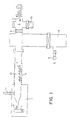
- FIG. 1 is a schematic representation of an ultra high vacuum CVD apparatus useful in the practice of the invention.
- FIG. 2 is an IR spectrum of the photoluminescent output of a device of the invention.
- a 7.6 cm diameter ultra high vacuum chemical vapor deposition (UHVCVD) reactor useful for the preparation of films of the invention is depicted in FIG. 1.
- the reactor differs in design from the original UHVCVD reactor described by Meyerson et al. in that pumping and wafer loading are done using the same end of the reactor. This modification allows the installation of a heated precursor reservoir 1 on the opposite end of the reactor.
- the reservoir is connected to the reactor end flange using a short length of 12.7 mm diameter stainless steel tubing 12.
- the reactor is constructed of quartz glass and stainless steel, using flanges, valves and seals common to the construction of high vacuum apparatus.
- the reactor is heated by external resistive heating (tube furnace 4).
- the reactor is pumped both before and during deposition by a 150 L/sec turbomolecular pump 8 backed by a two-stage oil pump 9.
- the load lock chamber is also pumped by a turbomolecular pump 10 to prevent contamination from pump oil.
- the base pressure of the reactor is below 133.3 10 ⁇ 9 Pa and the load lock is capable of producing pressures below 133.3 10 ⁇ 6 Pa from atmospheric pressure in less than 10 minutes.
- the precursor reservoir 1 is charged with an appropriate amount of the rare earth compound and evacuated.
- the rare earth is erbium, although other rare earths, particularly terbium and europium may also be used.
- the rare earths include elements 57 to 71.
- the rare earth compounds are restricted in that they must be able to provide a vapor for the CVD process at the temperatures and pressures at which CVD can be run. In a practical sense this means that the rare earth compound should exhibit a vapor pressure of at least about 10 ⁇ 6 torr at 500°C.
- Exemplary compounds fall into two broad categories: (a) coordination compounds, where the rare earth is bound to oxygen, nitrogen, sulfur or phosphorus, and (b) organometallic compounds, where the rare earth is bound to carbon atoms.
- suitable ligands for the coordination compounds include: acetylacetonate (2,4-pentanedionate) and derivatives of acetylacetonate including hexafluoroacetylacetonate (HFAC, 1,1,1,5,5,5-hexafluoro-2,4-pentanedionate) and trifluoroacetylacetonate (TFAC, 1,1,1-trifluoro-2,4-pentanedionate); 2,4-hexanedionate and derivatives of 2,4-hexanedionate; 2,4- and 3,5-heptanedionate and derivatives including 2,2,6,6-tetramethyl 3,5-heptanedionate (THD), 2,2,6-trimethyl 3,5-heptan
- organometallic compounds include tris-cyclopentadienyl erbium (III) and organic derivatives of the cyclopentadienyl ring including the tris-pentamethylcyclopentadienyl ligand, the methylcyclopentadienyl ligand, and the isopropylcyclopentadienyl ligand, bis(cyclopentadienyl)erbium halides, and bis-(cyclopentadienyl)erbium alkyls, wherein alkyl is defined as a linear or branched hydrocarbon radical of one to six carbon atoms.
- Preferred ligands include acetylacetonate, HFAC, THD and FOD.
- the substrate is loaded onto the quartz wafer boat 3, placed in the load-lock chamber 2 and evacuated to a suitable pressure, preferably less than 133.3 10 ⁇ 5 Pa.
- the substrate can be any material that is compatible with the CVD conditions; single-crystal silicon wafers are preferred. In general, a better film is produced when the substrate wafer has been previously cleaned in the usual manner.
- a precursor gas for the semiconductor film is introduced into the reactor.
- the precursor can be any silane or germane or mixture of the two that is volatile under the conditions of CVD; silane (SiH4), disilane (SI2H6), germane (GeH4) and digermane (Ge2H6) are preferred.
- Group III dopant precursors, such as diborane, or group V dopant precursors, such as phosphine, may be introduced to alter the electrical properties of the films.
- the semiconductor precursor gases are introduced via gas inlet 11 into the reactor.
- the temperature of the reactor is maintained at 450x to 800°C. Below 450° epitaxial growth of Si, Ge, or Si/Ge is not observed; as 900°C is approached, erbium begins to segregate.
- the pressure in the load- lock chamber 2 before introducing the substrate into the reactor is preferably below 133.3 10 ⁇ 5 Pa.
- the rare earth precursor is vaporized into the reaction chamber from the reservoir 1 by applying heat.
- the heat is supplied by an external oven 7 surrounding the reservoir.
- Er(HFAC)3 the optimal rate of vaporization is obtained when the oven is held at 58° C. Regulation of the precursor reservoir temperature, and hence regulation of the partial pressure of precursor in the reactor, is important to the success of the process.
- Er(HFAC) 3 at temperatures below 55°C, no erbium was incorporated. Above 65°C, the films consisted of a polycrystalline layer 30 to 40 nm thick with a concentration of erbium of 10 to 20%.
- This layer did not increase with longer deposition times, indicating that the growth surface was "poisoned" by the precursor.
- the likely explanation for this observation is that there is a minimum growth rate above which the erbium and other elements from the precursor may be incorporated and below which the growth surface is poisoned.
- the growth rate of pure silicon from silane at 1 mtorr pressure is 4 ⁇ /min at 550°C and 40 nm/min at 650°C.
- the selection of the appropriate oven temperature for a given rare earth compound is readily determined empirically as part of the routine adjustment of experimental conditions. Reasonable temperatures can be calculated by comparison of the vapor pressure of the precursor of interest at the pressure of the reservoir with the vapor pressure of Er(HFAC)3 at 58°/133.3 Pa.
- the precursor reservoir was charged with 1.0g of anhydrous tris(hexafluoroacetylacetonato-0,0') erbium (III) and evacuated.
- Anhydrous tris(hexafluoroacetylacetonato-0,0') erbium (III) was immediately placed in the reactor load-lock.
- the flow of silane (4 sccm) and hydrogen (50 sccm) was started, and the valve to the room-temperature erbium source was opened. After a ten minute pump down in the load-lock the wafers were transferred to the reactor. Three minutes after loading, the flow of hydrogen was stopped and the temperature of the reactor was increased from 500°C to 650°C over a period of one hour.
- the temperature of the oven surrounding the precursor was increased to 58°C, directly subliming Er(HFAC)3 into the reactor.
- the pressure during deposition was 200 Pa, giving a calculated system pumping speed of 42 L/sec.
- the deposition rate under these conditions was approximately 3 nm/min and deposition times varied from 3 to 12 hours.
- the flow of silane was discontinued, and the wafers were withdrawn to the load-lock chamber to cool.
- composition of the films was determined using Rutherford Back Scattering spectroscopy (RBS) to determine the erbium concentration and Secondary Ion Mass Spectroscopy (SIMS) to determine the level of carbon, fluorine and oxygen present in the films.
- the carbon, oxygen, and fluorine levels were equal in the three samples measured, within the uncertainty of the measurement. These "impurities" arise from the decomposition of the precursor.
- Sample 2 was a 2 ⁇ m thick film produced by lowering T e by 2°C and growing for longer time (11 h instead of 3 h). The cross sectional TEM of this film does not show any precipitated ErSi2.
- the erbium concentration of sample 2 was 2 x 10¹⁹ atoms/cm3. This level is at least one order of magnitude higher than the highest concentrations reported using implantation techniques.
- the cross-sectional TEM also shows a high density of threading defects. These defects may be due to stress caused by the introduction of erbium (or erbium complexes) into the film, but it is more likely that these defects are due to contamination from the precursor. At the temperatures used in UHVCVD, the crystal quality is very sensitive to the presence of carbon and oxygen and the SIMS results indicate that these elements are present in relatively high concentrations.
- One other possible source of contamination is residual carbon and oxygen from the decomposition of the ligand upstream from the deposition zone.
- the Er(HFAC)3 complex decomposes in parts of the reactor which are as much as 300°C cooler and may continue to evolve small quantities of organic material which may contaminate the initial growth surface. Support for this hypothesis is given by TEM which shows that the defects occur abruptly and at highest concentration at the initial growth interface. In this respect there may be an advantage to other precursors, particularly of the organometallic type, when used together with controlled levels of oxidant gas.
- Rare earth compounds can be prepared by methods well known in the art.
- the Er(HFAC)3 used in the foregoing experiment was made by a modification of the known process for the synthesis of Al(HFAC)3 described by Morris et al. in Inorganic Syntheses, Vol. 9, S.Y. Tyree, editor; McGraw Hill, New York, (1967) p. 39. This synthesis is an improvement over the synthesis of Er(HFAC)3 described by Berg and Acosta [Anal. Chim.
- Photoluminescence measurements were carried out on several of the samples. Measurements were done using an Ar ion laser operating at 514 nm as the excitation source and a Cygnus FTIR to detect the emitted radiation.
- a representative spectrum of a 2 ⁇ m film with an Er concentration of 2 x 10¹⁹ atoms/cm3 (identical to the sample used for TEM measurements above) is shown in FIG. 2. This spectrum was obtained at 10 K and the luminescence fell sharply as the temperature was raised. At 200 K, the signal intensity was down by a factor of 50 and was not observable at room temperature.
Landscapes
- Chemical Vapour Deposition (AREA)
- Crystals, And After-Treatments Of Crystals (AREA)
Applications Claiming Priority (2)
| Application Number | Priority Date | Filing Date | Title |
|---|---|---|---|
| US07/940,416 US5322813A (en) | 1992-08-31 | 1992-08-31 | Method of making supersaturated rare earth doped semiconductor layers by chemical vapor deposition |
| US940416 | 1992-08-31 |
Publications (3)
| Publication Number | Publication Date |
|---|---|
| EP0586321A2 true EP0586321A2 (de) | 1994-03-09 |
| EP0586321A3 EP0586321A3 (en) | 1996-03-27 |
| EP0586321B1 EP0586321B1 (de) | 1998-05-20 |
Family
ID=25474795
Family Applications (1)
| Application Number | Title | Priority Date | Filing Date |
|---|---|---|---|
| EP93480110A Expired - Lifetime EP0586321B1 (de) | 1992-08-31 | 1993-07-30 | Herstellung von dotierten, mit seltener Erde übersättigten Halbleiterschichten durch CVD |
Country Status (11)
| Country | Link |
|---|---|
| US (3) | US5322813A (de) |
| EP (1) | EP0586321B1 (de) |
| JP (1) | JPH0785467B2 (de) |
| KR (1) | KR970008339B1 (de) |
| CN (3) | CN1054234C (de) |
| AT (1) | ATE166491T1 (de) |
| CA (1) | CA2095449C (de) |
| DE (1) | DE69318653T2 (de) |
| ES (1) | ES2116426T3 (de) |
| MX (1) | MX9305267A (de) |
| TW (1) | TW229325B (de) |
Cited By (3)
| Publication number | Priority date | Publication date | Assignee | Title |
|---|---|---|---|---|
| WO2008000332A1 (de) * | 2006-06-29 | 2008-01-03 | Schmid Technology Systems Gmbh | Silizium-solarzellen mit lanthaniden zur veränderung des spektrums und verfahren zu deren herstellung |
| EP3027989A4 (de) * | 2013-07-30 | 2017-03-15 | Board of Regents, The University of Texas System | Probentransfer in einer hochvakuum-übergangsströmung |
| WO2020030900A1 (en) * | 2018-08-06 | 2020-02-13 | Queen Mary University Of London | Substrate layer |
Families Citing this family (33)
| Publication number | Priority date | Publication date | Assignee | Title |
|---|---|---|---|---|
| US4873549A (en) * | 1987-03-03 | 1989-10-10 | Mita Industrial Co., Ltd. | Device for detecting the life of an image forming process unit, opening of a seal of the unit and attachment of the unit to an image forming apparatus |
| EP0650200B1 (de) * | 1993-10-20 | 1999-03-10 | Consorzio per la Ricerca sulla Microelettronica nel Mezzogiorno | Elektrolumineszente Festkörpervorrichtung und Verfahren zu ihrer Herstellung |
| US6093246A (en) * | 1995-09-08 | 2000-07-25 | Sandia Corporation | Photonic crystal devices formed by a charged-particle beam |
| US5976941A (en) * | 1997-06-06 | 1999-11-02 | The Whitaker Corporation | Ultrahigh vacuum deposition of silicon (Si-Ge) on HMIC substrates |
| US6130471A (en) * | 1997-08-29 | 2000-10-10 | The Whitaker Corporation | Ballasting of high power silicon-germanium heterojunction biploar transistors |
| US6040225A (en) * | 1997-08-29 | 2000-03-21 | The Whitaker Corporation | Method of fabricating polysilicon based resistors in Si-Ge heterojunction devices |
| KR100377716B1 (ko) * | 1998-02-25 | 2003-03-26 | 인터내셔널 비지네스 머신즈 코포레이션 | 광학적 방사를 위해 희토류 원소로 도핑된 실리콘 구조체 및 방사방법 |
| WO2000000811A2 (en) * | 1998-06-29 | 2000-01-06 | San Diego State University Foundation | Method and apparatus for determination of carbon-halogen compounds and applications thereof |
| US6140669A (en) * | 1999-02-20 | 2000-10-31 | Ohio University | Gallium nitride doped with rare earth ions and method and structure for achieving visible light emission |
| US6143072A (en) * | 1999-04-06 | 2000-11-07 | Ut-Battelle, Llc | Generic process for preparing a crystalline oxide upon a group IV semiconductor substrate |
| US6255669B1 (en) * | 1999-04-23 | 2001-07-03 | The University Of Cincinnati | Visible light emitting device formed from wide band gap semiconductor doped with a rare earth element |
| KR100510996B1 (ko) * | 1999-12-30 | 2005-08-31 | 주식회사 하이닉스반도체 | 선택적 에피텍셜 성장 공정의 최적화 방법 |
| US6519543B1 (en) * | 2000-05-09 | 2003-02-11 | Agere Systems Inc. | Calibration method for quantitative elemental analysis |
| US6734453B2 (en) | 2000-08-08 | 2004-05-11 | Translucent Photonics, Inc. | Devices with optical gain in silicon |
| KR100384892B1 (ko) * | 2000-12-01 | 2003-05-22 | 한국전자통신연구원 | 에르븀이 도핑된 실리콘나노점의 형성 방법 |
| US6853447B2 (en) * | 2001-02-12 | 2005-02-08 | Analytical Spectral Devices, Inc. | System and method for the collection of spectral image data |
| US6894772B2 (en) * | 2001-02-12 | 2005-05-17 | Analytical Spectral Devices | System and method for grouping reflectance data |
| JP2002334868A (ja) * | 2001-05-10 | 2002-11-22 | Hitachi Kokusai Electric Inc | 基板処理装置および半導体装置の製造方法 |
| US20030111013A1 (en) * | 2001-12-19 | 2003-06-19 | Oosterlaken Theodorus Gerardus Maria | Method for the deposition of silicon germanium layers |
| US6771369B2 (en) * | 2002-03-12 | 2004-08-03 | Analytical Spectral Devices, Inc. | System and method for pharmacy validation and inspection |
| WO2004066345A2 (en) * | 2003-01-22 | 2004-08-05 | Group Iv Semiconductor Inc. | Doped semiconductor nanocrystal layers and preparation thereof |
| US7440180B2 (en) * | 2004-02-13 | 2008-10-21 | Tang Yin S | Integration of rare-earth doped amplifiers into semiconductor structures and uses of same |
| US7163878B2 (en) * | 2004-11-12 | 2007-01-16 | Texas Instruments Incorporated | Ultra-shallow arsenic junction formation in silicon germanium |
| CN100385693C (zh) * | 2005-08-18 | 2008-04-30 | 中国科学院半导体研究所 | 用等离子体处理提高硅基晶体薄膜发光的方法 |
| US20080138955A1 (en) * | 2006-12-12 | 2008-06-12 | Zhiyuan Ye | Formation of epitaxial layer containing silicon |
| JP5666433B2 (ja) * | 2008-06-05 | 2015-02-12 | レール・リキード−ソシエテ・アノニム・プール・レテュード・エ・レクスプロワタシオン・デ・プロセデ・ジョルジュ・クロード | ランタニド含有前駆体の調製およびランタニド含有膜の堆積 |
| US8269253B2 (en) * | 2009-06-08 | 2012-09-18 | International Rectifier Corporation | Rare earth enhanced high electron mobility transistor and method for fabricating same |
| CN102828242B (zh) * | 2012-09-06 | 2015-05-27 | 西安隆基硅材料股份有限公司 | 含有下转换发光量子点的晶体硅及其制备方法 |
| US9481917B2 (en) * | 2012-12-20 | 2016-11-01 | United Technologies Corporation | Gaseous based desulfurization of alloys |
| US9850573B1 (en) | 2016-06-23 | 2017-12-26 | Applied Materials, Inc. | Non-line of sight deposition of erbium based plasma resistant ceramic coating |
| US10364259B2 (en) * | 2016-12-30 | 2019-07-30 | L'Air Liquide, Société Anonyme pour l'Etude et l'Exploitation des Procédés Georges Claude | Zirconium, hafnium, titanium precursors and deposition of group 4 containing films using the same |
| US10975469B2 (en) | 2017-03-17 | 2021-04-13 | Applied Materials, Inc. | Plasma resistant coating of porous body by atomic layer deposition |
| CN119640395B (zh) * | 2025-02-13 | 2025-07-01 | 清华大学 | 二维单晶稀土化合物纳米片的制备方法 |
Family Cites Families (13)
| Publication number | Priority date | Publication date | Assignee | Title |
|---|---|---|---|---|
| DE1900116C3 (de) * | 1969-01-02 | 1978-10-19 | Siemens Ag, 1000 Berlin Und 8000 Muenchen | Verfahren zum Herstellen hxxochreiner, aus Silicium bestehender einkristalliner Schichten |
| US4385946A (en) * | 1981-06-19 | 1983-05-31 | Bell Telephone Laboratories, Incorporated | Rapid alteration of ion implant dopant species to create regions of opposite conductivity |
| US4618381A (en) * | 1983-05-26 | 1986-10-21 | Fuji Electric Corporate Research And Development Ltd. | Method for adding impurities to semiconductor base material |
| DE3319134A1 (de) * | 1983-05-26 | 1985-05-02 | Fraunhofer-Gesellschaft zur Förderung der angewandten Forschung e.V., 8000 München | Optoelektronisches bauelement, insbesondere eine laserdiode oder eine leuchtdiode |
| US4800173A (en) * | 1986-02-20 | 1989-01-24 | Canon Kabushiki Kaisha | Process for preparing Si or Ge epitaxial film using fluorine oxidant |
| US4826288A (en) * | 1987-04-09 | 1989-05-02 | Polaroid Corporation, Patent Department | Method for fabricating optical fibers having cores with high rare earth content |
| US5248890A (en) * | 1989-05-13 | 1993-09-28 | Forschungszentrum Julich Gmbh | Valance specific lanthanide doped optoelectronic metal fluoride semiconductor device |
| US5296048A (en) * | 1989-05-31 | 1994-03-22 | International Business Machines Corporation | Class of magnetic materials for solid state devices |
| FR2650704B1 (fr) * | 1989-08-01 | 1994-05-06 | Thomson Csf | Procede de fabrication par epitaxie de couches monocristallines de materiaux a parametres de mailles differents |
| JPH042699A (ja) * | 1990-04-18 | 1992-01-07 | Mitsubishi Electric Corp | 結晶成長方法 |
| US5119460A (en) * | 1991-04-25 | 1992-06-02 | At&T Bell Laboratories | Erbium-doped planar optical device |
| US5107538A (en) * | 1991-06-06 | 1992-04-21 | At&T Bell Laboratories | Optical waveguide system comprising a rare-earth Si-based optical device |
| US5511946A (en) * | 1994-12-08 | 1996-04-30 | General Electric Company | Cooled airfoil tip corner |
-
1992
- 1992-08-31 US US07/940,416 patent/US5322813A/en not_active Expired - Lifetime
-
1993
- 1993-05-04 CA CA002095449A patent/CA2095449C/en not_active Expired - Fee Related
- 1993-07-28 JP JP5185980A patent/JPH0785467B2/ja not_active Expired - Fee Related
- 1993-07-30 DE DE69318653T patent/DE69318653T2/de not_active Expired - Lifetime
- 1993-07-30 AT AT93480110T patent/ATE166491T1/de active
- 1993-07-30 ES ES93480110T patent/ES2116426T3/es not_active Expired - Lifetime
- 1993-07-30 EP EP93480110A patent/EP0586321B1/de not_active Expired - Lifetime
- 1993-08-19 TW TW082106685A patent/TW229325B/zh not_active IP Right Cessation
- 1993-08-30 KR KR1019930017032A patent/KR970008339B1/ko not_active Expired - Fee Related
- 1993-08-30 MX MX9305267A patent/MX9305267A/es not_active IP Right Cessation
- 1993-08-30 CN CN93117079A patent/CN1054234C/zh not_active Expired - Fee Related
-
1994
- 1994-03-09 US US08/207,942 patent/US5534079A/en not_active Expired - Lifetime
-
1995
- 1995-06-06 US US08/468,367 patent/US5646425A/en not_active Expired - Fee Related
-
1999
- 1999-11-09 CN CN99123481A patent/CN1117389C/zh not_active Expired - Fee Related
- 1999-11-09 CN CN99123482A patent/CN1114225C/zh not_active Expired - Fee Related
Cited By (3)
| Publication number | Priority date | Publication date | Assignee | Title |
|---|---|---|---|---|
| WO2008000332A1 (de) * | 2006-06-29 | 2008-01-03 | Schmid Technology Systems Gmbh | Silizium-solarzellen mit lanthaniden zur veränderung des spektrums und verfahren zu deren herstellung |
| EP3027989A4 (de) * | 2013-07-30 | 2017-03-15 | Board of Regents, The University of Texas System | Probentransfer in einer hochvakuum-übergangsströmung |
| WO2020030900A1 (en) * | 2018-08-06 | 2020-02-13 | Queen Mary University Of London | Substrate layer |
Also Published As
| Publication number | Publication date |
|---|---|
| MX9305267A (es) | 1994-02-28 |
| CN1085353A (zh) | 1994-04-13 |
| CN1255736A (zh) | 2000-06-07 |
| JPH0785467B2 (ja) | 1995-09-13 |
| CN1054234C (zh) | 2000-07-05 |
| US5534079A (en) | 1996-07-09 |
| KR970008339B1 (ko) | 1997-05-23 |
| CN1255735A (zh) | 2000-06-07 |
| EP0586321B1 (de) | 1998-05-20 |
| ES2116426T3 (es) | 1998-07-16 |
| DE69318653D1 (de) | 1998-06-25 |
| ATE166491T1 (de) | 1998-06-15 |
| JPH06177062A (ja) | 1994-06-24 |
| US5322813A (en) | 1994-06-21 |
| CN1117389C (zh) | 2003-08-06 |
| EP0586321A3 (en) | 1996-03-27 |
| CA2095449C (en) | 1997-09-16 |
| KR940004714A (ko) | 1994-03-15 |
| CN1114225C (zh) | 2003-07-09 |
| US5646425A (en) | 1997-07-08 |
| CA2095449A1 (en) | 1994-03-01 |
| TW229325B (de) | 1994-09-01 |
| DE69318653T2 (de) | 1999-02-04 |
Similar Documents
| Publication | Publication Date | Title |
|---|---|---|
| US5322813A (en) | Method of making supersaturated rare earth doped semiconductor layers by chemical vapor deposition | |
| US5124278A (en) | Amino replacements for arsine, antimony and phosphine | |
| EP0179138B1 (de) | Ein verfahren zur herstellung einer verbindungshalbleiterstruktur | |
| US5296258A (en) | Method of forming silicon carbide | |
| US4904616A (en) | Method of depositing arsine, antimony and phosphine substitutes | |
| Kuech et al. | Disilane: A new silicon doping source in metalorganic chemical vapor deposition of GaAs | |
| US5300185A (en) | Method of manufacturing III-V group compound semiconductor | |
| US4988640A (en) | Method of doping and implanting using arsine, antimony, and phosphine substitutes | |
| US3836408A (en) | Production of epitaxial films of semiconductor compound material | |
| Gun'ko et al. | Organolanthanides in materials science | |
| US5410178A (en) | Semiconductor films | |
| Rogers et al. | Erbium‐doped silicon films grown by plasma‐enhanced chemical‐vapor deposition | |
| JP3399642B2 (ja) | 半導体発光素子層の形成方法 | |
| Beach et al. | Erbium-Doped Silicon Prepared by UHV/CVD | |
| Greenwald et al. | Mocvd Erbium Sourcesa | |
| US7329554B2 (en) | Reactive codoping of GaAlInP compound semiconductors | |
| JPS60169563A (ja) | テルル化金属の製造方法及び装置 | |
| US5306660A (en) | Technique for doping mercury cadmium telluride MOCVD grown crystalline materials using free radical transport of elemental indium and apparatus therefor | |
| Smith | Epitaxial growth of GaAs by low-pressure MOCVD | |
| JP3441534B2 (ja) | 結晶性シリコンの形成方法 | |
| CA1210526A (en) | Device having semi-insulating indium phosphides based compositions | |
| Andry et al. | Low-Temperature Growth of Si: Er by Electron Cyclotron Resonance Pecvd Using Metal Organics | |
| Hahn | Direct growth of mercury (1-x) cadmium (x) telluride by cold wall, pyrolytic OMVPE | |
| Vrahue | Low Temperature Epitaxial Growth of Rare Earth Doped Silicon and Silicon Germanium Alloys. | |
| Babushkina et al. | Effects of growth conditions on the photoluminescence spectra of epitaxial GaAs films made by the hydride method |
Legal Events
| Date | Code | Title | Description |
|---|---|---|---|
| PUAI | Public reference made under article 153(3) epc to a published international application that has entered the european phase |
Free format text: ORIGINAL CODE: 0009012 |
|
| AK | Designated contracting states |
Kind code of ref document: A2 Designated state(s): AT BE CH DE ES FR GB IT LI NL SE |
|
| 17P | Request for examination filed |
Effective date: 19940627 |
|
| PUAL | Search report despatched |
Free format text: ORIGINAL CODE: 0009013 |
|
| AK | Designated contracting states |
Kind code of ref document: A3 Designated state(s): AT BE CH DE ES FR GB IT LI NL SE |
|
| 17Q | First examination report despatched |
Effective date: 19960603 |
|
| GRAG | Despatch of communication of intention to grant |
Free format text: ORIGINAL CODE: EPIDOS AGRA |
|
| RTI1 | Title (correction) | ||
| GRAG | Despatch of communication of intention to grant |
Free format text: ORIGINAL CODE: EPIDOS AGRA |
|
| GRAH | Despatch of communication of intention to grant a patent |
Free format text: ORIGINAL CODE: EPIDOS IGRA |
|
| GRAH | Despatch of communication of intention to grant a patent |
Free format text: ORIGINAL CODE: EPIDOS IGRA |
|
| GRAA | (expected) grant |
Free format text: ORIGINAL CODE: 0009210 |
|
| AK | Designated contracting states |
Kind code of ref document: B1 Designated state(s): AT BE CH DE ES FR GB IT LI NL SE |
|
| REF | Corresponds to: |
Ref document number: 166491 Country of ref document: AT Date of ref document: 19980615 Kind code of ref document: T |
|
| REG | Reference to a national code |
Ref country code: CH Ref legal event code: NV Representative=s name: CARL O. BARTH C/O IBM CORPORATION ZURICH INTELLECT Ref country code: CH Ref legal event code: EP |
|
| REF | Corresponds to: |
Ref document number: 69318653 Country of ref document: DE Date of ref document: 19980625 |
|
| REG | Reference to a national code |
Ref country code: ES Ref legal event code: FG2A Ref document number: 2116426 Country of ref document: ES Kind code of ref document: T3 |
|
| ITF | It: translation for a ep patent filed | ||
| ET | Fr: translation filed | ||
| PGFP | Annual fee paid to national office [announced via postgrant information from national office to epo] |
Ref country code: CH Payment date: 19981027 Year of fee payment: 6 |
|
| PLBE | No opposition filed within time limit |
Free format text: ORIGINAL CODE: 0009261 |
|
| STAA | Information on the status of an ep patent application or granted ep patent |
Free format text: STATUS: NO OPPOSITION FILED WITHIN TIME LIMIT |
|
| 26N | No opposition filed | ||
| PGFP | Annual fee paid to national office [announced via postgrant information from national office to epo] |
Ref country code: AT Payment date: 19990729 Year of fee payment: 7 |
|
| PG25 | Lapsed in a contracting state [announced via postgrant information from national office to epo] |
Ref country code: LI Free format text: LAPSE BECAUSE OF NON-PAYMENT OF DUE FEES Effective date: 19990731 Ref country code: CH Free format text: LAPSE BECAUSE OF NON-PAYMENT OF DUE FEES Effective date: 19990731 |
|
| REG | Reference to a national code |
Ref country code: CH Ref legal event code: PL |
|
| PG25 | Lapsed in a contracting state [announced via postgrant information from national office to epo] |
Ref country code: AT Free format text: LAPSE BECAUSE OF NON-PAYMENT OF DUE FEES Effective date: 20000730 |
|
| PGFP | Annual fee paid to national office [announced via postgrant information from national office to epo] |
Ref country code: BE Payment date: 20000807 Year of fee payment: 8 |
|
| PG25 | Lapsed in a contracting state [announced via postgrant information from national office to epo] |
Ref country code: BE Free format text: LAPSE BECAUSE OF NON-PAYMENT OF DUE FEES Effective date: 20010731 |
|
| REG | Reference to a national code |
Ref country code: GB Ref legal event code: IF02 |
|
| BERE | Be: lapsed |
Owner name: INTERNATIONAL BUSINESS MACHINES CORP. Effective date: 20010731 |
|
| PGFP | Annual fee paid to national office [announced via postgrant information from national office to epo] |
Ref country code: FR Payment date: 20020715 Year of fee payment: 10 |
|
| PG25 | Lapsed in a contracting state [announced via postgrant information from national office to epo] |
Ref country code: FR Free format text: LAPSE BECAUSE OF NON-PAYMENT OF DUE FEES Effective date: 20040331 |
|
| REG | Reference to a national code |
Ref country code: FR Ref legal event code: ST |
|
| PGFP | Annual fee paid to national office [announced via postgrant information from national office to epo] |
Ref country code: IT Payment date: 20060731 Year of fee payment: 14 |
|
| REG | Reference to a national code |
Ref country code: GB Ref legal event code: 746 Effective date: 20080704 |
|
| PGFP | Annual fee paid to national office [announced via postgrant information from national office to epo] |
Ref country code: ES Payment date: 20080707 Year of fee payment: 16 |
|
| PGFP | Annual fee paid to national office [announced via postgrant information from national office to epo] |
Ref country code: NL Payment date: 20080731 Year of fee payment: 16 |
|
| PG25 | Lapsed in a contracting state [announced via postgrant information from national office to epo] |
Ref country code: IT Free format text: LAPSE BECAUSE OF NON-PAYMENT OF DUE FEES Effective date: 20070730 |
|
| PGFP | Annual fee paid to national office [announced via postgrant information from national office to epo] |
Ref country code: SE Payment date: 20090730 Year of fee payment: 17 |
|
| NLV4 | Nl: lapsed or anulled due to non-payment of the annual fee |
Effective date: 20100201 |
|
| REG | Reference to a national code |
Ref country code: ES Ref legal event code: FD2A Effective date: 20090731 |
|
| PG25 | Lapsed in a contracting state [announced via postgrant information from national office to epo] |
Ref country code: ES Free format text: LAPSE BECAUSE OF NON-PAYMENT OF DUE FEES Effective date: 20090731 |
|
| PG25 | Lapsed in a contracting state [announced via postgrant information from national office to epo] |
Ref country code: NL Free format text: LAPSE BECAUSE OF NON-PAYMENT OF DUE FEES Effective date: 20100201 Ref country code: SE Free format text: LAPSE BECAUSE OF NON-PAYMENT OF DUE FEES Effective date: 20100731 |
|
| PGFP | Annual fee paid to national office [announced via postgrant information from national office to epo] |
Ref country code: GB Payment date: 20120723 Year of fee payment: 20 |
|
| PGFP | Annual fee paid to national office [announced via postgrant information from national office to epo] |
Ref country code: DE Payment date: 20120723 Year of fee payment: 20 |
|
| REG | Reference to a national code |
Ref country code: DE Ref legal event code: R071 Ref document number: 69318653 Country of ref document: DE |
|
| REG | Reference to a national code |
Ref country code: DE Ref legal event code: R071 Ref document number: 69318653 Country of ref document: DE |
|
| REG | Reference to a national code |
Ref country code: GB Ref legal event code: PE20 Expiry date: 20130729 |
|
| PG25 | Lapsed in a contracting state [announced via postgrant information from national office to epo] |
Ref country code: DE Free format text: LAPSE BECAUSE OF EXPIRATION OF PROTECTION Effective date: 20130731 |
|
| PG25 | Lapsed in a contracting state [announced via postgrant information from national office to epo] |
Ref country code: GB Free format text: LAPSE BECAUSE OF EXPIRATION OF PROTECTION Effective date: 20130729 |
|
| REG | Reference to a national code |
Ref country code: DE Ref legal event code: R081 Ref document number: 69318653 Country of ref document: DE Owner name: GLOBALFOUNDRIES INC., KY Free format text: FORMER OWNER: INTERNATIONAL BUSINESS MACHINES CORPORATION, ARMONK, NY, US Ref country code: DE Ref legal event code: R082 Ref document number: 69318653 Country of ref document: DE Representative=s name: RICHARDT PATENTANWAELTE PARTG MBB, DE Ref country code: DE Ref legal event code: R081 Ref document number: 69318653 Country of ref document: DE Owner name: GLOBALFOUNDRIES INC., KY Free format text: FORMER OWNER: INTERNATIONAL BUSINESS MACHINES CORPORATION, ARMONK, N.Y., US |
|
| REG | Reference to a national code |
Ref country code: DE Ref legal event code: R082 Ref document number: 69318653 Country of ref document: DE Representative=s name: RICHARDT PATENTANWAELTE PARTG MBB, DE Ref country code: DE Ref legal event code: R081 Ref document number: 69318653 Country of ref document: DE Owner name: GLOBALFOUNDRIES INC., KY Free format text: FORMER OWNER: GLOBALFOUNDRIES US 2 LLC (N.D.GES.DES STAATES DELAWARE), HOPEWELL JUNCTION, N.Y., US |
|
| REG | Reference to a national code |
Ref country code: FR Ref legal event code: TP Owner name: GLOBALFOUNDRIES INC., GB Effective date: 20160829 |