EP0585050A2 - Multi-mode frequency synthesiser with reduced jitter - Google Patents
Multi-mode frequency synthesiser with reduced jitter Download PDFInfo
- Publication number
- EP0585050A2 EP0585050A2 EP93306545A EP93306545A EP0585050A2 EP 0585050 A2 EP0585050 A2 EP 0585050A2 EP 93306545 A EP93306545 A EP 93306545A EP 93306545 A EP93306545 A EP 93306545A EP 0585050 A2 EP0585050 A2 EP 0585050A2
- Authority
- EP
- European Patent Office
- Prior art keywords
- frequency
- phase
- clock signal
- signal
- locked loop
- Prior art date
- Legal status (The legal status is an assumption and is not a legal conclusion. Google has not performed a legal analysis and makes no representation as to the accuracy of the status listed.)
- Withdrawn
Links
Images

Classifications
-
- H—ELECTRICITY
- H03—ELECTRONIC CIRCUITRY
- H03L—AUTOMATIC CONTROL, STARTING, SYNCHRONISATION OR STABILISATION OF GENERATORS OF ELECTRONIC OSCILLATIONS OR PULSES
- H03L7/00—Automatic control of frequency or phase; Synchronisation
- H03L7/06—Automatic control of frequency or phase; Synchronisation using a reference signal applied to a frequency- or phase-locked loop
- H03L7/16—Indirect frequency synthesis, i.e. generating a desired one of a number of predetermined frequencies using a frequency- or phase-locked loop
- H03L7/22—Indirect frequency synthesis, i.e. generating a desired one of a number of predetermined frequencies using a frequency- or phase-locked loop using more than one loop
- H03L7/23—Indirect frequency synthesis, i.e. generating a desired one of a number of predetermined frequencies using a frequency- or phase-locked loop using more than one loop with pulse counters or frequency dividers
- H03L7/235—Nested phase locked loops
Definitions
- This invention relates to a frequency synthesizer, more specifically to a frequency synthesizer that receives an input clock signal and generates a stable output clock signal at any of several selectable frequencies.
- a frequency synthesizer is in a television receiver that converts a high-definition television signal (HDTV signal) to a standard television signal for display on a standard-size television screen.
- HDTV signal high-definition television signal
- the demand for receivers equipped to make this conversion is expected to be strong while conventional TV and HDTV coexist, as they already do in Japan and soon will in other countries.
- the conversion can be carried out in several modes, requiring stable clock signals of different frequencies. To give the viewer a choice of modes, it is desirable for a single frequency synthesizer to be able to synthesize all the necessary clock frequencies.
- a frequency synthesizer is conventionally configured as a phase-locked loop (PLL) comprising a phase comparator, a loop filter, and a voltage-controlled oscillator (VCO) coupled in series.
- PLL phase-locked loop
- VCO voltage-controlled oscillator
- the phase comparator receives an input signal and the VCO generates an output signal, which is also fed back to the phase comparator.
- Different output frequencies can be obtained by appropriate division of the input and feedback signals.
- the loop filter is an active low-pass filter employing an operational amplifier
- the VCO is a voltage-controlled multivibrator.
- frequency synthesizers of this design tend to suffer from output jitter.
- An active filter employing an operational amplifier, particularly a filter small enough to form part of an integrated circuit cannot adequately reject all the high frequencies occurring in the output of the phase comparator in different modes.
- a voltage-controlled multivibrator does not possess inherently high frequency stability, so the unrejected high frequencies can easily disturb the output.
- an LC oscillator circuit comprising an inductor and a capacitor that resonate at a particular frequency. Different output frequencies are obtained by switching among different capacitors.
- the circuit can no longer be satisfactorily integrated; the inductor, capacitors, and switch must all be external components.
- the switch is particularly inconvenient because it requires bulky mechanical contacts in order to obtain low on-resistance.
- the invented frequency synthesizer comprises a pair of cascaded phase-locked loops.
- the first phase-locked loop receives an input clock signal and a first feedback signal and generates an internal clock signal.
- the second phase-locked loop receives the internal clock signal and a second feedback signal and generates an output clock signal.
- the output clock signal is supplied to both the first and second phase-locked loops for use as the first and second feedback signals.
- the first phase-locked loop has programmable frequency dividers for dividing the frequencies of the input clock signal and first feedback signal.
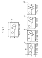
- Fig. 1 is a sketch illustrating different modes for converting an HDTV picture to a standard TV picture.
- Fig. 2 is a block diagram of a television signal converter, illustrating a type of circuit in which the invented frequency synthesizer can be advantageously used.
- Fig. 3 is a block diagram of the invented frequency synthesizer.
- Figs. 1 and 2 illustrate one of the purposes for which the invention can be used, although applications of the invention are not limited to this purpose.
- Fig. 3 illustrates an embodiment of the invention, although the scope of the invention, as set forth in the appended claims, is not restricted to this embodiment.
- Fig. 1 shows four modes in which an HDTV picture 2 can be displayed on a conventional television screen.
- the HDTV picture has a 9:16 aspect ratio with, for example, 1125 horizontal scanning lines, while the conventional screen has a 3:4 (i.e. 9:12) aspect ratio with, for example, 525 scanning lines.
- the 1/3 wide mode 4 three HDTV scanning lines are combined into one conventional scanning line.
- the resulting picture is displayed on a central band of the conventional screen, with substantially the same aspect ratio as the HDTV picture.
- the 2/5 wide scanning mode 6 five HDTV scanning lines are combined into two conventional scanning lines.
- the resulting picture is displayed on a taller central band of the conventional screen, altering the aspect ratio so that objects appear somewhat squeezed horizontally.
- zoom mode 8 the right and left side portions of the HDTV picture are discarded to make the picture fit the conventional screen without squeezing.
- full mode 10 the entire HDTV picture is displayed on the entire conventional screen, with considerable squeezing.
- Table 1 lists parameters of the conventional and HDTV systems employed in Japan.
- the HDTV system named MUSE, is an analog system developed by Japan's national broadcasting association (NHK).
- the conventional system is the well-known NTSC system developed by the National Television System Committee in the United States.
- EDTV extended-definition television
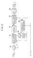
- Fig. 2 illustrates a picture converter capable of converting an analog HDTV signal such as a MUSE signal to a conventional NTSC signal.
- the HDTV signal is input to an analog-to-digital (A/D) converter 12, converted to a digital signal, and processed by an HDTV signal processor 14.
- the resulting data are written into a memory 16 at a clock rate F i .
- the data are then read from the memory 16 at a different clock rate F o by an NTSC signal processor 18, and processed to produce a digital luminance signal Y and digital color difference signals R - Y and B - Y.
- D/A digital-to-analog
- the HDTV signal processor 14 sends a digital control signal to a D/A converter 22, and the resulting analog control signal is applied to a voltage-controlled crystal oscillator (VCXO) 24.
- the output of the VCXO 24 is a clock signal with frequency f i .
- Input to the HDTV signal processor 14, this f i clock signal generates both the F i write clock and an F i sampling clock furnished to the A/D converter 12.
- the VCXO 24 is adapted to oscillate at 32.4 MHZ.
- the HDTV signal processor 14 controls the VCXO 24 by slightly varying the oscillation rate so as to hold F i at precisely 960/2 times the horizontal scanning frequency, thereby keeping F i in accurate synchronization with the HDTV input signal.
- the HDTV horizontal scanning frequency is 33.750 kHz, so F i is 16.2 MHz.
- the f i clock signal from the VCXO 24 is also input to a frequency synthesizer 26, together with a mode control signal having four states, denoted m1 to m4.
- the frequency synthesizer 26 generates an output clock signal with a frequency f o that depends on the mode control signal. Although the f i and f o frequencies differ, the frequency synthesizer 26 keeps the f i input clock and f o output clock precisely synchronized, so that memory reading and writing will stay in step.
- the required output frequency f o depends on the mode in which the NTSC signal is generated from the HDTV signal. For example, the full mode shown in Fig. 1 requires a higher frequency than the zoom mode, because the latter reads only part of the data in each HDTV scanning line.
- Table 2 lists the f i and f o frequencies for the four modes shown in Fig. 1, assuming the signal parameters in Table 1.
- Fig. 3 shows the invented frequency synthesizer, which can be advantageously used in Fig. 2 to generate the output clock f o from the input clock f i according to the mode control signal.
- a first frequency divider 28 divides the input signal f i by a ratio N to create a signal f r .
- a second frequency divider 30 divides the output signal f o by another ratio M to create a feedback signal f r1 .
- a first phase comparator 32 receives f r and f r1 and generates a first error voltage v1 responsive to the frequency and phase difference between f r and f r1 .
- a first low-pass filter (LPF) 34 removes high- frequency components from the error voltage v1.
- the output of the LPF 34 is applied to a first voltaage-controlled oscillator (VCO) 36, which generates an internal clock signal f x .
- the internal clock frequency f x is constant, so the first VCO 36 can be an oscillator with high frequency stability, preferably a voltage-controlled crystal oscillator (VCXO).
- a third frequency divider 38 divides the internal clock signal f x by a ratio P to create a signal f s .
- a fourth frequency divider 40 divides the output signal f o by another ratio Q to create a feedback signal f s1 .
- a second phase comparator 42 receives f s and f s1 and generates a second error voltage v2 responsive to the frequency and phase difference between f s and f s1 .
- a second LPF 44 removes high-frequency components from the error voltage v2. The output of the LPF 44 is applied to a second VCO 46, which generates the output signal f o .
- the second VCO 46 is, for example, a voltage-controlled multivibrator capable of oscillating at all of the output frequencies f o listed in Table 1.
- the first, second, third, and fourth frequency dividers 28, 30, 38, and 40 are programmable frequency dividers that are controlled by the mode control signal, which takes on values m1, m2, m3, and m4 to select the four modes listed in Table 2.
- the values of N, M, P, and Q vary depending on the selected mode.
- the first and second LPFs 34 and 44 are, for example, low-pass filters of the well-known RC type, comprising resistor-capacitor networks.
- the invention is not limited to the use of RC filters as the low-pass filters 34 and 44.
- a voltage-controlled crystal oscillator as the first VCO 36, or a voltage-controlled multivibrator as the second VCO 46.
- the invention can obviously be practiced with other types of filters and oscillators.
- the circuit in Fig. 3 can be viewed as a pair of cascaded phase-locked loops (PLLs) 48 and 50 in which the output of the second PLL 50 is fed back to both the first and second PLLs.
- the first PLL 48 comprises the first and second frequency dividers 28 and 30, the first phase comparator 32, the first LPF 34, and the first VCO 36.
- the second PLL 50 comprises the third and fourth frequency dividers 38 and 40, the second phase comparator 42, the second LPF 44, and the second VCO 46.
- the second PLL 50 operates so as to lock f s1 to f s in frequency and phase.
- the circuit in Fig. 3 can be viewed as a pair of nested PLLs, the inner PLL functioning as the loop filter of the outer PLL.
- the inner PLL comprises the first LPF 34, the first VCO 36, the third and fourth frequency dividers 38 and 40, the second phase comparator 42, and the second LPF 44.
- the outer PLL comprises the first and second frequency dividers 28 and 30, the first phase comparator 32, and the second VCO 46.
- the outer PLL operates so as to lock f r1 to f r in frequency and phase, thereby also keeping f o accurately synchronized to f i
- Equation (1) can be used to determine suitable integer values for M and N from f i and f o in each mode.
- Equation (2) or (3) can be used to determine integer values for P and Q.
- f x has a fixed value equal to the oscillating frequency of the first VCO 36 when the first error voltage v1 is, for example, zero.
- Table 3 shows a suitable set of values for N, M, P, and Q when f x is 1.89 MHz. Also shown in Table 3 are the values of f i , f o , f r , and f s . It can be readily verified that these parameters satisfy equations (1) to (3), from which it follows that the frequency synthesizer will lock at the desired output frequency f o in each mode.
- the first LPF 34 must reject f r and its harmonics.
- f r is 0.135 MHz in modes m2 and m4, 0.72 MHz in mode m1, and 0.9 MHz in mode m3, varying by a factor of more than six. If the cutoff frequency of the first LPF 34 is set high enough for satisfactory operation in modes m1 and m3, the LPF 34 will fail to reject all the high-frequency components occurring in modes m2 and m4. Because of the stability of the first VCO 36, however, the remaining high-frequency components in the first error voltage v1 can be tolerated; the output frequency f x of the VCO 36 is substantially unaffected by them.
- the second LPF 44 must reject f s and its harmonics.
- f s is 0.63 MHz in modes m1 and m3 and 0.945 MHz in modes m2 and m4, varying by a factor of only one and one-half.
- the second LPF 44 can be designed to reject both 0.63-MHz and 0.945-MHz components adequately without impairing loop performance. Accordingly, even if the second VCO 46 is not inherently stable, it can produce a jitter-free output frequency f o because the error voltage v2 is free of high-frequency noise.
- the invented frequency synthesizer can easily be fabricated as an integrated circuit, or as part of an integrated circuit, requiring only a crystal and a few resistors and capacitors as external components. Jitter-free output is obtained without the need for a bulky external mechanical switch.
- N, M, P, Q, and f x can be varied according to the requirements of different television systems.
- f x is no longer constant; it becomes equal to f o , so the first VCO 36 must oscillate at the same frequencies as the second VCO 46.
- a voltage-controlled multivibrator or other type of oscillator must be used for the first VCO 36.
- the invention succeeds in reducing output jitter. Since f s also becomes equal to f o , the frequencies to be rejected by the second LPF 44 again vary by a factor of only about one and one-half, and the second LPF 44 can be designed to reject all of them adequately.
Landscapes
- Stabilization Of Oscillater, Synchronisation, Frequency Synthesizers (AREA)
- Synchronizing For Television (AREA)
- Television Systems (AREA)
Applications Claiming Priority (2)
| Application Number | Priority Date | Filing Date | Title |
|---|---|---|---|
| JP4224445A JPH0677823A (ja) | 1992-08-24 | 1992-08-24 | 周波数シンセサイザ |
| JP224445/92 | 1992-08-24 |
Publications (2)
| Publication Number | Publication Date |
|---|---|
| EP0585050A2 true EP0585050A2 (en) | 1994-03-02 |
| EP0585050A3 EP0585050A3 (OSRAM) | 1994-04-13 |
Family
ID=16813888
Family Applications (1)
| Application Number | Title | Priority Date | Filing Date |
|---|---|---|---|
| EP93306545A Withdrawn EP0585050A2 (en) | 1992-08-24 | 1993-08-19 | Multi-mode frequency synthesiser with reduced jitter |
Country Status (2)
| Country | Link |
|---|---|
| EP (1) | EP0585050A2 (OSRAM) |
| JP (1) | JPH0677823A (OSRAM) |
Cited By (8)
| Publication number | Priority date | Publication date | Assignee | Title |
|---|---|---|---|---|
| DE19734656A1 (de) * | 1997-08-11 | 1999-02-18 | Alsthom Cge Alcatel | Schaltungsanordnung zur Einstellung einer Systemfrequenz |
| WO1999008384A3 (en) * | 1997-08-12 | 1999-04-29 | Koninkl Philips Electronics Nv | Multichannel radio device, a radio communication system, and a fractional division frequency synthesizer |
| WO2000057555A1 (de) * | 1999-03-23 | 2000-09-28 | Infineon Technologies Ag | Frequenzsynthesizer |
| EP0971491A4 (en) * | 1997-03-28 | 2002-04-10 | Rohm Co Ltd | IRDA INTEGRATED MODULATOR / DEMODULATOR CIRCUIT |
| EP1107458A3 (en) * | 1999-12-07 | 2004-03-10 | The Boeing Company | System for limiting IF variation in phase locked loops |
| EP1313256A3 (en) * | 2001-11-14 | 2006-05-17 | Mitsubishi Denki Kabushiki Kaisha | Data clock regenerating apparatus |
| US9948450B2 (en) | 2006-03-14 | 2018-04-17 | Intel Deutschland Gmbh | Frequency generator |
| EP2554015B1 (en) | 2010-03-31 | 2018-10-17 | CommScope Technologies LLC | Synchronous transfer of streaming data in a distributed antenna system |
Families Citing this family (4)
| Publication number | Priority date | Publication date | Assignee | Title |
|---|---|---|---|---|
| JP4686432B2 (ja) * | 2006-10-13 | 2011-05-25 | 三菱電機株式会社 | クロック位相シフト装置 |
| JP2009016973A (ja) * | 2007-07-02 | 2009-01-22 | Japan Radio Co Ltd | シンセサイザ |
| US8432151B2 (en) | 2008-09-22 | 2013-04-30 | Pioneer Corporation | Film-thickness measuring device using PLL circuit |
| KR20130015924A (ko) * | 2011-08-05 | 2013-02-14 | 주식회사 아이덴코아 | 위상 고정 루프 및 이를 포함하는 클럭 발생 시스템 |
Family Cites Families (2)
| Publication number | Priority date | Publication date | Assignee | Title |
|---|---|---|---|---|
| US4180783A (en) * | 1977-09-06 | 1979-12-25 | Rca Corporation | Phase lock loop data timing recovery circuit |
| JPS63128816A (ja) * | 1986-11-18 | 1988-06-01 | Toshiba Corp | Pll回路 |
-
1992
- 1992-08-24 JP JP4224445A patent/JPH0677823A/ja active Pending
-
1993
- 1993-08-19 EP EP93306545A patent/EP0585050A2/en not_active Withdrawn
Cited By (13)
| Publication number | Priority date | Publication date | Assignee | Title |
|---|---|---|---|---|
| EP0971491A4 (en) * | 1997-03-28 | 2002-04-10 | Rohm Co Ltd | IRDA INTEGRATED MODULATOR / DEMODULATOR CIRCUIT |
| US6526270B1 (en) | 1997-03-28 | 2003-02-25 | Rohm Co., Ltd. | IrDA modulation/demodulation integrated circuit device |
| DE19734656A1 (de) * | 1997-08-11 | 1999-02-18 | Alsthom Cge Alcatel | Schaltungsanordnung zur Einstellung einer Systemfrequenz |
| WO1999008384A3 (en) * | 1997-08-12 | 1999-04-29 | Koninkl Philips Electronics Nv | Multichannel radio device, a radio communication system, and a fractional division frequency synthesizer |
| US6611175B2 (en) | 1999-03-23 | 2003-08-26 | Infineon Technologies Ag | Frequency synthesizer and method of providing a mixing oscillator signal to a mixer |
| DE19913110C1 (de) * | 1999-03-23 | 2000-11-16 | Siemens Ag | Frequenzsynthesizer |
| WO2000057555A1 (de) * | 1999-03-23 | 2000-09-28 | Infineon Technologies Ag | Frequenzsynthesizer |
| EP1107458A3 (en) * | 1999-12-07 | 2004-03-10 | The Boeing Company | System for limiting IF variation in phase locked loops |
| EP1313256A3 (en) * | 2001-11-14 | 2006-05-17 | Mitsubishi Denki Kabushiki Kaisha | Data clock regenerating apparatus |
| US9948450B2 (en) | 2006-03-14 | 2018-04-17 | Intel Deutschland Gmbh | Frequency generator |
| EP2554015B1 (en) | 2010-03-31 | 2018-10-17 | CommScope Technologies LLC | Synchronous transfer of streaming data in a distributed antenna system |
| US10461919B2 (en) | 2010-03-31 | 2019-10-29 | Commscope Technologies Llc | Synchronous transfer of streaming data in a distributed antenna system |
| EP2554015B2 (en) † | 2010-03-31 | 2022-03-02 | CommScope Technologies LLC | Synchronous transfer of streaming data in a distributed antenna system |
Also Published As
| Publication number | Publication date |
|---|---|
| JPH0677823A (ja) | 1994-03-18 |
| EP0585050A3 (OSRAM) | 1994-04-13 |
Similar Documents
| Publication | Publication Date | Title |
|---|---|---|
| US6888580B2 (en) | Integrated single and dual television tuner having improved fine tuning | |
| EP0644657B1 (en) | Phase-locked oscillator circuit | |
| EP0585050A2 (en) | Multi-mode frequency synthesiser with reduced jitter | |
| JPH09162730A (ja) | Pll回路 | |
| EP0432052B1 (en) | RF modulator | |
| US5574515A (en) | Voltage controlled oscillator circuit and automatic fine tuning circuit for TV | |
| US20040207476A1 (en) | PLL circuit and television receiver having same and beat reducing method for television receiver | |
| US5036293A (en) | Oscillator for use with video signal time scaling apparatus | |
| JPS62159981A (ja) | ビデオ装置用同期回路 | |
| JPH11514830A (ja) | 電荷ポンプを有する周波数合成回路 | |
| EP0718979B1 (en) | Television standard discrimination circuit | |
| US5943098A (en) | Television image format non-linear conversion device | |
| US6650375B1 (en) | Television signal transmitter for eliminating interference caused by differential signal of two frequency converters | |
| KR970009066B1 (ko) | 위상 로크 루프 시스템 | |
| JP3277160B2 (ja) | Pal方式の同期信号発生回路 | |
| CN1777035B (zh) | 振荡器、集成电路、通信装置 | |
| JPH06291644A (ja) | Pll回路 | |
| JP3322534B2 (ja) | Rfモジュレータ | |
| KR910009089B1 (ko) | Pll 회로 | |
| JP2609936B2 (ja) | Muse/ntscコンバータ | |
| JPS6070888A (ja) | Vtrカメラ用信号発生装置 | |
| JP2622759B2 (ja) | Pll回路 | |
| JPH06291651A (ja) | 液晶表示装置用pll回路 | |
| JPH0568182A (ja) | 映像信号のサンプリングクロツク発生装置 | |
| JPH0716161B2 (ja) | Pll回路 |
Legal Events
| Date | Code | Title | Description |
|---|---|---|---|
| PUAI | Public reference made under article 153(3) epc to a published international application that has entered the european phase |
Free format text: ORIGINAL CODE: 0009012 |
|
| PUAL | Search report despatched |
Free format text: ORIGINAL CODE: 0009013 |
|
| AK | Designated contracting states |
Kind code of ref document: A2 Designated state(s): DE FR NL |
|
| AK | Designated contracting states |
Kind code of ref document: A3 Designated state(s): DE FR NL |
|
| STAA | Information on the status of an ep patent application or granted ep patent |
Free format text: STATUS: THE APPLICATION IS DEEMED TO BE WITHDRAWN |
|
| 18D | Application deemed to be withdrawn |
Effective date: 19941014 |