EP0581889B1 - Generating electric power from solar radiation - Google Patents
Generating electric power from solar radiation Download PDFInfo
- Publication number
- EP0581889B1 EP0581889B1 EP92912817A EP92912817A EP0581889B1 EP 0581889 B1 EP0581889 B1 EP 0581889B1 EP 92912817 A EP92912817 A EP 92912817A EP 92912817 A EP92912817 A EP 92912817A EP 0581889 B1 EP0581889 B1 EP 0581889B1
- Authority
- EP
- European Patent Office
- Prior art keywords
- photovoltaic array
- accordance
- solar cells
- structural grid
- circuit board
- Prior art date
- Legal status (The legal status is an assumption and is not a legal conclusion. Google has not performed a legal analysis and makes no representation as to the accuracy of the status listed.)
- Expired - Lifetime
Links
Images


Classifications
-
- H—ELECTRICITY
- H10—SEMICONDUCTOR DEVICES; ELECTRIC SOLID-STATE DEVICES NOT OTHERWISE PROVIDED FOR
- H10F—INORGANIC SEMICONDUCTOR DEVICES SENSITIVE TO INFRARED RADIATION, LIGHT, ELECTROMAGNETIC RADIATION OF SHORTER WAVELENGTH OR CORPUSCULAR RADIATION
- H10F77/00—Constructional details of devices covered by this subclass
- H10F77/40—Optical elements or arrangements
- H10F77/42—Optical elements or arrangements directly associated or integrated with photovoltaic cells, e.g. light-reflecting means or light-concentrating means
- H10F77/488—Reflecting light-concentrating means, e.g. parabolic mirrors or concentrators using total internal reflection
-
- F—MECHANICAL ENGINEERING; LIGHTING; HEATING; WEAPONS; BLASTING
- F24—HEATING; RANGES; VENTILATING
- F24S—SOLAR HEAT COLLECTORS; SOLAR HEAT SYSTEMS
- F24S23/00—Arrangements for concentrating solar-rays for solar heat collectors
- F24S23/30—Arrangements for concentrating solar-rays for solar heat collectors with lenses
-
- F—MECHANICAL ENGINEERING; LIGHTING; HEATING; WEAPONS; BLASTING
- F24—HEATING; RANGES; VENTILATING
- F24S—SOLAR HEAT COLLECTORS; SOLAR HEAT SYSTEMS
- F24S30/00—Arrangements for moving or orienting solar heat collector modules
- F24S30/40—Arrangements for moving or orienting solar heat collector modules for rotary movement
- F24S30/42—Arrangements for moving or orienting solar heat collector modules for rotary movement with only one rotation axis
- F24S30/422—Vertical axis
-
- F—MECHANICAL ENGINEERING; LIGHTING; HEATING; WEAPONS; BLASTING
- F24—HEATING; RANGES; VENTILATING
- F24S—SOLAR HEAT COLLECTORS; SOLAR HEAT SYSTEMS
- F24S30/00—Arrangements for moving or orienting solar heat collector modules
- F24S30/40—Arrangements for moving or orienting solar heat collector modules for rotary movement
- F24S30/42—Arrangements for moving or orienting solar heat collector modules for rotary movement with only one rotation axis
- F24S30/425—Horizontal axis
-
- H—ELECTRICITY
- H02—GENERATION; CONVERSION OR DISTRIBUTION OF ELECTRIC POWER
- H02S—GENERATION OF ELECTRIC POWER BY CONVERSION OF INFRARED RADIATION, VISIBLE LIGHT OR ULTRAVIOLET LIGHT, e.g. USING PHOTOVOLTAIC [PV] MODULES
- H02S20/00—Supporting structures for PV modules
- H02S20/30—Supporting structures being movable or adjustable, e.g. for angle adjustment
-
- H—ELECTRICITY
- H02—GENERATION; CONVERSION OR DISTRIBUTION OF ELECTRIC POWER
- H02S—GENERATION OF ELECTRIC POWER BY CONVERSION OF INFRARED RADIATION, VISIBLE LIGHT OR ULTRAVIOLET LIGHT, e.g. USING PHOTOVOLTAIC [PV] MODULES
- H02S40/00—Components or accessories in combination with PV modules, not provided for in groups H02S10/00 - H02S30/00
- H02S40/20—Optical components
- H02S40/22—Light-reflecting or light-concentrating means
-
- H—ELECTRICITY
- H10—SEMICONDUCTOR DEVICES; ELECTRIC SOLID-STATE DEVICES NOT OTHERWISE PROVIDED FOR
- H10F—INORGANIC SEMICONDUCTOR DEVICES SENSITIVE TO INFRARED RADIATION, LIGHT, ELECTROMAGNETIC RADIATION OF SHORTER WAVELENGTH OR CORPUSCULAR RADIATION
- H10F19/00—Integrated devices, or assemblies of multiple devices, comprising at least one photovoltaic cell covered by group H10F10/00, e.g. photovoltaic modules
- H10F19/80—Encapsulations or containers for integrated devices, or assemblies of multiple devices, having photovoltaic cells
-
- H—ELECTRICITY
- H10—SEMICONDUCTOR DEVICES; ELECTRIC SOLID-STATE DEVICES NOT OTHERWISE PROVIDED FOR
- H10F—INORGANIC SEMICONDUCTOR DEVICES SENSITIVE TO INFRARED RADIATION, LIGHT, ELECTROMAGNETIC RADIATION OF SHORTER WAVELENGTH OR CORPUSCULAR RADIATION
- H10F77/00—Constructional details of devices covered by this subclass
- H10F77/40—Optical elements or arrangements
- H10F77/42—Optical elements or arrangements directly associated or integrated with photovoltaic cells, e.g. light-reflecting means or light-concentrating means
- H10F77/484—Refractive light-concentrating means, e.g. lenses
-
- F—MECHANICAL ENGINEERING; LIGHTING; HEATING; WEAPONS; BLASTING
- F24—HEATING; RANGES; VENTILATING
- F24S—SOLAR HEAT COLLECTORS; SOLAR HEAT SYSTEMS
- F24S25/00—Arrangement of stationary mountings or supports for solar heat collector modules
- F24S25/10—Arrangement of stationary mountings or supports for solar heat collector modules extending in directions away from a supporting surface
-
- Y—GENERAL TAGGING OF NEW TECHNOLOGICAL DEVELOPMENTS; GENERAL TAGGING OF CROSS-SECTIONAL TECHNOLOGIES SPANNING OVER SEVERAL SECTIONS OF THE IPC; TECHNICAL SUBJECTS COVERED BY FORMER USPC CROSS-REFERENCE ART COLLECTIONS [XRACs] AND DIGESTS
- Y02—TECHNOLOGIES OR APPLICATIONS FOR MITIGATION OR ADAPTATION AGAINST CLIMATE CHANGE
- Y02E—REDUCTION OF GREENHOUSE GAS [GHG] EMISSIONS, RELATED TO ENERGY GENERATION, TRANSMISSION OR DISTRIBUTION
- Y02E10/00—Energy generation through renewable energy sources
- Y02E10/40—Solar thermal energy, e.g. solar towers
- Y02E10/47—Mountings or tracking
-
- Y—GENERAL TAGGING OF NEW TECHNOLOGICAL DEVELOPMENTS; GENERAL TAGGING OF CROSS-SECTIONAL TECHNOLOGIES SPANNING OVER SEVERAL SECTIONS OF THE IPC; TECHNICAL SUBJECTS COVERED BY FORMER USPC CROSS-REFERENCE ART COLLECTIONS [XRACs] AND DIGESTS
- Y02—TECHNOLOGIES OR APPLICATIONS FOR MITIGATION OR ADAPTATION AGAINST CLIMATE CHANGE
- Y02E—REDUCTION OF GREENHOUSE GAS [GHG] EMISSIONS, RELATED TO ENERGY GENERATION, TRANSMISSION OR DISTRIBUTION
- Y02E10/00—Energy generation through renewable energy sources
- Y02E10/50—Photovoltaic [PV] energy
- Y02E10/52—PV systems with concentrators
Definitions
- This invention relates to the generation of electric power from solar radiation, and more particularly relates to photovoltaic arrays and similar devices in which solar radiation passes through a set of lenses that focus the radiation onto a set of solar cells that generate electricity.
- a typical photovoltaic array is constructed of a set of 60 “modules” in the form of rectangular metal boxes.
- the top surface of each module includes a pair of lens assemblies or “parquets.”
- Each lens "parquet” is a transparent sheet that includes a set of 24 lenses that focus solar radiation onto a set of respective solar cells located inside the module.
- the peripheries of the lens parquets are fitted with polymer seals to reduce leakage of water into the module.
- the 60 modules are mounted onto a structural grid to form the photovoltaic array, the structural grid being supported by a vertical pedestal post.
- each of the 24 solar cells forms part of a respective cell package.
- Each cell package consists of a metal mounting plate that functions as a heat spreader, a flat, ceramic electrical insulator that is soldered on top of the mounting plate, a pair of electrodes that are soldered on top of the electrical insulator and are electrically isolated from the mounting plate, a flat, silicon solar cell that is soldered on top of the pair of electrodes and is thereby electrically connected to the electrodes, and a four-sided, prismatic reflector or "secondary optical element" that is bonded to the top of the solar cell and that directs, by means of reflection, solar radiation that would otherwise miss the active area of the cell toward the active area of the solar cell.
- each module four solar cells connected in series are connected in parallel with four other solar cells connected in series. There are six such sets of eight solar cells, the six sets being connected in series.
- Peltzer et al in US Patent No: 4 836 861, disclose a photovoltaic array designed to generate electric power from solar radiation as in a power plant.
- the described array comprises a multiplicity of lens assemblies, each comprised of at least one lens, and a plurality of solar cells positioned to receive solar radiation that passes through respective lenses of the lens assemblies.
- an array of pre-formed modules are mounted on a structural grid.
- Our improved system described hereinbelow features several different techniques for minimizing the cost of generating electrical power from solar radiation, by providing hardware that is highly efficient (high amount of electrical energy for a given amount of solar radiation), by providing low-cost construction techniques, by eliminating hardware components, and by eliminating problems due to water leakage and condensation.
- a photovoltaic array for generating electric power from solar radiation as in a power plant, comprising a multiplicity of lens assemblies, each comprised of at least one lens, and a plurality of solar cells positioned to receive solar radiation that passes through respective lenses of said lens assemblies, said photovoltaic array being characterized in that: said photovoltaic array comprises a unitary structural grid extending in both x and y directions and supported on a pedestal, said unitary structural grid being directly attached to said pedestal, said unitary structural grid comprising a multiplicity of structural members connected to one another at angles and defining spaces therebetween, said structural grid having a depth sufficient to provide structural rigidity to said photovoltaic array, said multiplicity of lens assemblies being directly supported by structural members of said unitary structural grid, said lens assemblies closing the upper side of said unitary structural grid, all other sides of said unitary structural grid being closed by a plurality of enclosure plates directly supported by structural members of said unitary structural grid in a manner such that said unitary structural grid is enclosed within
- a device believed novel per se which includes a circuit board plate comprised of a planar electrically insulative layer, an upper electrically and thermally conductive layer supported by and in heat-transferring relationship to the electrically insulative layer, and a thermally conductive heat sink member extending under the electrically insulative member in heat transferring relationship therewith.
- the upper electrically conductive layer is interrupted so that adjacent portions thereof are electrically isolated and also serve as positive and negative conductors.
- a solar cell spans across a region of interruption in the upper electrically conductive layer and is secured in electrical and heat conductive relationship to positive and negative portions of the conductive layer.
- the described arrangement of photovoltaic array includes a multiplicity of co-planar lens assemblies closing an upper side of the photovoltaic array, and a plurality of solar cells are located below the lens assemblies and includes a plurality of water shield plates, each of the water shield plates including a first section located beneath an edge margin of a first of the lens assemblies, a second section located above an edge margin of a second of the lens assemblies, and a vertical water-interception surface extending between the first and second sections, constructed to intercept water and to prevent such water from entering beneath the second of the lens assemblies.
- the array also includes a plurality of gutters located beneath gaps between the co-planar lens assemblies and arranged to capture water that passes into the gaps and to capture water intercepted by the vertical water-interception surface of the water shield plates and to channel captured water off of the photovoltaic array, thereby preventing captured water from entering the photovoltaic array.
- a soldering flux may be applied to a circuit board plate.
- a cell placement fixture is positioned over the circuit board plate, the circuit board plate having structures that engage the cell placement fixture to provide precise positioning of the cell placement fixture on the circuit board plate.
- a soldering foil is placed on a region of the circuit board plate that is unobstructed by the cell placement fixture, the cell placement fixture having sides that engage the soldering foil during placement of the soldering foil on the region of the circuit board plate. The soldering foil is melted.
- a soldering flux is applied to a solar cell.
- the solar cell is placed over melted solder resulting from melting of the soldering foil, the cell placement fixture having sides that engage the solar cell during placement of the solar cell on the region of the circuit board plate.
- the melted solder is permitted to cool, to provide at least one solder connection between the solar cell and the circuit board plate.
- the cell placement fixture is removed from the circuit board plate.
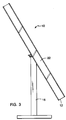
- Fig. 1 is a frontal view of our photovoltaic array.
- Fig. 2 is a rear view of the photovoltaic array of Fig. 1.
- Fig. 3 is a side view of the photovoltaic array of Fig. 1.
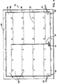
- Fig. 4 is a drawing of a circuit board designed for use in our photovoltaic array.
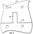
- Fig. 5 is a detailed drawing of a portion of the circuit board of Fig. 4.
- Fig. 6 is a drawing of a solar cell and a secondary optical element mounted on a portion of the circuit board.
- Fig. 7 is a drawing, partially in section, showing a lens focusing solar radiation onto a solar cell.
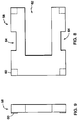
- Fig. 8 is a drawing of a cell placement fixture designed for use in mounting a solar cell onto a circuit board.
- Fig. 9 is a side view of the cell placement fixture of Fig. 8.
- Fig. 10 is a drawing showing a partially cut-away view of a portion of the front surface of our photovoltaic array.
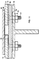
- Fig. 11 is a sectional view of a portion of a photovoltaic array, taken along line 11-11 in Fig. 1.
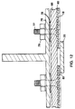
- Fig. 12 is a sectional view of a portion of our photovoltaic array, taken along line 12-12 in Fig. 2.
- Fig. 13 is a sectional view of a portion of a photovoltaic array, taken along line 13-13 in Fig. 1.
- photovoltaic array 10 which may be combined with a large number of similar photovoltaic arrays to form a power plant, consists of a single enclosure 12 having dimensions of 12.954m by 8.9916m by 0.508m (421 ⁇ 2 feet by 291 ⁇ 2 feet by 20 inches).
- Enclosure 12 is supported by an internal unitary structural grid (shown in Figs. 11-13), which is in turn supported by vertical pedestal post 16.
- Pedestal post 16 interfaces with the internal structural grid through a drive mechanism 15 that positions the internal structural grid of the array so that lens parquets 14 face the sun.
- the single-enclosure design minimizes the number of parts and amount of materials needed to enclose the solar cells and the electrical circuitry inside photovoltaic array 10.
- the front face of enclosure 12 includes 120 lens parquets 14 (eleven rows by eleven columns of lens parquets, minus one lens parquet at the location at which vertical pedestal post connects with enclosure 12), each of which includes 24 Fresnel lenses (four rows by six columns) that focus solar radiation onto respective solar cells located within enclosure 12.
- the rear face of enclosure 12 includes 120 circuit board plates 18 on which the solar cells are mounted and to which the solar cells are electrically connected. Trim battens 20 are provided on the front and rear faces of enclosure 12 over the edge regions of lens parquets 14 and circuit board plates 18.
- the side surfaces of enclosure 12 are constructed of sheet metal siding 22. The components located within enclosure 12 are constructed so as not to ignite upon being exposed to concentrated solar radiation.
- the "integrated" photovoltaic array design shown in Figs. 1-3 utilizes a minimal amount of hardware. Another advantage of this design is the ease with which the parts of the array can be shipped for on-site assembly. For example, circuit board plates 18 can be stacked one on top of another in a truck until the truck reaches its weight limit. There is no need to ship large module boxes that weigh little but occupy much space.
- each circuit board plate 18 is 1.16205m (45.75 inches) long and 0.80645m (31.75 inches) wide and has a copper top layer 24 and an aluminum rear layer separated by an electrically insulative layer (as shown in Fig. 7) formed of fiberglass impregnated with epoxy.
- Copper top layer 24 provides electrical circuit paths to which the solar cells are connected, while the thermally conductive aluminum rear layer acts as a heat sink surface, the fiberglass-epoxy electrically insulative layer electrically insulating top layer 24 from the rear layer.
- Top layer 24 includes an etch line 26 that is 0.254 cm (0.100 inches) wide, plus or minus 0.00508 cm (0.002 inches), the centre line of which is 6.6548 cm (2.62 inches) from each of the edges of circuit board plate 18.
- Etch line 26 creates an interruption in top layer 24 (a depression through top layer 24 down to the electrically insulative layer) that electrically isolates the internal portions of top layer 24 from edge region 28.
- Edge region 28 includes twenty 0.4826cm (0.190-inch) screw holes 30 spaced apart every 17.78 cm (seven inches) and centred 4.3688cm (1.72 inches) from the top of etch line 26, which are used for mounting circuit board plate 18 to a gasket located underneath circuit board plate 18 (as shown in Fig. 13).
- Edge region 28 also includes weep holes 82, 0.9525cm (3 ⁇ 8 inch) in diameter, drilled through the circuit board plate, which provide outlets for water that accumulates within the array enclosure due to leakage or condensation. Although drill holes 30 and weep holes 82 create a short circuit between edge region 28 and the aluminum rear layer of circuit board plate 18, edge region 28 is electrically isolated from the internal portions of top layer 24 that function as electrical circuit paths.
- etch lines 32 and 34 divide the internal portions of top layer 24 into copper circuit-path strips 36.
- etch lines 32 and 34 create interruptions in top layer 24 (depressions through top layer 24 down to the electrically insulative layer) that electrically isolate adjacent circuit-path strips 36 so that adjacent circuit-path strips 36 can serve as positive and negative conductors with respect to solar cells that span across a longitudinal etch line 32 and that are secured in electrical (and heat conductive) relationship to the two adjacent circuit-path strips 36 separated by the longitudinal etch line 32.
- Longitudinal etch lines 32 are 0.07112 cm (0.028 inches) wide, plus or minus 0.00508cm (0.002 inches), and transverse etch line 34 is 0.254 cm (0.100 inches) wide, plus or minus 0.00508cm (0.002 inches).
- Bypass diode 27, which is connected betweeen the first and last circuit-path strips 36, bypasses the circuit board in the event of a failure of one or more solar cells, in order to prevent damage to the remaining solar cells.
- a detail of a portion of circuit board plate 18 in the vicinity of a longitudinal etch line 32 includes a portion that surrounds a tooth-shaped region 34 that is 0.4953cm (0.195 inches) wide and 1.18618 cm (0.467 inches) long and over which a solar cell is located (as shown in Fig. 6).
- Each set of four square depressions 37 in the copper top layer of circuit board plate 18, 0.254 cm (0.100 inch) by 0.254 cm (0.100 inch), are used to hold the legs of a cell placement fixture (shown in Figs. 7 and 8) that is used during soldering of the solar cell to circuit board 18.
- Two square depressions each are centred 1.0033cm (0.395 inches) to the left and 1.0033cm (0.395 inches) to the right of the centre line of tooth-shaped region 34.
- the two bottom square depressions are centred 0.58928cm (0.232 inches) below the bottom of etch line 32, and the two top square depressions are centred 2.286cm (0.900 inches) above the two bottom square depressions.
- Each set of four square depressions 37 is centered around a point that is located at the intersection of a vertical line between two drill holes 30 (Fig. 4) and a horizontal line between two drill holes 30.
- Figs. 6 and 7 both illustrate a square, silicon, back-contact solar cell 38 mounted on a portion of circuit board plate 18, and a four-sided, prismatic reflector or "secondary optical element" 40 mounted on top of solar cell 38.
- Secondary optical element 40 directs, by means of reflection, solar radiation that would otherwise miss the active area of solar cell 38 toward the active area- of solar cell 38, the "active area" of the solar cell being the area that is exposed between the four sides of secondary optical element 40.
- the active area of solar cell 38 has dimensions of 1.265 centimeters by 1.265 centimeters.
- Solar cell 38 puts out approximately 61 ⁇ 4 watts of power, at approximately 91 ⁇ 2 amps and approximately 0.65 volts.
- the entire array which includes 2,880 solar cells, consequently puts out approximately 18,000 watts of power.
- Solar cell 38 has a back surface that includes multiple gold contact sections separated by silicon semi-conductor material. Solar cell 38 is soldered onto circuit board plate 18 directly over tooth-shaped region 34. Tooth-shaped region 34 is electrically connected to one of the gold contact sections of solar cell 38, and the adjacent circuit-path strip on circuit board plate 18 is also electrically connected to at least one other gold contact section of solar cell 38.
- circuit board plate 18 provides a circuit in which solar cells are connected in parallel with each other in sets of three, eight of these sets being connected in series.
- Each circuit board plate is connected in series with another circuit board plate by a strap 25 equivalent to a number 4 wire, the strap being located entirely within the array enclosure to avoid exposure to weather.
- a weak cell has an IV curve (voltage as a function of current) that crosses zero volts at a current that is less than the current at which the IV curve of a strong cell crosses zero volts.
- the IV curve of any cell drops off steeply after crossing through zero volts.
- the strong cell or cells force a positive voltage potential across the weak cell, and the weak cell consequently puts out less current than the strong cell or cells.
- the weak cell puts out less current than the strong cells, the weak cell is nevertheless contributing to power production, rather than detracting from power production by cancelling out the power production of other solar cells.
- the distance between 17.78cm by 17.78cm (seven inch by seven inch) Fresnel lens 52 in lens parquet 14 and solar cell 38 is slightly less than 0.508m (20 inches).
- lens 52 which has a focal length of 0.508m (20 inches), directs a beam 50 of solar radiation toward the active area of solar cell 38 in a manner such that the beam is concentrated down to a pattern on solar cell 38 having dimensions that equal the dimensions of the active area of solar cell 38.
- lens 52 is a Fresnel lens, there is chromatic aberration of the light that comes out of the lens, light of each color having its own focal point. Consequently, the edges of the pattern on solar cell 38 consist of red light only, because red light, which has the longest wavelength in the visible spectrum, has a focal point that is further from lens 52 than light of any other color.
- the inside reflective surfaces of secondary optical element 40 do not reflect any substantial portion of radiation beam 50 unless there is misalignment between lens 52 and solar cell 38 or misalignment between lens 52 and the sun. If there is misalignment, the inside reflective surfaces of secondary optical element 40 reflect all radiation that is incident on the inside reflective surfaces toward the active area of the solar cell.
- the focal point of the solar radiation of that wavelength is located below a plane that passes through solar cell 38 and that is parallel to lens 52. It is beneficial not to have any focal points located above the plane that passes through solar cell 38. If any focal points were located above the solar cell, solar radiation would "cross over" the vertical optical axis at the focal points. It would be necessary to construct the sides of prismatic secondary optical element 40 at a relatively narrow angle with respect to the vertical direction, in order to prevent crossed-over radiation that hits one inside surface of secondary optical element 40 from being reflected toward the inside surface on the opposite side of the secondary optical element, and from the inside surface on the opposite side being reflected out of secondary optical element 40.
- secondary optical element 40 can be constructed with sides that form an angle with respect to the vertical direction that is great enough to permit secondary optical element 40 to be relatively forgiving of misalignment errors between lens 52 and solar cell 38.
- the sides of secondary optical element 40 were constructed at an angle that is too great with respect to the vertical direction the radiation that hits one inside surface of secondary optical element 40 would be reflected toward the inside surface on the opposite side of the secondary optical element, and from the inside surface on the opposite side would be reflected out of the secondary optical element.
- the ratio of concentration of solar radiation incident on solar cell 38 relative to the concentration of the solar radiation before passing through lens 52 is preferably between 150 and 250.
- the ratio of concentration is too high, the photons from the solar radiation, which are supposed to dislodge electrons in the semiconductor material of solar cell 38, begin to saturate the solar cell. Consequently, solar cell 38 yields fewer and fewer electrons per photon, and hence yields less current, as the ratio of concentration increases.
- the peak efficiency of solar cell 38 is achieved at a concentration ratio of approximately 200.
- circuit board plate 18 is a laminate that includes top copper layer 24, having a thickness of approximately 0.00508 cm (0.002 inches), which provides electrical circuit paths to which the solar cells are connected, rear aluminium layer 54, having a thickness of approximately 0.0762cm (0.030 inches), which functions as a heat sink, and internal, electrically insulative layer 56, having a thickness of approximately 0.00762 cm (0.003 inches), which is preferably a layer of fiberglass impregnated with epoxy. Dried fiberglass-epoxy layer 56 is epoxied to copper layer 24 and aluminum iayer 54.
- Fiberglass-epoxy layer 56 has a dielectric strength of approximately 4000 volts, yet the temperature drop across fiberglass-epoxy layer 56 is only approximately 6°C (11 degrees fahrenheit). Note that both the dielectric strength of the fiberqlass-epoxy layer and the temperature drop across the fiberqlass-epoxy layer increase as a function of the thickness of the fiberglass-epoxy layer.
- circuit board plate 18 may be tested by heating the circuit board plate up to 216°C 420 degrees fahrenheit to determine whether the circuit board plate will come apart.
- the photovoltaic array includes the series connection of 960 sets of three solar cells connected in parallel, each set of parallelly connected solar cells producing a voltage that is approximately 0.65 volts higher than the voltage produced by the previous set.
- the photovoltaic array includes the series connection of 1440 sets of two solar cells connected in parallel, in which case voltages as high as 900 volts can be built up inside the photovoltaic array.
- Electrical insulators typically have a low thermal conductivity. Nevertheless, it is important that the temperature drop across electrically insulative layer 56 be as low as possible. Approximately 25 percent of the solar radiation that enters the photovoltaic array is converted into electrical power and the other 75 percent is absorbed by the photovoltaic array as heat. When the temperature of the silicon in a solar cell is raised the voltage across the solar cell drops. Consequently, if fiberglass-epoxy electrically insulative layer 56 were too thick, the solar cells would heat up to a point at which the efficiency of the solar cells would be reduced.
- the top surface of aluminum layer 54 may be black anodized, to create an anodized electrically insulative film that makes up electrically insulative layer 56.
- the anodized electrically insulative film which is epoxied to copper layer 24, has a dielectric strength of approximately 800 volts.
- the epoxy has a thickness of approximately 25.4 micrometers (0.001 inches).
- This alternative method of constructing the circuit board plate can be used in a photovoltaic array in which the solar cells are interconnected in a manner such that the maximum voltage potential across the circuit board plate is 300 volts, e.g., an array that includes the series connection of 480 sets of six solar cells connected in parallel. Recall that when solar cells are connected in series, voltages add, whereas when solar cells are connected in parallel, currents add.
- the solar cell should be positioned on the circuit board plate with an accuracy of plus or minus 127 micrometers (0.005 inches) with respect to all other solar cells.
- aluminium cell placement fixture 58 is used as a physical guide during the soldering process by which the solar cell and the copper tabs are attached to the circuit board plate, to achieve an accuracy in the placement of the solar cell and the copper tabs on the circuit board plate of plus or minus 50.8 micrometers (0.002 inches).
- Cell placement fixture 58 is 2.76352cm (1.088 inches) long by 2.25552cm (0.888 inches) wide by 0.3175cm (0.125 inches) thick (excluding the thickness of legs 60).
- the four legs 60 having dimensions of 0.024892cm (0.098 inches) by 0.24892cm (0.098 inches) by 0.0254cm (0.010 inches), are designed to fit into square depressions 37 in the circuit board plate (Fig. 6).
- the circuit board plate After the soldering foils have been placed on the circuit board plate, but before the solar cell and the copper tabs are in position over the respective soldering foils, the circuit board plate is placed over a hot plate, causing the soldering foils to melt. Flux is then applied to the solar cells and the tabs, the solar cells and tabs are placed on top of the melted solder, and weights are applied on top of the solar cells and tabs. The circuit board plate is then removed from the hot plate to permit cooling of the solder connections, which takes approximately five minutes, and when the solder is hard cell placement fixtures 58 are removed from the circuit board.
- the top surface of the photovoltaic array includes lens parquets 14 having trim battens 20 placed over the edge regions of each lens parquet. Rubber gaskets 66 are located between trim battens 20 and lens parquets 14 for the purpose of preventing water from entering the array enclosure.
- Metal gutter plates 68 having gutter channels 69 are provided beneath trim battens 20, running from the top of the front face of the array to the bottom of the front face of the array, for the purpose of capturing water that does leak through gaskets 66 and channeling the captured water off of the array, thereby preventing the captured water from dripping down onto the cell packages inside the photovoltaic array. Screws 72 attach trim battens 20 to extrusion channels 73 provided in gutter plates 68.
- Metal water shields 70 extend in the horizontal direction, each water shield having a section located beneath one of the lens parquets, a section located above a portion of another of the lens parquets, and a vertical water-interception section located between the two other sections.
- Water shields 70 are constructed to capture water that leaks through the gaskets beneath the trim battens that extend in the horizontal direction (not shown), and to prevent the captured water from entering beneath the second of the lens parquets.
- the captured water is channeled into gutter plates 68 located to the left and to the right of each water shield 70. Rubber gaskets 74 are located between lens parquets 14 and both water shields 70 and gutter plates 68.
- gutter plate 68 is bolted to internal structural grid member 76 (which forms part of the internal structural grid shown in more detail in Fig. 13) by bolts 77 and nuts 79.
- Leveling shims 78 are provided between gutter plate 68 and structural grid member 76. By loosening nuts 79 it is possible to remove or add leveling shims 78 between structural grid member 76 and gutter plate 68 to compensate for any warping or sagging of the internal structural grid, thereby enhancing the degree of flatness of the top surface of the array enclosure so that each of lens parquets 14 can directly face the sun.
- Leveling shims 78 are provided at each of the corners of each lens .parquet 14, as well as approximately every 35.56cm (14 inches) along the sides of each lens parquet 14 (at two locations along each of the longer sides of each lens parquet and at one location at the center of each of the shorter sides).
- lens parquets 14 are positioned on top of the structural grid and secured on top of gutter plate 68 by trim battens 20.
- Gasket 66 is located between trim batten 20 and lens parquets 14, and gasket 74 is located between lens parquets 14 and gutter plate 68.
- Water shield 70 has one section located beneath one of lens parquets 14, another section located above a portion of another of lens parquets 14, and a vertical water-interception section located between the two other sections.
- Fig. 12 shows a sectional view of a portion of the bottom of the photovoltaic array as taken along line 12-12 in Fig. 2, structural grid member 76 is bolted to inverted gutter plate 68, which serves no water-channeling function but is used for the sake of symmetric design simplicity.
- Leveling shims 78 are provided between gutter plate 68 and structural grid member 76.
- Trim batten 20 secures circuit board plates 18 below gutter plate 68.
- Gasket 80 is located between circuit board plates 18 and gutter plate 68.
- One or more weep holes 82 0.9525cm (5 ⁇ 8 inch) in diameter, are provided in each of circuit board plates 18 to provide outlets for water that is present inside the array enclosure due to leakage or condensation.
- Weep holes 82 are drilled through circuit board plate 18 at locations (shown in Fig. 4) above which gasket 80 and gutter plate 68 are not present.
- the internal structural grid includes longitudinal structural grid members 76 (also shown in Figs. 11 and 12), transverse structural grid members 88, and vertical structural grid members 90.
- Each rectangular region of the photovoltaic array is bounded by four transverse structural grid members 88, four longitudinal structural grid members 76 (two of which are shown), and four vertical structural grid members 90 (two of which are shown).
- the internal structural grid also includes member 84, which extends lengthwise across the middle of the rectangular region of the photovoltaic array. Structural grid member 84, unlike the other structural grid members, passes directly over the electrically alive regions of circuit board plate 18. The bottom of structural grid member 84 is spaced apart from circuit board plate 18. Member piece 84 is clamped to two solid aluminum rods 86 that extend upwards toward lens parquet 14, to which aluminum rods 86 are epoxied. Aluminum rods 86 support lens parquet 14 at two locations separated apart by approximately 35.56cm (14 inches), each location being equidistant (14 inches - 35.56cm) from three of the edges of lens parquet 14.
- Fig. 13 Also shown in Fig. 13 are No. 10 screws 92, which fit through screw holes 30 (Fig. 4) in circuit board plate 18. Screws 92 connect circuit board plate 18 to gasket 80. Note that the trim battens 20 that are located on the corners between the top surface of the enclosure and sheet metal side surface 22 and the corners between the bottom surface of the enclosure and sheet metal side surface 22 wrap around the corner to clamp the sheet metal in place so that wind forces will not blow the sheet metal off of the photovoltaic array.
- the internal structural grid is of a type that does not include a torque tube extending in the horizontal direction. Such a torque tube can occupy a substantial amount of space. Consequently, it is possible to provide lens parquets across the entire front surface of the photovoltaic array and to distribute solar cells uniformly throughout the entire inside of the photovoltaic array, except at the single location at which the pedestal attaches to the structural grid.
Landscapes
- Engineering & Computer Science (AREA)
- Physics & Mathematics (AREA)
- Life Sciences & Earth Sciences (AREA)
- Sustainable Development (AREA)
- Sustainable Energy (AREA)
- Thermal Sciences (AREA)
- Chemical & Material Sciences (AREA)
- Combustion & Propulsion (AREA)
- Mechanical Engineering (AREA)
- General Engineering & Computer Science (AREA)
- Photovoltaic Devices (AREA)
- Charge And Discharge Circuits For Batteries Or The Like (AREA)
Applications Claiming Priority (3)
| Application Number | Priority Date | Filing Date | Title |
|---|---|---|---|
| US07/690,194 US5125983A (en) | 1991-04-22 | 1991-04-22 | Generating electric power from solar radiation |
| PCT/US1992/003067 WO1992019016A1 (en) | 1991-04-22 | 1992-04-14 | Generating electric power from solar radiation |
| US690194 | 1996-07-26 |
Publications (3)
| Publication Number | Publication Date |
|---|---|
| EP0581889A1 EP0581889A1 (en) | 1994-02-09 |
| EP0581889A4 EP0581889A4 (OSRAM) | 1994-05-04 |
| EP0581889B1 true EP0581889B1 (en) | 1997-03-26 |
Family
ID=24771496
Family Applications (1)
| Application Number | Title | Priority Date | Filing Date |
|---|---|---|---|
| EP92912817A Expired - Lifetime EP0581889B1 (en) | 1991-04-22 | 1992-04-14 | Generating electric power from solar radiation |
Country Status (9)
| Country | Link |
|---|---|
| US (1) | US5125983A (OSRAM) |
| EP (1) | EP0581889B1 (OSRAM) |
| CN (1) | CN1031159C (OSRAM) |
| AU (1) | AU655300B2 (OSRAM) |
| ES (1) | ES2101102T3 (OSRAM) |
| GR (1) | GR3023433T3 (OSRAM) |
| IL (1) | IL101521A (OSRAM) |
| TW (1) | TW231375B (OSRAM) |
| WO (1) | WO1992019016A1 (OSRAM) |
Families Citing this family (53)
| Publication number | Priority date | Publication date | Assignee | Title |
|---|---|---|---|---|
| CN1035912C (zh) * | 1993-11-06 | 1997-09-17 | 杨永清 | 光电供电设备 |
| JPH07202242A (ja) * | 1993-11-26 | 1995-08-04 | Sanyo Electric Co Ltd | 太陽電池モジュール及び太陽電池装置 |
| US5460659A (en) * | 1993-12-10 | 1995-10-24 | Spectrolab, Inc. | Concentrating photovoltaic module and fabrication method |
| US5498297A (en) * | 1994-09-15 | 1996-03-12 | Entech, Inc. | Photovoltaic receiver |
| US20100108118A1 (en) * | 2008-06-02 | 2010-05-06 | Daniel Luch | Photovoltaic power farm structure and installation |
| US20090293941A1 (en) * | 2008-06-02 | 2009-12-03 | Daniel Luch | Photovoltaic power farm structure and installation |
| US8664030B2 (en) | 1999-03-30 | 2014-03-04 | Daniel Luch | Collector grid and interconnect structures for photovoltaic arrays and modules |
| US6248949B1 (en) * | 1999-10-28 | 2001-06-19 | Gerald A. Turner | Method of manufacturing a solar cell receiver plate of a concentrator photovoltaic array |
| JP4270689B2 (ja) * | 1999-11-24 | 2009-06-03 | 本田技研工業株式会社 | 太陽光発電装置 |
| US6294725B1 (en) * | 2000-03-31 | 2001-09-25 | Trw Inc. | Wireless solar cell array electrical interconnection scheme |
| US6498290B1 (en) * | 2001-05-29 | 2002-12-24 | The Sun Trust, L.L.C. | Conversion of solar energy |
| US6559371B2 (en) * | 2001-06-27 | 2003-05-06 | Pinnacle West Capital Corp. | High-concentration photovoltaic assembly for a utility-scale power generation system |
| US6531653B1 (en) * | 2001-09-11 | 2003-03-11 | The Boeing Company | Low cost high solar flux photovoltaic concentrator receiver |
| ATE356440T1 (de) * | 2002-05-17 | 2007-03-15 | Jason E Schripsema | Photovoltaisches modul mit einstellbarem kühlkörper und herstellungsverfahren |
| US7190531B2 (en) * | 2003-06-03 | 2007-03-13 | Rensselaer Polytechnic Institute | Concentrating type solar collection and daylighting system within glazed building envelopes |
| US7759158B2 (en) * | 2005-03-22 | 2010-07-20 | Applied Materials, Inc. | Scalable photovoltaic cell and solar panel manufacturing with improved wiring |
| HU3056U (en) | 2005-04-29 | 2006-03-28 | G & G Noevenyvedelmi Es Keresk | Construction for making weed map |
| US8026440B1 (en) | 2005-09-07 | 2011-09-27 | Amonix, Inc. | Passively cooled, high concentration photovoltaic solar cell package |
| US8884155B2 (en) | 2006-04-13 | 2014-11-11 | Daniel Luch | Collector grid and interconnect structures for photovoltaic arrays and modules |
| US9236512B2 (en) | 2006-04-13 | 2016-01-12 | Daniel Luch | Collector grid and interconnect structures for photovoltaic arrays and modules |
| US8822810B2 (en) | 2006-04-13 | 2014-09-02 | Daniel Luch | Collector grid and interconnect structures for photovoltaic arrays and modules |
| US9006563B2 (en) | 2006-04-13 | 2015-04-14 | Solannex, Inc. | Collector grid and interconnect structures for photovoltaic arrays and modules |
| US8729385B2 (en) | 2006-04-13 | 2014-05-20 | Daniel Luch | Collector grid and interconnect structures for photovoltaic arrays and modules |
| US9865758B2 (en) | 2006-04-13 | 2018-01-09 | Daniel Luch | Collector grid and interconnect structures for photovoltaic arrays and modules |
| US7999174B2 (en) * | 2006-10-09 | 2011-08-16 | Solexel, Inc. | Solar module structures and assembly methods for three-dimensional thin-film solar cells |
| US8084684B2 (en) | 2006-10-09 | 2011-12-27 | Solexel, Inc. | Three-dimensional thin-film solar cells |
| US7728219B2 (en) * | 2006-12-11 | 2010-06-01 | Sunmodular, Inc. | Photovoltaic cells, modules and methods of making same |
| US20080134497A1 (en) * | 2006-12-11 | 2008-06-12 | Sunmodular, Inc. | Modular solar panels with heat exchange & methods of making thereof |
| US20080135088A1 (en) * | 2006-12-11 | 2008-06-12 | Sunmodular, Inc. | Interlocking solar roof tiles with heat exchange |
| US8609978B2 (en) * | 2007-02-14 | 2013-12-17 | Flextronics Ap, Llc | Leadframe based photo voltaic electronic assembly |
| US20080271774A1 (en) * | 2007-05-01 | 2008-11-06 | Kalkanoglu Husnu M | Photovoltaic Roofing Wiring Array, Photovoltaic Roofing Wiring System and Roofs Using Them |
| US20090159125A1 (en) * | 2007-12-21 | 2009-06-25 | Eric Prather | Solar cell package for solar concentrator |
| US20100108140A1 (en) * | 2008-03-14 | 2010-05-06 | E. I. Du Pont De Nemours And Company | Device capable of thermally cooling while electrically insulating |
| US20090255566A1 (en) * | 2008-04-14 | 2009-10-15 | Visera Technologies Company Limited | Solar cell modules |
| US8697553B2 (en) * | 2008-06-11 | 2014-04-15 | Intevac, Inc | Solar cell fabrication with faceting and ion implantation |
| KR20100073084A (ko) * | 2008-12-22 | 2010-07-01 | 삼성전자주식회사 | 태양광열 이용장치 및 그 조립방법 |
| CN102388464B (zh) * | 2009-02-09 | 2016-09-07 | 森普留斯公司 | 集中器型光电(cpv)模块、接收器和子接收器及其形成方法 |
| US20100200045A1 (en) * | 2009-02-09 | 2010-08-12 | Mitchell Kim W | Solar power system and method of manufacturing and deployment |
| US8749053B2 (en) | 2009-06-23 | 2014-06-10 | Intevac, Inc. | Plasma grid implant system for use in solar cell fabrications |
| US20100326492A1 (en) * | 2009-06-30 | 2010-12-30 | Solarmation, Inc. | Photovoltaic Cell Support Structure Assembly |
| CN101882633A (zh) * | 2010-07-14 | 2010-11-10 | 西安交通大学 | 带有自聚焦透镜层的太阳能电池 |
| CN101937937B (zh) * | 2010-08-27 | 2012-06-27 | 成都钟顺科技发展有限公司 | 复眼式聚光太阳电池组件及其制造工艺 |
| JP6090694B2 (ja) | 2010-10-27 | 2017-03-08 | 株式会社クラレ | 光発電装置 |
| US9893223B2 (en) | 2010-11-16 | 2018-02-13 | Suncore Photovoltaics, Inc. | Solar electricity generation system |
| TWI506719B (zh) | 2011-11-08 | 2015-11-01 | 因特瓦克公司 | 基板處理系統及方法 |
| US20130213473A1 (en) * | 2012-02-21 | 2013-08-22 | Atomic Energy Council - Institute Of Nuclear Energy Research | Composite substrate with high thermal conductivity |
| WO2014037757A1 (en) * | 2012-09-07 | 2014-03-13 | Doci Innovations GmbH | Concentrator system for converting light into electrical energy |
| MY178951A (en) | 2012-12-19 | 2020-10-23 | Intevac Inc | Grid for plasma ion implant |
| JP5977686B2 (ja) | 2013-02-13 | 2016-08-24 | 信越化学工業株式会社 | 集光型太陽電池モジュールの製造方法及び集光型太陽電池モジュール |
| US20150162871A1 (en) * | 2013-12-06 | 2015-06-11 | Jean-Claude Koffi Rock | Method of Cell Isolation in Photovoltaic Solar Module or Solar Array |
| CN104176373A (zh) * | 2014-08-01 | 2014-12-03 | 湖南红太阳新能源科技有限公司 | 一种柔性薄膜材料的支撑架 |
| US10418501B2 (en) | 2015-10-02 | 2019-09-17 | X-Celeprint Limited | Wafer-integrated, ultra-low profile concentrated photovoltaics (CPV) for space applications |
| US10615744B2 (en) * | 2017-08-13 | 2020-04-07 | The Aerospace Corporation | Intelligent solar cell carrier system for flight and laboratory measurement applications |
Family Cites Families (13)
| Publication number | Priority date | Publication date | Assignee | Title |
|---|---|---|---|---|
| US3574725A (en) | 1966-08-11 | 1971-04-13 | Sankyo Chem Ind Ltd | Method for preparing l-(-)-alpha-methyl-beta-(3,4-dihydroxyphenyl)-alanine |
| FR1593348A (OSRAM) * | 1967-12-07 | 1970-05-25 | ||
| US3849880A (en) * | 1969-12-12 | 1974-11-26 | Communications Satellite Corp | Solar cell array |
| FR2465315A1 (fr) * | 1979-09-10 | 1981-03-20 | Radiotechnique Compelec | Panneau generateur photovoltaique assurant l'etancheite aux intemperies d'une toiture par pose directe sur la charpente |
| US4357400A (en) * | 1979-12-11 | 1982-11-02 | Electric Power Research Institute, Inc. | Photoelectrochemical cell employing discrete semiconductor bodies |
| US4454372A (en) * | 1981-04-17 | 1984-06-12 | Electric Power Research Institute, Inc. | Photovoltaic battery |
| US4836861A (en) * | 1987-04-24 | 1989-06-06 | Tactical Fabs, Inc. | Solar cell and cell mount |
| US4865999A (en) * | 1987-07-08 | 1989-09-12 | Glasstech Solar, Inc. | Solar cell fabrication method |
| US4927770A (en) * | 1988-11-14 | 1990-05-22 | Electric Power Research Inst. Corp. Of District Of Columbia | Method of fabricating back surface point contact solar cells |
| US4933022A (en) * | 1988-11-14 | 1990-06-12 | Board Of Trustees Of The Leland Stanford Univ. & Electric Power Research Institute | Solar cell having interdigitated contacts and internal bypass diodes |
| US4933021A (en) * | 1988-11-14 | 1990-06-12 | Electric Power Research Institute | Monolithic series-connected solar cells employing shorted p-n junctions for electrical isolation |
| US4968355A (en) * | 1989-04-14 | 1990-11-06 | Johnson Kenneth C | Two-axis tracking solar collector mechanism |
| US5176758A (en) * | 1991-05-20 | 1993-01-05 | United Solar Systems Corporation | Translucent photovoltaic sheet material and panels |
-
1991
- 1991-04-22 US US07/690,194 patent/US5125983A/en not_active Expired - Lifetime
-
1992
- 1992-04-07 IL IL10152192A patent/IL101521A/en unknown
- 1992-04-10 TW TW081102809A patent/TW231375B/zh active
- 1992-04-14 EP EP92912817A patent/EP0581889B1/en not_active Expired - Lifetime
- 1992-04-14 AU AU21677/92A patent/AU655300B2/en not_active Ceased
- 1992-04-14 ES ES92912817T patent/ES2101102T3/es not_active Expired - Lifetime
- 1992-04-14 WO PCT/US1992/003067 patent/WO1992019016A1/en not_active Ceased
- 1992-04-21 CN CN92103129A patent/CN1031159C/zh not_active Expired - Fee Related
-
1997
- 1997-05-15 GR GR970401082T patent/GR3023433T3/el unknown
Also Published As
| Publication number | Publication date |
|---|---|
| TW231375B (OSRAM) | 1994-10-01 |
| CN1066150A (zh) | 1992-11-11 |
| CN1031159C (zh) | 1996-02-28 |
| AU655300B2 (en) | 1994-12-15 |
| AU2167792A (en) | 1992-11-17 |
| WO1992019016A1 (en) | 1992-10-29 |
| US5125983A (en) | 1992-06-30 |
| IL101521A (en) | 1994-06-24 |
| GR3023433T3 (en) | 1997-08-29 |
| IL101521A0 (en) | 1992-12-30 |
| ES2101102T3 (es) | 1997-07-01 |
| EP0581889A1 (en) | 1994-02-09 |
| EP0581889A4 (OSRAM) | 1994-05-04 |
Similar Documents
| Publication | Publication Date | Title |
|---|---|---|
| EP0581889B1 (en) | Generating electric power from solar radiation | |
| US20080185034A1 (en) | Fly's Eye Lens Short Focal Length Solar Concentrator | |
| EP0535614B1 (en) | Solar battery module | |
| US11594651B2 (en) | Cell module | |
| JP2008543066A (ja) | 光起電集光装置及び前記から形成された光起電集光モジュール並びにこれらのための生産方法 | |
| US20090183762A1 (en) | Low-voltage tracking solar concentrator | |
| US8586858B2 (en) | Passively cooled, high concentration photovoltaic solar cell package | |
| BRMU9100775U2 (pt) | màdulo de sistema fotovoltÁico concentrado usando cÉlulas solares de semicondutor iii - v | |
| KR20120018369A (ko) | 광전도 모듈 스트링 배열 및 그 쉐이딩 보호 | |
| US20100288332A1 (en) | Solar photovoltaic concentrator panel | |
| US11600733B2 (en) | System and method for shingling wafer strips connected in parallel | |
| KR100922887B1 (ko) | 광집속형 태양전지 모듈 | |
| US20110203638A1 (en) | Concentrating linear photovoltaic receiver and method for manufacturing same | |
| Hayashi et al. | Nonuniformity sunlight-irradiation effect on photovoltaic performance of concentrating photovoltaic using microsolar cells without secondary optics | |
| CN222190760U (zh) | 一种背接触电池组件和光伏发电系统 | |
| RU2690728C1 (ru) | Концентраторно-планарный солнечный фотоэлектрический модуль | |
| JP2013207079A (ja) | 集光型太陽光発電パネル及び集光型太陽光発電装置 | |
| JP6292266B2 (ja) | 集光型太陽光発電パネル及び集光型太陽光発電装置 | |
| CN101208806A (zh) | 光伏聚光器与其形成的聚光太阳电池组件及其制造方法 | |
| RU2475888C1 (ru) | Конструкция фотоэлектрического модуля | |
| CN223666693U (zh) | 一种太阳能电池串及太阳能电池组件 | |
| CN223472503U (zh) | 一种太阳能电池、太阳能电池组件及光伏系统 | |
| CN223488658U (zh) | 太阳能电池组件及光伏系统 | |
| Yu et al. | High‐Efficiency Multi‐Cell TPV Module Fabrication and Performance | |
| CN120658197A (zh) | 聚光光伏模组 |
Legal Events
| Date | Code | Title | Description |
|---|---|---|---|
| PUAI | Public reference made under article 153(3) epc to a published international application that has entered the european phase |
Free format text: ORIGINAL CODE: 0009012 |
|
| 17P | Request for examination filed |
Effective date: 19931119 |
|
| AK | Designated contracting states |
Kind code of ref document: A1 Designated state(s): ES GR IT |
|
| A4 | Supplementary search report drawn up and despatched |
Effective date: 19940315 |
|
| AK | Designated contracting states |
Kind code of ref document: A4 Designated state(s): ES GR IT |
|
| 17Q | First examination report despatched |
Effective date: 19950202 |
|
| GRAG | Despatch of communication of intention to grant |
Free format text: ORIGINAL CODE: EPIDOS AGRA |
|
| GRAH | Despatch of communication of intention to grant a patent |
Free format text: ORIGINAL CODE: EPIDOS IGRA |
|
| GRAH | Despatch of communication of intention to grant a patent |
Free format text: ORIGINAL CODE: EPIDOS IGRA |
|
| GRAA | (expected) grant |
Free format text: ORIGINAL CODE: 0009210 |
|
| AK | Designated contracting states |
Kind code of ref document: B1 Designated state(s): ES GR IT |
|
| ITF | It: translation for a ep patent filed | ||
| REG | Reference to a national code |
Ref country code: ES Ref legal event code: FG2A Ref document number: 2101102 Country of ref document: ES Kind code of ref document: T3 |
|
| REG | Reference to a national code |
Ref country code: GR Ref legal event code: FG4A Free format text: 3023433 |
|
| PLBE | No opposition filed within time limit |
Free format text: ORIGINAL CODE: 0009261 |
|
| STAA | Information on the status of an ep patent application or granted ep patent |
Free format text: STATUS: NO OPPOSITION FILED WITHIN TIME LIMIT |
|
| 26N | No opposition filed | ||
| PGFP | Annual fee paid to national office [announced via postgrant information from national office to epo] |
Ref country code: ES Payment date: 19980629 Year of fee payment: 7 |
|
| PGFP | Annual fee paid to national office [announced via postgrant information from national office to epo] |
Ref country code: GR Payment date: 19980630 Year of fee payment: 7 |
|
| PG25 | Lapsed in a contracting state [announced via postgrant information from national office to epo] |
Ref country code: ES Free format text: LAPSE BECAUSE OF NON-PAYMENT OF DUE FEES Effective date: 19990415 |
|
| PG25 | Lapsed in a contracting state [announced via postgrant information from national office to epo] |
Ref country code: GR Free format text: LAPSE BECAUSE OF NON-PAYMENT OF DUE FEES Effective date: 19990430 |
|
| REG | Reference to a national code |
Ref country code: ES Ref legal event code: FD2A Effective date: 20010503 |
|
| PG25 | Lapsed in a contracting state [announced via postgrant information from national office to epo] |
Ref country code: IT Free format text: LAPSE BECAUSE OF NON-PAYMENT OF DUE FEES Effective date: 20050414 |