EP0571015A1 - Elektrolytisches Reinigungsverfahren für Metalloberfläche von elektronischen Bauelementen - Google Patents
Elektrolytisches Reinigungsverfahren für Metalloberfläche von elektronischen Bauelementen Download PDFInfo
- Publication number
- EP0571015A1 EP0571015A1 EP93201321A EP93201321A EP0571015A1 EP 0571015 A1 EP0571015 A1 EP 0571015A1 EP 93201321 A EP93201321 A EP 93201321A EP 93201321 A EP93201321 A EP 93201321A EP 0571015 A1 EP0571015 A1 EP 0571015A1
- Authority
- EP
- European Patent Office
- Prior art keywords
- solution
- bleed
- plastic
- lactate
- added
- Prior art date
- Legal status (The legal status is an assumption and is not a legal conclusion. Google has not performed a legal analysis and makes no representation as to the accuracy of the status listed.)
- Granted
Links
Images
Classifications
-
- H—ELECTRICITY
- H10—SEMICONDUCTOR DEVICES; ELECTRIC SOLID-STATE DEVICES NOT OTHERWISE PROVIDED FOR
- H10W—GENERIC PACKAGES, INTERCONNECTIONS, CONNECTORS OR OTHER CONSTRUCTIONAL DETAILS OF DEVICES COVERED BY CLASS H10
- H10W70/00—Package substrates; Interposers; Redistribution layers [RDL]
- H10W70/01—Manufacture or treatment
- H10W70/05—Manufacture or treatment of insulating or insulated package substrates, or of interposers, or of redistribution layers
- H10W70/097—Cleaning
-
- C—CHEMISTRY; METALLURGY
- C25—ELECTROLYTIC OR ELECTROPHORETIC PROCESSES; APPARATUS THEREFOR
- C25F—PROCESSES FOR THE ELECTROLYTIC REMOVAL OF MATERIALS FROM OBJECTS; APPARATUS THEREFOR
- C25F1/00—Electrolytic cleaning, degreasing, pickling or descaling
Definitions
- the invention relates to a method for the electrolytic removal of plastic flash or bleed from the metal surfaces of semiconductor devices and similar electronic components by immersing such components in a water based solution of one or more organic solvents, conducting salts and a wetting agent and connecting the components to be cleaned to the negative pole of a source of direct current of which the positive pole is connected to a counter electrode in the same solution.
- the invention also relates to the composition of the solution to be used for immersing the components.
- a carrier called a leadframe is stamped or etched from a copper alloy, nickel-iron alloy or another metal.
- a leadframe comprises generally a pad and a number of leads.
- the central part of the leadframe consisting of pad and leadtips is subsequently selectively electroplated with metals such as gold, silver, palladium, copper or nickel.
- metals such as gold, silver, palladium, copper or nickel.
- a chip is bonded to the leadframe pad and electric wire connections are made between chip and leadtips (wirebonding), followed bij encapsulating the central area containing the chip and wirebonded leadtips by injection molding with a plastic, usually an epoxy based plastic.
- a plastic usually an epoxy based plastic.
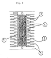
- the plastic encapsulation which contains the bonded chip and the wirebonded leadtips is indicated with numeral 1, the outer leads with 2.
- Numeral 3 indicates spaces which usually fill up with plastic during molding of encapsulation 1, whilst numeral 4 indicates places where very thin films of plastic (normally called “bleed”) can contaminate the metal surface of the outer leads and which must be removed.
- Numeral 5 indicates parts of the leadframe serving interconnection during manufacturing and which will be removed before the IC is used.
- the method of this invention is designed to remove the plastic bleed as indicated in the drawing with numeral 4.
- plastic bleed films on the metal surface of the leads are thin, usually less than 10 micrometer, but must be carefully removed to avoid uncoated areas during subsequent tin-lead plating, necessary to enable reliable solder connections to be made to other parts of an electronic circuit.
- the traditional way to remove the plastic bleed films from the molded components is to submit the components to abrasive blasting with ground cherry or apricot stones, fine, relatively hard plastic grains or glass beads and the like.
- the blasting operations is preceded by softening of the plastic bleed in organic solvents or by extended treatment in diluted warm acids.
- a disadvantage of blasting with fine particles is that some of these particles will be embedded in the metal surface of the leads and must be carefully removed before plating with a solderable coating and that the blasting operation will create roughness of the metal surface.
- US Patent 4,968,397 describes an electrolytic anodic process with which embedded blasting particles can be removed, whilst simultaneously metal bleed, such as silver, extending on the leads outside the plastic encapsulation is dissolved, resulting in a clean surface of the leads.
- metal bleed such as silver
- US Patent 4,781,804 describes a method to remove plastic bleed from the leads of semiconductor components by means of an electrolytic treatment in a solution containing an alkali metal hydroxide, detergent, a glycol compound, alkali-metal bicarbonate, ethoxylated furfuryl alcohol, tetrahydro furfuryl alcohol and a fluorinated surfactant in water and whereby the components are connected as a cathode to a source of direct current so that hydrogen is generated on the metal surface upon current passages.
- this solution contains aggressive components attacking the material of the plastic encapsulation.
- an improved method is obtained for removing plastic bleed from outer leads of encapsulated semiconductor components whereby the encapsulating material is not attacked and whereby no additional surface treatments are necessary before subsequent solderplating.
- the metal surface was frequently necessary to subject the metal surface to a chemical or electrolytic polishing treatment after plastic bleed removal.
- this method is characterised in that, during passage of a current through the solution, the pH of the liquid film directly adjacent to the cathodic metallic surface is raised to a value at which the solvent in the solution causes a softening action on the plastic bleed, which is sufficient to enable the hydrogen gas generated simultaneously on the cathode to remove the plastic mold flash or bleed from the metal surface.
- the solvents present in the electrolyte, supported by the wetting agent soften the plastic bleed to such an extend that the hydrogen gas generated at the metal surface simultaneously is able to mechanically scrub the surface clean of the softened plastic bleed.
- esters of lactic acid are added to the water based solution.
- Preferred esters are methyl, ethyl, isopropyl or butyl lactate.
- the alkyl esters with the lower number of carbon atoms are best soluble in water.
- the water based solution contains 10 - 20% by volume alkyl lactate.
- Salts which must be added to obtain sufficient conductivity of the solution can be organic or inorganic but are preferably potassium, sodium or ammonium salts of acetic or lactic acid, whilst suitable inorganic salts are the potassium, sodium and ammonium salts of sulphuric, phosphoric or carbonic acids. Chlorides would also be suitable but are usually not permitted in the manufacturing process of semiconductors.
- the concentration of conducting salts must be adequate to provide a pH between 10 - 13 in the catholyte when a direct current is applied with a cathodic current density of 25 - 40 A/dm2 and at which the pH of the bulk of the electrolyte is maintained between 6 and 7.
- lactates are used as conducting salts to reduce the number of ions in the solution and to reduce the hydrolyses of the alkyl lactate.
- the softening effect of alkyl esters of lactic acid on plastic bleed could be further improved by the addition of other water soluble solvents, particularly by addition of 0.5 - 2.5 ml/liter 4-methyl-2-pentanol.
- the method of the present invention utilises this phenomena for removal of plastic bleed from metal surfaces by employing a solution with a pH between 6.5 and 7.5. At this pH, hydrolysis of alkyl lactates is negligeable. When direct current is passed through the solution at which the components are cathodic and the C.D. has a value between 30 - 40 A/dm2 the pH in the catholyte will increase to a value well over 12. These high pH values are created only in the areas where metal is exposed, such as in the pores of the plastic bleed and the immediate area surrounding the pores. There will be no pH increase at the surface of the bulk of plastic encapsulating material.
- the method for removing plastic bleed from metal surfaces utilises a solution with a temperature between 35 and 50 °C, preferably at appr. 45 °C for appr. 1 minute. Even after longer exposure times no attack of plastic encapsulating material will take place, in areas other than the plastic bleed film which must be removed.
- Leadframes for integrated circuits were manufactured and assembled in the standard industrial way, and finally encapsulated with an epoxy based plastic. These leadframes showed plastic bleed on the outer lead metal surfaces. This plastic bleed film was removed using the method of this invention as will be explained hereafter. The process time for removing the plastic bleed was 1 minute and 15 seconds and followed by a pressurised water rinse during 5 seconds, after which a final treatment took place in the form of electroplating with tin-lead alloy.
- compositions 1 - 4 as indicated in the table were used.
- Ingredient Sol. 1 Sol. 2
- Sol. 3 Sol. 4 Ethyl lactate 10% -- 10% 20% Isopropyl lactate -- 15% -- -- Tri potassium phosphate 60 g/l -- -- 12 g/l Sodium acetate -- 75 g/l -- -- Potassium lactate -- -- 20% 20% 2-Amino-2-methylpropanol 1% 2% 2% 1% 4-Methyl-2-pentanol 0.5 ml/l 1 ml/l 2 ml/l 1 ml/l
- Leadframes were obtained with the solutions 1 - 4 listed in the table which were completely free of plastic bleed on the metal surfaces of the outer leads. During the treatments, the temperature of the solutions was maintained at 40 - 50 °C. The method could also be successfully used at lower temperatures at which higher bath voltages were needed.
- leadframes were electroplated with tin-lead and inspected for bare spots. All leadframes showed numerous bare spots and were identical to a sample which was tin-lead plated without being submitted to a deflash treatment.
Landscapes
- Chemical & Material Sciences (AREA)
- Engineering & Computer Science (AREA)
- Chemical Kinetics & Catalysis (AREA)
- Electrochemistry (AREA)
- Materials Engineering (AREA)
- Metallurgy (AREA)
- Organic Chemistry (AREA)
- Encapsulation Of And Coatings For Semiconductor Or Solid State Devices (AREA)
- Cleaning Or Drying Semiconductors (AREA)
- Detergent Compositions (AREA)
- ing And Chemical Polishing (AREA)
- Cleaning And De-Greasing Of Metallic Materials By Chemical Methods (AREA)
- Lead Frames For Integrated Circuits (AREA)
- Processing And Handling Of Plastics And Other Materials For Molding In General (AREA)
- Preventing Corrosion Or Incrustation Of Metals (AREA)
- Electroplating Methods And Accessories (AREA)
Applications Claiming Priority (2)
| Application Number | Priority Date | Filing Date | Title |
|---|---|---|---|
| NL9200898A NL9200898A (nl) | 1992-05-21 | 1992-05-21 | Werkwijze voor het middels elektrolyse verwijderen van kunststofuitbloedingen afgezet op metalen aansluitbenen van halfgeleidercomponenten en dergelijke en de bij deze werkwijze gebruikte samenstelling. |
| NL9200898 | 1992-05-21 |
Publications (2)
| Publication Number | Publication Date |
|---|---|
| EP0571015A1 true EP0571015A1 (de) | 1993-11-24 |
| EP0571015B1 EP0571015B1 (de) | 1998-12-23 |
Family
ID=19860826
Family Applications (1)
| Application Number | Title | Priority Date | Filing Date |
|---|---|---|---|
| EP93201321A Expired - Lifetime EP0571015B1 (de) | 1992-05-21 | 1993-05-07 | Elektrolytisches Reinigungsverfahren für Metalloberfläche von elektronischen Bauelementen |
Country Status (11)
| Country | Link |
|---|---|
| US (1) | US5362370A (de) |
| EP (1) | EP0571015B1 (de) |
| JP (1) | JPH0653262A (de) |
| KR (1) | KR930024125A (de) |
| AT (1) | ATE175054T1 (de) |
| DE (1) | DE69322686D1 (de) |
| MX (1) | MX9302969A (de) |
| MY (1) | MY109058A (de) |
| NL (1) | NL9200898A (de) |
| SG (1) | SG52756A1 (de) |
| TW (1) | TW219408B (de) |
Cited By (1)
| Publication number | Priority date | Publication date | Assignee | Title |
|---|---|---|---|---|
| WO2002019390A3 (en) * | 2000-08-31 | 2002-06-20 | Chemtrace Inc | Cleaning of semiconductor process equipment chamber parts using organic solvents |
Families Citing this family (11)
| Publication number | Priority date | Publication date | Assignee | Title |
|---|---|---|---|---|
| US5384155A (en) * | 1992-06-04 | 1995-01-24 | Texas Instruments Incorporated | Silver spot/palladium plate lead frame finish |
| KR100206910B1 (ko) * | 1996-06-14 | 1999-07-01 | 구본준 | 반도체 패키지의 디플래쉬 방법 |
| US6001672A (en) * | 1997-02-25 | 1999-12-14 | Micron Technology, Inc. | Method for transfer molding encapsulation of a semiconductor die with attached heat sink |
| US6230719B1 (en) | 1998-02-27 | 2001-05-15 | Micron Technology, Inc. | Apparatus for removing contaminants on electronic devices |
| US6203691B1 (en) | 1998-09-18 | 2001-03-20 | Hoffman Industries International, Ltd. | Electrolytic cleaning of conductive bodies |
| US7220615B2 (en) | 2001-06-11 | 2007-05-22 | Micron Technology, Inc. | Alternative method used to package multimedia card by transfer molding |
| US8125060B2 (en) * | 2006-12-08 | 2012-02-28 | Infineon Technologies Ag | Electronic component with layered frame |
| JP5793991B2 (ja) * | 2011-06-24 | 2015-10-14 | 日立化成株式会社 | 半導体パッケージの開封方法、及び半導体パッケージの検査方法 |
| JP5793990B2 (ja) * | 2011-06-24 | 2015-10-14 | 日立化成株式会社 | 半導体パッケージの開封方法、及び半導体パッケージの検査方法 |
| JP6348821B2 (ja) * | 2014-10-24 | 2018-06-27 | 化研テック株式会社 | バリ除去用電解液組成物およびバリの除去方法 |
| US10351966B2 (en) * | 2015-09-25 | 2019-07-16 | Apple Inc. | Process for cleaning anodic oxide pore structures |
Citations (3)
| Publication number | Priority date | Publication date | Assignee | Title |
|---|---|---|---|---|
| US4781804A (en) * | 1988-03-02 | 1988-11-01 | Delco Electronics Corporation | Electrolytic organic mold flash removal |
| US4968397A (en) * | 1989-11-27 | 1990-11-06 | Asher Reginald K | Non-cyanide electrode cleaning process |
| US5098534A (en) * | 1988-10-11 | 1992-03-24 | C. Uyemura & Co., Ltd. | Composition and method for electrolytically stripping silver |
Family Cites Families (3)
| Publication number | Priority date | Publication date | Assignee | Title |
|---|---|---|---|---|
| DE3732177C2 (de) * | 1987-09-24 | 1996-01-18 | Mr Metall Recycling Gmbh | Verfahren zur Rückgewinnung von Metallen aus Metall-Kunststoffabfällen und dergleichen |
| US5174870A (en) * | 1991-08-09 | 1992-12-29 | Pct Technology, Inc. | Electrocleaning method |
| US5232563A (en) * | 1992-07-27 | 1993-08-03 | Motorola, Inc. | Method of cleaning a semiconductor wafer |
-
1992
- 1992-05-21 NL NL9200898A patent/NL9200898A/nl not_active Application Discontinuation
-
1993
- 1993-05-07 DE DE69322686T patent/DE69322686D1/de not_active Expired - Lifetime
- 1993-05-07 EP EP93201321A patent/EP0571015B1/de not_active Expired - Lifetime
- 1993-05-07 SG SG1996009029A patent/SG52756A1/en unknown
- 1993-05-07 AT AT93201321T patent/ATE175054T1/de not_active IP Right Cessation
- 1993-05-17 KR KR1019930008398A patent/KR930024125A/ko not_active Withdrawn
- 1993-05-19 JP JP5117163A patent/JPH0653262A/ja active Pending
- 1993-05-20 MX MX9302969A patent/MX9302969A/es unknown
- 1993-05-21 US US08/064,665 patent/US5362370A/en not_active Expired - Fee Related
- 1993-05-21 MY MYPI93000978A patent/MY109058A/en unknown
- 1993-06-05 TW TW082104496A patent/TW219408B/zh active
Patent Citations (3)
| Publication number | Priority date | Publication date | Assignee | Title |
|---|---|---|---|---|
| US4781804A (en) * | 1988-03-02 | 1988-11-01 | Delco Electronics Corporation | Electrolytic organic mold flash removal |
| US5098534A (en) * | 1988-10-11 | 1992-03-24 | C. Uyemura & Co., Ltd. | Composition and method for electrolytically stripping silver |
| US4968397A (en) * | 1989-11-27 | 1990-11-06 | Asher Reginald K | Non-cyanide electrode cleaning process |
Non-Patent Citations (1)
| Title |
|---|
| PATENT ABSTRACTS OF JAPAN vol. 10, no. 329 (E-452)(2385) 8 November 1986 & JP-A-61 134 048 ( SUMITOMO ) 21 June 1986 * |
Cited By (2)
| Publication number | Priority date | Publication date | Assignee | Title |
|---|---|---|---|---|
| WO2002019390A3 (en) * | 2000-08-31 | 2002-06-20 | Chemtrace Inc | Cleaning of semiconductor process equipment chamber parts using organic solvents |
| US6607605B2 (en) | 2000-08-31 | 2003-08-19 | Chemtrace Corporation | Cleaning of semiconductor process equipment chamber parts using organic solvents |
Also Published As
| Publication number | Publication date |
|---|---|
| SG52756A1 (en) | 1998-09-28 |
| MY109058A (en) | 1996-11-30 |
| DE69322686D1 (de) | 1999-02-04 |
| MX9302969A (es) | 1994-04-29 |
| NL9200898A (nl) | 1993-12-16 |
| US5362370A (en) | 1994-11-08 |
| ATE175054T1 (de) | 1999-01-15 |
| EP0571015B1 (de) | 1998-12-23 |
| TW219408B (de) | 1994-01-21 |
| KR930024125A (ko) | 1993-12-22 |
| JPH0653262A (ja) | 1994-02-25 |
Similar Documents
| Publication | Publication Date | Title |
|---|---|---|
| JP4445960B2 (ja) | 銅表面をエッチングするための溶液を製造する方法と銅表面に金属を堆積させる方法 | |
| US4968397A (en) | Non-cyanide electrode cleaning process | |
| EP0571015B1 (de) | Elektrolytisches Reinigungsverfahren für Metalloberfläche von elektronischen Bauelementen | |
| JP5026031B2 (ja) | スズ層を有する金属デュプレックスの製造方法 | |
| US4990224A (en) | Copper plating bath and process for difficult to plate metals | |
| US4781804A (en) | Electrolytic organic mold flash removal | |
| KR100947921B1 (ko) | 연성인쇄회로기판의 고연성 Au 표면처리 도금방법 | |
| US4589962A (en) | Solder plating process and semiconductor product | |
| EP0375179B1 (de) | Kupfer-Plattierungsverfahren für Metalle, die schwer zu plattieren sind | |
| EP0132596A2 (de) | Lötbarer, aus Nickel-Eisen-Legierung gemachter Gegenstand und Verfahren zu seiner Herstellung | |
| KR102693812B1 (ko) | 와이어 금도금 조성물, 와이어 금 도금방법 및 이로부터 제조된 금도금 와이어 | |
| KR19980080039A (ko) | 구리 또는 구리합금의 변색방지액 및 변색방지방법 | |
| KR19990034039A (ko) | 동 또는 동 합금 소재 및 철-니켈 합금 소재의 전해 연마 조성물 | |
| USRE34227E (en) | Non-cyanide electrode cleaning process | |
| KR100312285B1 (ko) | 약산성전해은도금박리조성물및이를이용하여은도금을선택적으로박리하는방법 | |
| TW202336272A (zh) | 金屬置換處理液、鋁或鋁合金的表面處理方法 | |
| RU2821166C1 (ru) | Способ изготовления металлополимерного корпуса микросхемы | |
| JP2005336554A (ja) | 錫めっき皮膜及びめっき皮膜の製造方法 | |
| TW202134474A (zh) | 無電解鍍金用組成物 | |
| JP2005324143A (ja) | 金属部品の洗浄方法 | |
| KR101304622B1 (ko) | 세정제 조성물 | |
| JP2001237262A (ja) | ワイヤーボンディング用表面処理方法 | |
| KR100253703B1 (ko) | 세라믹 패키지의 표면 처리 공정 | |
| JPH11193482A (ja) | 銅または銅合金材の変色防止方法及び銅または銅合金材 | |
| JP2004253464A (ja) | 半導体装置の製造方法 |
Legal Events
| Date | Code | Title | Description |
|---|---|---|---|
| PUAI | Public reference made under article 153(3) epc to a published international application that has entered the european phase |
Free format text: ORIGINAL CODE: 0009012 |
|
| AK | Designated contracting states |
Kind code of ref document: A1 Designated state(s): AT BE CH DE DK ES FR GB GR IE IT LI LU MC NL PT SE |
|
| 17P | Request for examination filed |
Effective date: 19931018 |
|
| 17Q | First examination report despatched |
Effective date: 19950901 |
|
| GRAG | Despatch of communication of intention to grant |
Free format text: ORIGINAL CODE: EPIDOS AGRA |
|
| GRAG | Despatch of communication of intention to grant |
Free format text: ORIGINAL CODE: EPIDOS AGRA |
|
| GRAH | Despatch of communication of intention to grant a patent |
Free format text: ORIGINAL CODE: EPIDOS IGRA |
|
| GRAH | Despatch of communication of intention to grant a patent |
Free format text: ORIGINAL CODE: EPIDOS IGRA |
|
| GRAA | (expected) grant |
Free format text: ORIGINAL CODE: 0009210 |
|
| AK | Designated contracting states |
Kind code of ref document: B1 Designated state(s): AT BE CH DE DK ES FR GB GR IE IT LI LU MC NL PT SE |
|
| PG25 | Lapsed in a contracting state [announced via postgrant information from national office to epo] |
Ref country code: LI Free format text: LAPSE BECAUSE OF FAILURE TO SUBMIT A TRANSLATION OF THE DESCRIPTION OR TO PAY THE FEE WITHIN THE PRESCRIBED TIME-LIMIT Effective date: 19981223 Ref country code: IT Free format text: LAPSE BECAUSE OF FAILURE TO SUBMIT A TRANSLATION OF THE DESCRIPTION OR TO PAY THE FEE WITHIN THE PRE;WARNING: LAPSES OF ITALIAN PATENTS WITH EFFECTIVE DATE BEFORE 2007 MAY HAVE OCCURRED AT ANY TIME BEFORE 2007. THE CORRECT EFFECTIVE DATE MAY BE DIFFERENT FROM THE ONE RECORDED.SCRIBED TIME-LIMIT Effective date: 19981223 Ref country code: GR Free format text: LAPSE BECAUSE OF NON-PAYMENT OF DUE FEES Effective date: 19981223 Ref country code: FR Free format text: LAPSE BECAUSE OF FAILURE TO SUBMIT A TRANSLATION OF THE DESCRIPTION OR TO PAY THE FEE WITHIN THE PRESCRIBED TIME-LIMIT Effective date: 19981223 Ref country code: ES Free format text: THE PATENT HAS BEEN ANNULLED BY A DECISION OF A NATIONAL AUTHORITY Effective date: 19981223 Ref country code: CH Free format text: LAPSE BECAUSE OF FAILURE TO SUBMIT A TRANSLATION OF THE DESCRIPTION OR TO PAY THE FEE WITHIN THE PRESCRIBED TIME-LIMIT Effective date: 19981223 Ref country code: BE Free format text: LAPSE BECAUSE OF FAILURE TO SUBMIT A TRANSLATION OF THE DESCRIPTION OR TO PAY THE FEE WITHIN THE PRESCRIBED TIME-LIMIT Effective date: 19981223 Ref country code: AT Free format text: LAPSE BECAUSE OF FAILURE TO SUBMIT A TRANSLATION OF THE DESCRIPTION OR TO PAY THE FEE WITHIN THE PRESCRIBED TIME-LIMIT Effective date: 19981223 |
|
| REF | Corresponds to: |
Ref document number: 175054 Country of ref document: AT Date of ref document: 19990115 Kind code of ref document: T |
|
| REG | Reference to a national code |
Ref country code: CH Ref legal event code: EP |
|
| REF | Corresponds to: |
Ref document number: 69322686 Country of ref document: DE Date of ref document: 19990204 |
|
| REG | Reference to a national code |
Ref country code: IE Ref legal event code: FG4D |
|
| PG25 | Lapsed in a contracting state [announced via postgrant information from national office to epo] |
Ref country code: SE Free format text: LAPSE BECAUSE OF FAILURE TO SUBMIT A TRANSLATION OF THE DESCRIPTION OR TO PAY THE FEE WITHIN THE PRESCRIBED TIME-LIMIT Effective date: 19990323 Ref country code: PT Free format text: LAPSE BECAUSE OF FAILURE TO SUBMIT A TRANSLATION OF THE DESCRIPTION OR TO PAY THE FEE WITHIN THE PRESCRIBED TIME-LIMIT Effective date: 19990323 Ref country code: DK Free format text: LAPSE BECAUSE OF FAILURE TO SUBMIT A TRANSLATION OF THE DESCRIPTION OR TO PAY THE FEE WITHIN THE PRESCRIBED TIME-LIMIT Effective date: 19990323 |
|
| PG25 | Lapsed in a contracting state [announced via postgrant information from national office to epo] |
Ref country code: DE Free format text: LAPSE BECAUSE OF FAILURE TO SUBMIT A TRANSLATION OF THE DESCRIPTION OR TO PAY THE FEE WITHIN THE PRESCRIBED TIME-LIMIT Effective date: 19990324 |
|
| PG25 | Lapsed in a contracting state [announced via postgrant information from national office to epo] |
Ref country code: LU Free format text: LAPSE BECAUSE OF NON-PAYMENT OF DUE FEES Effective date: 19990507 Ref country code: IE Free format text: LAPSE BECAUSE OF NON-PAYMENT OF DUE FEES Effective date: 19990507 Ref country code: GB Free format text: LAPSE BECAUSE OF NON-PAYMENT OF DUE FEES Effective date: 19990507 |
|
| EN | Fr: translation not filed | ||
| PGFP | Annual fee paid to national office [announced via postgrant information from national office to epo] |
Ref country code: NL Payment date: 19990531 Year of fee payment: 7 |
|
| REG | Reference to a national code |
Ref country code: CH Ref legal event code: PL |
|
| PLBE | No opposition filed within time limit |
Free format text: ORIGINAL CODE: 0009261 |
|
| STAA | Information on the status of an ep patent application or granted ep patent |
Free format text: STATUS: NO OPPOSITION FILED WITHIN TIME LIMIT |
|
| PG25 | Lapsed in a contracting state [announced via postgrant information from national office to epo] |
Ref country code: MC Free format text: LAPSE BECAUSE OF NON-PAYMENT OF DUE FEES Effective date: 19991130 |
|
| 26N | No opposition filed | ||
| GBPC | Gb: european patent ceased through non-payment of renewal fee |
Effective date: 19990507 |
|
| PG25 | Lapsed in a contracting state [announced via postgrant information from national office to epo] |
Ref country code: NL Free format text: LAPSE BECAUSE OF NON-PAYMENT OF DUE FEES Effective date: 20001201 |
|
| NLV4 | Nl: lapsed or anulled due to non-payment of the annual fee |
Effective date: 20001201 |