EP0569601A1 - Liquid crystal display and method of manufacturing same - Google Patents
Liquid crystal display and method of manufacturing same Download PDFInfo
- Publication number
- EP0569601A1 EP0569601A1 EP92924027A EP92924027A EP0569601A1 EP 0569601 A1 EP0569601 A1 EP 0569601A1 EP 92924027 A EP92924027 A EP 92924027A EP 92924027 A EP92924027 A EP 92924027A EP 0569601 A1 EP0569601 A1 EP 0569601A1
- Authority
- EP
- European Patent Office
- Prior art keywords
- layer
- liquid crystal
- crystal display
- display device
- pixel
- Prior art date
- Legal status (The legal status is an assumption and is not a legal conclusion. Google has not performed a legal analysis and makes no representation as to the accuracy of the status listed.)
- Granted
Links
Images


Classifications
-
- G—PHYSICS
- G02—OPTICS
- G02F—OPTICAL DEVICES OR ARRANGEMENTS FOR THE CONTROL OF LIGHT BY MODIFICATION OF THE OPTICAL PROPERTIES OF THE MEDIA OF THE ELEMENTS INVOLVED THEREIN; NON-LINEAR OPTICS; FREQUENCY-CHANGING OF LIGHT; OPTICAL LOGIC ELEMENTS; OPTICAL ANALOGUE/DIGITAL CONVERTERS
- G02F1/00—Devices or arrangements for the control of the intensity, colour, phase, polarisation or direction of light arriving from an independent light source, e.g. switching, gating or modulating; Non-linear optics
- G02F1/01—Devices or arrangements for the control of the intensity, colour, phase, polarisation or direction of light arriving from an independent light source, e.g. switching, gating or modulating; Non-linear optics for the control of the intensity, phase, polarisation or colour
- G02F1/13—Devices or arrangements for the control of the intensity, colour, phase, polarisation or direction of light arriving from an independent light source, e.g. switching, gating or modulating; Non-linear optics for the control of the intensity, phase, polarisation or colour based on liquid crystals, e.g. single liquid crystal display cells
- G02F1/133—Constructional arrangements; Operation of liquid crystal cells; Circuit arrangements
- G02F1/136—Liquid crystal cells structurally associated with a semi-conducting layer or substrate, e.g. cells forming part of an integrated circuit
- G02F1/1362—Active matrix addressed cells
- G02F1/136209—Light shielding layers, e.g. black matrix, incorporated in the active matrix substrate, e.g. structurally associated with the switching element
-
- G—PHYSICS
- G02—OPTICS
- G02F—OPTICAL DEVICES OR ARRANGEMENTS FOR THE CONTROL OF LIGHT BY MODIFICATION OF THE OPTICAL PROPERTIES OF THE MEDIA OF THE ELEMENTS INVOLVED THEREIN; NON-LINEAR OPTICS; FREQUENCY-CHANGING OF LIGHT; OPTICAL LOGIC ELEMENTS; OPTICAL ANALOGUE/DIGITAL CONVERTERS
- G02F1/00—Devices or arrangements for the control of the intensity, colour, phase, polarisation or direction of light arriving from an independent light source, e.g. switching, gating or modulating; Non-linear optics
- G02F1/01—Devices or arrangements for the control of the intensity, colour, phase, polarisation or direction of light arriving from an independent light source, e.g. switching, gating or modulating; Non-linear optics for the control of the intensity, phase, polarisation or colour
- G02F1/13—Devices or arrangements for the control of the intensity, colour, phase, polarisation or direction of light arriving from an independent light source, e.g. switching, gating or modulating; Non-linear optics for the control of the intensity, phase, polarisation or colour based on liquid crystals, e.g. single liquid crystal display cells
- G02F1/133—Constructional arrangements; Operation of liquid crystal cells; Circuit arrangements
- G02F1/136—Liquid crystal cells structurally associated with a semi-conducting layer or substrate, e.g. cells forming part of an integrated circuit
- G02F1/1362—Active matrix addressed cells
- G02F1/136227—Through-hole connection of the pixel electrode to the active element through an insulation layer
Landscapes
- Physics & Mathematics (AREA)
- Nonlinear Science (AREA)
- Engineering & Computer Science (AREA)
- Microelectronics & Electronic Packaging (AREA)
- Mathematical Physics (AREA)
- Chemical & Material Sciences (AREA)
- Crystallography & Structural Chemistry (AREA)
- General Physics & Mathematics (AREA)
- Optics & Photonics (AREA)
- Liquid Crystal (AREA)
- Thin Film Transistor (AREA)
Abstract
Description
- The present invention relates to a liquid crystal display device, and more particularly to a technology about the structure of a black matrix formed adjacent to an active matrix substrate.
- In a liquid crystal display device which is a typical flat-panel-type display,
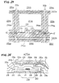
liquid crystal 540 is, as shown in Figs. 28 and 29, enclosed between a transparent substrate, in which data lines (source lines) 502a, 502b... for supplying an image signal andgate lines common electrode 533 is formed. By controlling a voltage to be applied to a position between acommon electrode 533 and apixel electrode 506 of each of the pixel regions 501aa, 501ab... via a thin-film transistor (TFT) 508, the state of orientation of the liquid crystal in each of the pixel regions 501aa, 501ab... is changed. A liquid crystal device of the foregoing type encounters a problem in that light leakage (designated by an arrow A) through a gap between, for example, thedata line 502a and thepixel electrode 506 deteriorates the quality of display. Another problem arises in that a reverse tilt domain region, in which the state of orientation of the liquid crystal disorders due to an influence of an electric field between thedata line 502a and thepixel electrode 506, is generated at a position inside the outer periphery of thepixel electrode 506 and the quality of display deteriorates due to the generated region. Therefore, in order to improve the precise clearness of the display of each pixel, a light-shieldingblack matrix 531 is formed on the othertransparent substrate 530 to correspond to a boundary region between pixel regions. Furthermore, the twotransparent substrates black matrix 531 to be positioned in the boundary region between the pixel regions so that the quality of display is maintained. If a positional deviation takes place between the boundary region between the pixel regions and theblack matrix 531, the quality of display deteriorates. Therefore, theblack matrix 531 is given a marginal width to prevent the foregoing positional deviation. - However, where the liquid crystal display device has been required to have a larger frame size and to display an image of an improved quality, the conventional arrangement that the width of the black matrix is widened to have the margin lowers the aperture ratio (the area ratio of a region capable of displaying an image) and causes a problem that the improvement in the display quality is hindered. Accordingly, the inventor of the present invention suggests an arrangement that the black matrix is formed on the transparent substrate having the matrix array formed thereon to prevent the positional deviation between the boundary region between the pixel regions and the black matrix and to set the width of the black matrix to a minimum width. The inventor of the present invention has first disclosed a liquid crystal display device described as a comparative example shown in Figs. 30 and 31. Referring to these drawings,
data lines gate lines transparent substrate 509 so that each of pixel regions 501aa, 501ab... is sectioned and formed. Along the boundary region of each of the pixel regions 501aa, 501ab... ablack matrix 517 is formed. Theblack matrix 517 is formed on the surface of aTFT 508 in, for example, a pixel region 505bb, while interposinginterlayer insulating films source 504 to which adata line 502a is electrically connected, agate electrode 505 to which agate line 503a is electrically connected, and adrain 507 to which apixel electrode 506 is electrically connected. Theblack matrix 517 is insulated and separated from each of thedata line 502a, thegate 503a and thepixel electrode 506. In the liquid crystal display device constituted as described above, each pixel region and theblack matrix 517 can be aligned to each other at an excellent accuracy while eliminating the necessity of providing unnecessary margin for the width of theblack matrix 517. Therefore, the aperture ratio of the liquid crystal device is not sacrificed. However, the liquid crystal display device encounters another problem as follows. Since no potential is applied to theblack matrix 517 and accordingly it is in a floating state, the potential of the black matrix is changed depending upon an operational state of the liquid crystal display. The potential change disorders the state of orientation of the liquid crystal present between thepixel electrode 506 and the common electrode of the other transparent substrate. As a result, the quality of display deteriorates. Since theblack matrix 517 is commonly used for each of the pixel regions 501aa, 510ab..., a short circuit taking place between theblack matrix 517 and any one of thepixel electrode 506, thedata line gate line - Accordingly, the present invention is arranged to optimize the structure of a black matrix formed on the same substrate for a matrix array so as to realize a liquid crystal display device capable of raising the aperture ratio while preventing a fact that the display quality and the reliability are sacrificed, by adapting the following means to the liquid crystal display device.
- That is, the liquid crystal display device according to the present invention is basically characterized by an arrangement comprising a first pixel region among pixel regions formed on the surface of a transparent substrate by sectioning with data lines and gate lines, wherein the first pixel region includes a thin film transistor having a source electrically connected to the data line and a gate electrode electrically connected to the gate line, a pixel electrode to which a potential can be applied via a drain of the thin film transistor, and a conductive and light shielding layer formed in a boundary region between the first pixel region and the adjoining second pixel region to constitute a black matrix, insulated and separated from the data line, the gate line and pixel electrodes of the second pixel regions, and electrically connected to the pixel electrode of the first pixel region.
- It is preferable that the conductive and light shielding layer has an outer end positioned on a boundary region between the first pixel region and the second pixel regions.
- A structure may be employed in which the first pixel region has the conductive and light shielding layer in any boundary region to the second pixel region, and the first pixel region is sectioned from the second pixel regions by the conductive and light shielding layer. Another structure may be employed in which the first pixel region has the conductive light shielding layers in two boundary regions among the boundary regions from the second pixel regions, and is sectioned from the second pixel regions by the conductive and light shielding layers and the conductive and light shielding layers that are present adjacent to two other boundary regions adjacent to the second pixel regions.
- It is preferable that substantially the overall surface of the data line is in a state it is, via an interlayer insulating film, covered with at least either the conductive and light shielding layer in the corresponding pixel region or the conductive and light shielding layer in the second pixel region adjacent via the data line.
- As for the structures of the pixel electrode and the conductive and light shielding layer, a structure may be employed in which either the pixel electrode or the conductive and light shielding layer is electrically connected to the drain via a connection hole of the interlayer insulating film, and the residual one is electrically connected to either the pixel electrode or the conductive and light shielding layer. Another structure may be employed in which the pixel electrode and the conductive and light shielding layer are formed via an upper-layer-side interlayer insulating film formed on the surface of a lower-layer-side interlayer insulating film which is the interlayer insulating film, and are electrically connected to each other via the connection hole of the upper-layer-side interlayer insulating film.
- Another structure may be employed in which either the pixel electrode or the conductive and light shielding layer is formed on the surface of the residual one and they are electrically connected. In this case, it is preferable that the outer ends of the pixel electrode and the conductive and light shielding layer substantially coincide with each other. In order to achieve this, a method of manufacturing the liquid crystal display device has an arrangement that a step of patterning a lower one of the pixel electrode and the conductive and light shielding layer is performed in a manner that the outer end of an upper layer and a mask for use in patterning the upper layer are used as masks.
- It is preferable for the present invention that either the pixel electrode or the conductive and light shielding layer is electrically connected to the drain via a stacked electrode having conductivity and electrically connected to the drain via the connection hole of the interlayer insulating film, and the residual one is electrically connected to either the pixel electrode or the conductive and light shielding layer. In this case, it is preferable that the stacked electrode layer also has light transmissivity, for example, the stacked electrode layer is made of an ITO layer.
- If the structure having the stacked electrode layer is employed, it is preferable that the outer end of the pixel electrode is extended to reach a position above the data line in terms of keeping a wide formation region.
- As for the structure of the stacked electrode layer, it is preferable that the stacked electrode layer is formed to extend to a non-formation region in which the thin film transistor is not formed, and the pixel electrode and the stacked electrode layer are electrically connected to each other in the non-formation region, that is, on a flat region to which projections and pits of the thin film transistor are not reflected.
- It is preferable that the present invention comprises the data line which includes a first data line electrically connected to the source of the thin film transistor via a first connection hole of the interlayer insulating film and a second data line electrically connected to the surface of the first data line to constitute a multi-wiring structure, and the stacked electrode layer includes a first stacked electrode layer electrically connected to the drain of the thin film transistor via a second connection hole of the interlayer insulating film and a second stacked electrode layer electrically connected to the surface of the first stacked electrode layer. In this case, it is preferable in terms of formation can be made by mutually using the processes that the first data line and the first stacked electrode layer are made of a same material, and also the second data line and the second stacked electrode layer are made of a same material.
- It is preferable that a drive circuit formed on the same substrate, on which an active matrix having the first and second pixel regions is formed, has a multi-layer wiring structure in which wiring layers are electrically connected to the interlayer insulating film formed adjacent to the active matrix via an interlayer insulating film present in the same layer in which the interlayer insulating film is formed adjacent to the active matrix.
- It is preferable that the gate electrode and the gate line according to the present invention have intrinsic polycrystalline silicon layers or polycrystalline silicon layers containing phosphorus by 1 x 10²⁰/cm³ or less and silicide layer made of high melting point metal formed on the surface of the polycrystalline silicon layer and constituting the multi-wiring structure. In this case, a method of manufacturing the liquid crystal display device comprises: a step of forming a first polycrystalline silicon film to serve as a source and drain region and a channel region on the surface of a transparent substrate; a step of forming a gate electrode insulating film on the surface of the polycrystalline silicon film; a step of depositing a second polycrystalline silicon film below the gate electrode and the gate line; a step of dispersing phosphorus in the second polycrystalline silicon film at a temperature of 850°C or lower; a step of depositing a silicide layer of high melting point metal above the gate electrode and the gate line; and a step of simultaneously patterning the second polycrystalline silicon film and the silicide layer of the high melting point metal to form the gate electrode and the gate line.
- In the present invention, in order to constitute a holding capacitance, it is preferable that at least either the pixel electrode or the conductive and light shielding layer has the outer end adjacent to the forward gate line at a position above the forward gate line to constitute an overlapping portion.
-
- Fig. 1
- is a plan view which illustrates a portion of a matrix array of a liquid crystal display device according to
Embodiment 1 of the present invention; - Fig. 2
- is a cross sectional view taken along line I-I of Fig. 1;
- Fig. 3
- is a plan view which illustrates a portion of a matrix array of a liquid crystal display device according to
Embodiment 2 of the present invention; - Fig. 4
- is a cross sectional view taken along line II-II of Fig. 3;
- Fig. 5
- is a plan view which illustrates a portion of a matrix array of a liquid crystal display device according to Embodiment 3 of the present invention;
- Fig. 6
- is a cross sectional view taken along line III-III of Fig. 5;
- Fig. 7
- is a schematic plan view which illustrates a matrix array of a liquid crystal display device according to a modification of Embodiment 3 of the present invention;
- Fig. 8
- is a plan view which illustrates a portion of a matrix array of a liquid crystal display device according to Embodiment 4 of the present invention;
- Fig. 9
- is a cross sectional view taken along line IV-IV of Fig. 8;
- Figs. 10
- (a) to (c) respectively are cross sectional views each of which illustrates a portion of a process of a method of manufacturing the liquid crystal display device shown in Fig. 8;
- Fig. 11
- is a plan view which illustrates a portion of a matrix array of a liquid crystal display device according to Embodiment 5 of the present invention;
- Fig. 12
- is a cross sectional view taken along line V-V of Fig. 11;
- Figs. 13
- (a) to (d) respectively are cross sectional views each of which illustrates a portion of a process of a method of manufacturing the liquid crystal display device shown in Fig. 11;
- Fig. 14
- is a plan view which illustrates a portion of a matrix array of a liquid crystal display device according to Embodiment 6 of the present invention;
- Fig. 15
- is a cross sectional view taken along line VI-VI of Fig. 14;
- Fig. 16
- is a plan view which illustrates a portion of a matrix array of a liquid crystal display device according to Embodiment 7 of the present invention;
- Fig. 17
- is a cross sectional view taken along line VII-VII of Fig. 16;
- Fig. 18
- is a plan view which illustrates a portion of a matrix array of a liquid crystal display device according to Embodiment 8 of the present invention;
- Fig. 19
- is a cross sectional view taken along line VIII-VIII of Fig. 18;
- Fig. 20
- is a plan view which illustrates a portion of a matrix array of a liquid crystal display device according to Embodiment 9 of the present invention;
- Fig. 21
- is a cross sectional view taken along line IX-IX of Fig. 20;
- Fig. 22
- is a plan view which illustrates a portion of a matrix array of a liquid crystal display device according to Embodiment 10 of the present invention;
- Fig. 23
- is a cross sectional view taken along line X-X of Fig. 22;
- Fig. 24
- is a plan view which illustrates a portion of a matrix array of a liquid crystal display device according to Embodiment 11 of the present invention;
- Fig. 25
- is a cross sectional view taken along line XI-XI of Fig. 24;
- Fig. 26
- is a cross sectional view which illustrates a portion of the structure of a drive circuit formed on the same substrate for the matrix array of the liquid crystal display device according to Embodiment 11 of the present invention;
- Fig. 27
- is a cross sectional view which illustrates a portion of the structure of a drive circuit formed on the same substrate for the matrix array of the liquid crystal display device according to Embodiment 11 of the present invention;
- Fig. 28
- is a plan view which illustrates a portion of a matrix array of a conventional liquid crystal display device;
- Fig. 29
- is a cross sectional view taken along line XII-XII of Fig. 28;
- Fig. 30
- is a plan view which illustrates a portion of a matrix array of a liquid crystal display device according to a comparative example of the present invention; and
- Fig. 31
- is a cross sectional view taken along line XIII-XIII of Fig. 30.
- Fig. 1 is a plan view which illustrates a portion of a matrix array of a liquid crystal display device according to
Embodiment 1 of the present invention. Fig. 2 is a cross sectional view taken along line I-I of Fig. 1. - In the liquid crystal display device according to this embodiment,
vertical data lines horizontal gate lines - Then, the structure of the pixel region will now be described while taking the pixel region 101bb (a first pixel region) for example. Pixel regions 101ab, 101ba, 101cd and 101bc (second pixel regions) are positioned adjacent to the pixel region 101bb. In the pixel region 101bb, a
TFT 108 is constituted which is constituted by asource 104, to which adata line 102a is electrically connected, agate electrode 105, to which agate line 103b is electrically connected, and adrain 107 to which apixel electrode 106 is electrically connected. Thepixel electrode 106 is a transparent electrode made of ITO and is formed on substantially overall surface of the pixel region 101bb. - As for the cross sectional structure of the
TFT 108, apolycrystalline silicon layer 110 is formed on the surface of atransparent substrate 109 for supporting the overall body of the liquid crystal display device. Thepolycrystalline silicon layer 110 to which phosphorus is doped as n-type impurity except for achannel region 111 which is a intrinsic polycrystalline silicon region. As a result, thesource 104 and thedrain 107 are formed. The phosphorus is doped by ion injection performed while using thegate electrode 105 on a gate electrode oxidizedfilm 112 as a mask in such a manner that thesource 104 and thedrain 107 are self-aligned. On the surface of theTFT 108, a lower-layer-sideinterlayer insulating film 113 made of a silicon oxide film is formed, the lower-layer-sideinterlayer insulating film 113 having afirst connection hole 113a and asecond connection hole 113b formed therein. Thedata line 102a made of a low-resistance metal layer such as an aluminum layer or an alloy layer containing aluminum is electrically connected to thesource 104 via thefirst connection hole 113a. On the other hand, apixel electrode 106 is electrically connected to thedrain 107 via thesecond connection hole 113b. - Furthermore, the liquid crystal display device according to this embodiment has an upper-layer-side
interlayer insulating film 115 formed on the surface of thetransparent substrate 109 thereof, and a chrome layer 116bb (a conductive light shielding layer) having light shielding characteristics and conductivity formed on the surface of the upper-layer-sideinterlayer insulating film 115. In the pixel region 101bb, the chrome layer 116bb is electrically connected to thepixel electrode 106 via theconnection hole 115a of the upper-layer-sideinterlayer insulating film 115 at a diagonal position to the region in which theTFT 108 is formed, that is, at an end portion in which the pixel region 101bb and the pixel regions 101ab, 101ac and 101bc are in contact with one another. The chrome region 116bb is so formed that itsouter end 116x is positioned above a boundary region between the pixel region 101bb and the pixel regions 101ab, 101ba, 101cb and 101bc, that is, above thedata lines gate lines data lines gate lines inter-layer insulating films outer end 116x of the chrome layer 116bb and the outer ends 116x of the chrome layer 116ab, 116ba, 116cb and 116bc are insulated and separated from each other above thedata lines gate lines - As a result, a potential can be applied to the chrome layer 116bb from the
pixel electrode 106 disposed in the same pixel region 101bb. However, the potential cannot be supplied from a pixel electrode in another pixel region. Furthermore, substantially the entire surface of thedata line 102a is covered with the inter-layerinsulating film 115 and the end portions of the chrome layers 116bb and 116ba so that the potential applied to thedata line 102a does not affect the liquid crystal positioned on the surface of thedata line 102a. In addition, the chrome layer 116bb is formed adjacent to theprecedent gate line 103a to have a wide overlapping area. The chrome layer 116bb is electrically connected to thepixel electrode 106. As a result, the chrome layer 116bb is in a state where it constitutes a capacitance. - This embodiment has an arrangement that the liquid crystal display device is constituted by enclosing the liquid crystal between the
transparent substrate 109, on which theblack matrix 116 is formed, and the other side transparent substrate (omitted from illustration) on which a color filter and a common electrode are formed. In response to a signal transmitted through thedata lines gate lines pixel electrode 106 is controlled. As a result, the state of orientation of the liquid crystal in each pixel region is changed to display information. - In a conventional liquid crystal display device, a black matrix corresponding to the boundary region of the pixel regions of the
transparent substrate 109 is formed on the transparent substrate having the common electrode. However, in the liquid crystal display device according to this embodiment, the fact that, for example, the chrome layer 116bb is formed in the boundary region between the pixel region 101bb and the surrounding pixel regions is utilized to use each of the chrome layers 116bb, 116ab, 116ba, 116cb, 116bc... as a black matrix. Therefore, the necessity forming the black matrix on the transparent substrate, on which the common electrode is formed, can be eliminated. Therefore, the aligning accuracy between the boundary region between the pixel regions and theblack matrix 116 required for the conventional technology does not cause a problem. Hence, the width of theblack matrix 116 can be minimized to correspond to the width of the boundary region between the pixel regions, that is, thedata lines gate lines - The chrome layer 116bb is insulated and separated from the pixel electrodes of the
data lines gate lines pixel electrode 106 in the same pixel region 101bb. Therefore, the potential of the chrome layer 116bb is in a state where the same potential as that of thepixel electrode 106 is always supplied regardless of the state of the operation of the liquid crystal display device. As a result, the potential of the chrome layer 116bb does not disorder the state of orientation of the liquid crystal present in the pixel region 101bb between thepixel electrode 106 and the common electrode. Therefore, excellent display quality can be obtained. Furthermore, theblack matrix 116 is composed of the chrome layers 116b... which are electrically independent in each pixel region. If, for example, the chrome layer 116bb and thedata line 102a are in a short-circuit state in the pixel region 101bb, only the pixel region 101bb cannot display an image, that is, the influence of the short circuit causes only a point display defect. Therefore, the reliability of the liquid crystal display device is satisfactory. -
- Fig. 3 is a plan view which illustrates a portion of a matrix array of a liquid crystal display device according to
Embodiment 2 of the present invention. Fig. 4 is a cross sectional view taken along line II-II of Fig. 3. The elements having the same functions as those of the elements of the liquid crystal display device according toEmbodiment 1 are given the same reference numerals and their detailed descriptions are omitted here. - Also in the liquid crystal display device according to this embodiment, the
TFT 108 is formed on the surface of thetransparent substrate 109 in, for example, the pixel region 101bb (the first pixel region) among the pixel regions 101aa, 101ab, 101ac, 101ba, 101bb... formed by sectioning performed by wiring thevertical data lines horizontal gate lines interlayer insulating film 113 made of a silicon oxide film is deposited on the surface of theTFT 108. Thedata line 102a is electrically connected to thesource 104 via thefirst connection hole 113a. Furthermore, the upper-sideinterlayer insulating film 115 is formed on their surfaces. The chrome layer 116bb (the conductive light shielding layer) having light shielding characteristics and conductivity is electrically connected to thedrain 107 via theconnection hole 115a which penetrates the foregoing first and upper-sideinterlayer insulating films pixel electrode 106 to be applied with the potential via the drain is electrically connected to the chrome layer 116bb formed on the surface of the upper-sideinterlayer insulating film 115. Similarly toEmbodiment 1, the chrome layer 116bb is so formed that itsouter end 116x is positioned above the boundary region between the pixel region 101bb and the adjacent pixel regions 101ab, 101ba, 101cb and 101cb (the second pixel regions), that is, on the regions in which thedata lines gate lines data lines gate lines interlayer insulating films pixel electrode 106 in the same pixel region 101bb. The surface side of thedata line 102a is covered with the interlayerinsulting film 115 and the end portions of the chrome layers 116bb and 116ba so that the potential applied to thedata line 102a does not affect the liquid crystal placed on the surface of thedata line 102a. - Also in the liquid crystal display device constituted as described above, the
black matrix 116 is, in addition to the matrix array, formed on thetransparent substrate 109 to correspond to the boundary region between the pixel regions. Therefore, the width of the black matrix can be set to a minimum width, resulting in a high aperture ratio of the liquid crystal display device. Furthermore, the chrome layer 116bb is electrically connected to only thepixel electrode 106 in the same pixel region 101bb, resulting in a state being realized where the same potential as that of thepixel electrode 106 is applied to the chrome layer 116bb, regardless of the state of the operation of the liquid crystal display device. Therefore, the potential of the chrome layer 116bb does not disorder the state of the orientation of the liquid crystal present between thepixel electrode 106 and the common electrode. Since all of the chrome layers respectively are independent in the corresponding pixel regions, even if the chrome layer and a data line or the like are short-circuited in one pixel region 101bb, the influence of this causes only a point defect to occur in display. Therefore, the excellent reliability of the liquid crystal display device can be maintained. -
- Fig. 5 is a plan view which illustrates a portion of a matrix array of a liquid crystal display device according to a third embodiment of the present invention. Fig. 6 is a cross sectional view taken along line III-III of Fig. 5. Elements having functions corresponding to the elements of the liquid crystal display device according to
Embodiment 1 are given the same reference numerals and their detailed descriptions are omitted here. - Also in the liquid crystal display device according to this embodiment, the
data line 102a is electrically connected to thesource 104 of theTFT 108 formed on the surface of thetransparent electrode 109 in the pixel region 101bb (the first pixel region) via theconnection hole 113a of the lower-sideinterlayer insulating film 113. On the other hand thepixel electrode 106 is electrically connected to thedrain 107 via the upper-sideinterlayer insulating film 113b. The chrome layer 116bb formed on the surface of the upper-sideinterlayer insulating film 115 is electrically connected to thepixel electrode 106 via theconnection hole 115a. - In this embodiment, the
outer end 116x of the chrome layer 116bb is beyond thedata line 102a and thegate line 103a to extend into the adjacent pixel regions 101ba and 101cb. On the other hand, in the pixel region 101bb, the chrome layer 116bb is not formed in the boundary region between the pixel region 101bb and the adjacent pixel regions 101bc and 101ab. The chrome layer 116bb is formed into an L-shape on the adjacent boundary regions. In the boundary region of the pixel region 101bb adjacent to the pixel region 101bc, the end portion of the chrome layer 116bc formed in the pixel region 101bc is beyond thedata line 102b to be extended into the pixel region 101bb. In the boundary region of the pixel region 101bb adjacent to the pixel region 101ab, the end portion of the chrome layer 116ab formed in the pixel region 101ab is beyond thegate line 103b to be extended into the pixel region 101bb. As a result, the pixel region 101bb is formed by sectioning with the chrome layer 116bb formed to correspond to the pixel region 101bb and the chrome layers 116bc and 116ab formed to correspond to the adjacent pixel regions 101bc and 101ab. - In this embodiment, the fact that the chrome layers 116bb, 116bc, 116ab... section the pixel regions 101bb... is utilized to use the chrome layers 116bb... as the
black matrix 116. - Therefore, the aperture ratio of the liquid crystal display device according to this embodiment is raised. Furthermore, the
black matrix 116 is not in the floating state, resulting in that its potential does not disorder the liquid crystal. In addition, theblack matrix 116 is constituted by the chrome layers 116bb, 116bc, 116ab... which are electrically independent in each pixel region, resulting in that the influence of short-circuit one of the chrome layers 116bb, 116bc, 116ab... causes only a point defect in display. - This embodiment is different from the liquid crystal displays according to
Embodiment 1 andEmbodiment 2 in that the end portions of the chrome layers 116bb, 116bc, 116ab... are not formed adjacently over a wide range on thedata lines gate line black matrix 116 is formed, their short-circuit is prevented. Furthermore, thepixel region 106 is formed on the surface of theinterlayer insulating film 113, while the chrome layers 116bb, 116bc, 116ab... are formed on the surface of theinterlayer insulating film 115. That is, thepixel region 106 and chrome layers 116bb, 116bc, 116ab... in the adjacent region are formed in different layers. Therefore, even if they are disposed adjacently, no short-circuit takes place. As a result, theblack matrix 116 composed of the chrome layers 116bb, 116bc, 116ab... electrically independent in each pixel region can easily be formed. - In Embodiment 3, the structure is so arranged that the chrome layers 116bb, 116bc, 116ab...serving as the conductive light shielding layers are disposed in the two boundary regions among the boundary regions of adjacent pixel regions. The pixel region is sectioned by the foregoing chrome layer and the adjacent chrome layers in the pixel regions adjacent to the chrome layer at the other two boundary regions. A modification of Embodiment 3 may be employed in which the
black matrix 116 is so formed as shown in Fig. 7 that chrome layers 118ab, 118bc, 119ab, 119bc serving as the conductive light shielding layers are formed in facing two boundary regions among the boundary regions of the adjacent pixel regions while changing the direction in each adjacent pixel region. In this case, the chrome layers 118ab, 118bc, 119ab, 119bc... respectively are electrically connected to the pixel regions 101aa, 101ab, 101ac... positioned in directions designated by "→" shown in Fig. 7. - The shape, structure, material and the like of each element for constituting the liquid crystal display device must be set to predetermined conditions depending upon the size and the purpose of the liquid crystal display device to be manufactured. Therefore, they are not limited.
- Although the chrome layer is employed as the conductive light shielding layer for constituting the black matrix in each embodiment, the material of it is not limited. A metal layer such as titanium or aluminum, a silicon layer, or silicide compound such as molybdenum silicide or tungsten silicide may be used if the material has conductivity and the light shielding characteristics.
-
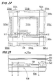
- Fig. 8 is a schematic plan view which illustrates an active matrix substrate for use in a liquid crystal display device according to Embodiment 4 of the present invention. Fig. 9 is a cross sectional view taken along line IV-IV of Fig. 8.
- Also in the liquid crystal display device according to this embodiment,
vertical data lines horizontal gate lines Embodiment 1. Pixel regions 201aa, 201ab, 201ac... are, by sectioning, formed between the foregoing lines. Then, the structure will now be described while taking the pixel region 201bb (a first pixel region) for example. Acolor filter 232 for enabling color display, acommon electrode 233 and an opposing-substrate-side orienting film 234 are formed on an opposing-substrate- 230 shown in Fig. 9. Furthermore, an opposing substrate sideblack matrix 231 is formed on the opposingsubstrate 230. In the liquid crystal display device according to this embodiment, another black matrix is formed on the active matrix substrate as described later. The opposing-substrate-sideblack matrix 231 is provided for the purpose of complementing the black matrix formed on the active matrix substrate. - As shown in Fig. 8, the pixel regions 201ab, 201ba, 201cb, 201bc (a second pixel region) are formed adjacent to the pixel region 210bb (the first pixel region). In the pixel region 201bb, a
TFT 208 is constituted by asource 204 to which thedata line 202a is electrically connected, agate electrode 205 to which thegate line 203b is electrically connected, and adrain 207 to which apixel electrode 206 is electrically connected. Thepixel electrode 206 is a transparent electrode made of ITO which is a conductive and light transmissible material, thepixel electrode 206 being formed on substantially the whole surface in the pixel region 201bb. The end portions of thepixel electrode 206 are extended to positions above thedata lines gate line pixel electrode 206 has a wide overlapping area on theforward gate line 203a. - As for the cross sectional structure of the
TFT 208, apolycrystalline silicon layer 210 is, as shown in Fig. 9, formed on the surface of atransparent substrate 209 supporting the overall body of the liquid crystal display device. - The
polycrystalline silicon layer 210 to which phosphorus is, as n-type impurity, doped except for achannel region 211 which is a intrinsic polycrystalline silicon region. As a result, thesource 204 and thedrain 207 are formed. On the surface of theTFT 208, a lower-layer-sideinterlayer insulating film 213 made of a silicon oxide film is formed, the lower-layer-sideinterlayer insulating film 213 having afirst connection hole 213a. Thedata line 202a made of an aluminum layer is electrically connected to thesource 204 via thefirst connection hole 213a. - Furthermore, the liquid crystal display device according to this embodiment has an upper-layer-side
interlayer insulating film 215 formed on the surface of the lower-layer-sideinterlayer insulating film 213. The upper-layer-sideinterlayer insulating film 215 and the lower-layer-sideinterlayer insulating film 213 have asecond connection hole 215a. Apixel electrode 206 is electrically connected to thedrain 207 via thesecond connection hole 215a. Thepixel electrode 206 is so formed in the pixel region 201bb and adjacent pixel regions 201ab, 201ba, 201bc and 201cb that its outer end 206c is positioned above thedata lines gate lines - In the liquid crystal display device according to this embodiment, a molybdenum silicide layer 216bb (a conductive and light shielding layer) is formed on the surface of the upper-layer-side
interlayer insulating film 215 and as well as below thepixel electrode 206. The molybdenum silicide layer 216bb is so formed that itsouter end 216x is positioned above thedata lines gate lines end 206x of thepixel electrode 206. - The conductive and light shielding layer such as the molybdenum silicide layer 216bb is similarly formed in each of the pixel regions. The molybdenum silicide layer 216bb is in a state where it is insulated and separated from the
outer end 216x of each of the molybdenum silicide layers 216ab, 216ba, 216cb and 216c in the adjacent pixel regions 201ab, 201ba, 201cb and 201bc at positions above thedata lines gate lines pixel electrode 206 in the same pixel region 201bb. However, the potential is not applied from any pixel electrode in the other pixel regions. In addition, substantially the whole surface of thedata line 202a is covered with theinterlayer insulating film 215, the end portions of the molybdenum silicide layers 216bb and 216ba and the end portion of thepixel electrode 206, resulting in that the potential applied to thedata line 202a does not affect the liquid crystal placed on the surface of thedata line 202a. - The liquid crystal is enclosed between the active matrix and the opposing
substrate 230, the active matrix being structured as described above and formed on the surface of thetransparent substrate 209 in a state where an orientingfilm 220 is formed on the surface of thepixel electrode 206 and the molybdenum silicide layer 216bb. As a result, display utilizing the orientation of the liquid crystal is enabled. - In the liquid crystal display device constituted as described above, each of the molybdenum silicide layers 216bb, 216ab, 216ba... is utilized as the
black matrix 216, resulting in that the necessity of providing the black matrix on the opposingsubstrate 230 can be eliminated if the data line and the gate line have the light shielding characteristics. If the data line or the gate line does not have the light shielding characteristics, only a complementary black matrix such as theblack matrix 231 on the opposing substrate as shown in Fig. 9 is required. Therefore, the width of theblack matrix 216 or that of theblack matrix 231 on the opposing-side substrate does not need to be widened excessively in order to improve the position alignment accuracy at the time of allowing the two transparent substrates to face each other. Since each of the molybdenum silicide layers 216bb, 216ab... is formed to reach the surface of the same transparent substrate of the pixel regions 201bb, 201ab... accuracies in terms of position alignment can be improved. Therefore, the width can be set to a minimum value to correspond to the width of each of thedata lines gate lines pixel electrode 206 is always applied, thus resulting in that the potential of the molybdenum silicide layer 216bb does not disorder the state of orientation of the liquid crystal. As a result, excellent display quality can be obtained. - Even if both of the
pixel electrode 206 and theblack matrix 216 act as the electrodes, the outer surface range of thepixel electrode 206 and that of theblack matrix 216 can be made to coincide with each other. Therefore, a region (a reverse tilt domain region), in which the orientation of the liquid crystal is disordered due to an undesirable influence of the potential from the foregoing electrodes, can be assuredly covered with theblack matrix 216. Furthermore, theblack matrix 216 is constituted by the molybdenum silicide layers 216bb... each of which is electrically independent in each pixel region, thus resulting in that only a point defect of the pixel region 201bb takes place even if short circuit occurs between the molybdenum silicide layer 216bb and thedata line 202a. As a result, excellent reliability can be attained from the liquid crystal display device. - Furthermore, the pixel region 201bb is formed precisely due to the tendency of precisely forming the liquid crystal display device, thus resulting in the display capacitance in the pixel region 201bb being reduced. Even if the leak current is decreased by constituting the
TFT 208 having a large off-resistance, the display voltage is lowered in a period in which thegate line 203b is not selected Therefore, the display maintaining characteristics tends to deteriorate. However, the liquid crystal display device according to this embodiment is so arranged that the end portion of thepixel electrode 206 is positioned above theforward gate line 203a so that a charge storage capacitance is formed by them. Therefore, theforward gate line 203a is in a non-selected state during a period in which the pixel region 201bb is being selected, and a reference voltage is accordingly applied to thegate line 203a. By utilizing this fact, characteristics for maintaining the voltage applied to the liquid crystal in the pixel region 201bb can be improved by storing a charge in the charge storage capacitance. - Then, a portion of a method of manufacturing the liquid crystal display device according to this embodiment will be described while making a reference to the left portion of the regions shown in Figs. 10 (a) to (c). Figs. 10 (a) to (c) are cross sectional views which illustrate a portion of the process for manufacturing the liquid crystal display device according to this embodiment.
- Since a known method can be employed until the
TFT 208 is formed on thetransparent substrate 209 as shown in Fig. 10 (a), the description about it is omitted. After theTFT 208 has been formed, the lower-layer-sideinterlayer insulating film 213 is formed. Then, thefirst connection hole 213a is formed, and thedata line 202a made of the aluminum layer is formed to connect electrically thedata line 202a to thesource 204 of theTFT 208. Then, the upper-layer-sideinterlayer insulating film 215 is formed on the surface of the lower-layer-sideinterlayer insulating film 213 followed by forming of thesecond connection hole 215 in the upper-layer-sideinterlayer insulating film 215. - Then, the molybdenum silicide layer is deposited, and then it is patterned as shown in Fig. 10 (b) to form the
molybdenum silicide layer 216a. In this state, themolybdenum silicide layer 216a is not in a state where it has the pattern to constitute theblack matrix 216. - Then, an
ITO layer 206a is formed on the surface of themolybdenum silicide layer 216a, and then theITO layer 206 is patterned to form thepixel electrode 206 as shown in Fig. 10 (c). Then, a mask used at the time of forming thepixel electrode 206 by patterning is used as it is to pattern themolybdenum silicide layer 216a while using thepixel electrode 206 as the mask. As a result, the molybdenum silicide layer 216bb for constituting theblack matrix 216 is formed. In the process of patterning the lower layers among thepixel electrode 206 and the molybdenum silicide layer 216bb, the outer end of the upper layer or the mask used to pattern the upper layer is, as described above, used as the mask at the time of performing patterning. - As a result, a structure can be constituted in which the
outer end 206x of thepixel electrode 206 and theouter end 216x of the molybdenum silicide layer 216bb can be allowed to coincide with each other, and they are positioned above thedata line 202a. Since a known process can be employed to perform the following process, its description is omitted here. - As described above, the method of manufacturing the liquid crystal display device according to this embodiment has an arrangement that the
pixel electrode 206 is so formed by patterning that themolybdenum silicide layer 216a is present below thepixel electrode 206 to protect the lower layer. Therefore, if an etchant of a chloride type is used to pattern theITO layer 206, a pit or the like of the upper-layer-sideinterlayer insulating film 216 does not cause the lower data line 202 constituted by the aluminum layer to be damaged by the etchant. Therefore, thedata line 202a can be freed from disconnection or the like, the reliability of the liquid crystal display device can be improved. - The cross sectional view showing the manufacturing process in the right portion of each of Figs. 10 (a) to (c) illustrates a modification of the foregoing manufacturing method.
- That is, the
molybdenum silicide layer 216a is left in thesecond connection hole 215a as shown in Fig. 10 (b), causing thepixel electrode 206 made of the ITO layer to be electrically connected, via the molybdenum silicide layer 216bb, to thedrain region 207 made of silicon after thepixel electrode 206 has been formed. As a result, the contact resistance can be reduced as compared with a case where thepixel electrode 206 and thedrain region 107 are directly connected to each other, thus resulting in the display quality to be improved. - Although the active matrix substrate formed by either of the manufacturing methods shown in the right and the left regions of Figs. 13 (a) to 13 (c) is constituted such that the
pixel region 206 is formed above theblack matrix 216, the present invention is not limited to this. A structure may be employed in which the vertical positional relationship between thepixel region 206 and theblack matrix 216 is inverted. - Fig. 11 is a schematic plan view which illustrates a portion of an active matrix substrate for use in the liquid crystal display device according to Embodiment 5 of the present invention. Fig. 12 is a cross sectional view taken along line V-V of Fig. 11. Elements having functions corresponding to those of the elements of the liquid crystal display device according to Embodiment 4 shown in Figs. 8 and 9 are given the same reference numerals, and their detailed descriptions are omitted here.
- Also in the liquid crystal display device according to this embodiment, pixel regions 201ab, 201ba, 201cb and 201bc (second pixel regions) are positioned adjacent to the pixel region 201bb (the first pixel region). In the pixel region 201bb, the
TFT 208 is constituted by thesource 204, thegate electrode 205 and thedrain 207. The lower-layer-sideinterlayer insulating film 213 made of a silicon oxide film is deposited on the surface of theTFT 208. The lower-layer-sideinterlayer insulating film 213 has thefirst connection hole 213a and thesecond connection hole 213b formed therein. Thedata line 202a made of the aluminum layer is electrically connected to thesource 204 via thefirst connection hole 213a, while thepixel electrode 206 made of the ITO layer is electrically connected to thedrain 207 via thesecond connection hole 213b. - The
pixel electrode 206 is formed to reach positions adjacent to the boundary regions between the pixel region 201bb and adjacent pixel regions 201ab, 201ba, 201bc and 201cb. Itsouter end 206x is positioned inside the positions at which thedata lines gate lines pixel electrode 206. Also the molybdenum silicide layer 216bb is formed to reach positions adjacent to the boundary regions between the pixel region 201bb and adjacent pixel regions 201ab, 201ba, 201bc and 201cb. Itsouter end 216x is positioned inside the positions at which thedata lines gate lines outer end 206x of thepixel electrode 206. As for the width of the molybdenum silicide layer 216bb, it is preferable that the side of the molybdenum silicide layer, where the orientation of the liquid crystal can easily be disordered in the pixel region 201bb, has a thick width and the other side where disordering cannot easily take place has a narrow width. Accordingly, the liquid crystal display device according to this embodiment has an arrangement to shield from light the reverse tilt domain region in which the orientation of the liquid crystal adjacent to thedata line 202a is disordered by an influence of the charge of thedata line 202a, the arrangement being made such that the width W1 of side of the molybdenum silicide layer 216bb adjacent to thedata line 202a is made to be thicker than the width W2 of the side adjacent to thedata line 202b. Thus, even if the alignment is deviated, the reverse tilt domain region can be assuredly covered, resulting in the display quality to be maintained and the reduction in the aperture ratio to be minimized. - Since the liquid crystal display device constituted as described has an arrangement that each of the molybdenum silicide layers 216bb... is utilized as the black matrix, the molybdenum silicide layer 216bb serves as a margin at the time of the position alignment of the opposing-substrate-side
black matrix 231 at the time of causing the side of the active matrix constituted adjacent to thetransparent substrate 209 and the side of the opposingsubstrate 230 to face each other. Therefore, accuracy in the position alignment can be disregarded. Furthermore, the potential of the molybdenum silicide layer 216bb is in a state where the same potential as that of thepixel electrode 206 is applied, resulting in that the state of the orientation of the liquid crystal cannot be disordered. Therefore, excellent display quality can be obtained. In addition, theblack matrix 216 is constituted by the molybdenum silicide layers 216bb... which are electrically independent from one another in each pixel region. Therefore, a short circuit occurring in the pixel region 201bb between the molybdenum silicide layer 216bb and thedata line 202a will cause only a point defect to occur in the display performed by the pixel region 201bb. As a result, the reliability of the liquid crystal display device is excellent. - Referring to the left portions of the portions shown in Figs. 13 (a) to (d), a portion of a method of manufacturing the liquid crystal display device according to the present invention will now be described. Figs. 13 (a) to (d) are cross sectional views which illustrate a portion of a manufacturing process of the method of manufacturing the liquid crystal display device according to this embodiment.
- Since a known method can be employed in the process until the
TFT 208 is formed on thetransparent substrate 209 as shown in Fig. 13 (a), its description is omitted here. After theTFT 208 has been formed, the lower-layer-sideinterlayer insulating film 213 is deposited followed by forming thefirst connection hole 213a and thesecond connection hole 213b in the lower-layer-sideinterlayer insulating film 213. Then, theITO layer 206a to form thepixel electrode 206 is formed by sputtering. - As shown in Fig. 13 (b), the
molybdenum silicide layer 216a is then deposited, and then only themolybdenum silicide layer 216a is patterned. In this state, themolybdenum silicide layer 216a has not been patterned to have a pattern constituting theblack matrix 216. Also theITO layer 206a has not been patterned to have a pattern constituting thepixel electrode 206. - Then, as shown in Fig. 13 (c), the edge of the
molybdenum silicide layer 216a is patterned prior to patterning theITO layer 206a to form themolybdenum silicide layer 216b constituting the black matrix. Then, by using the same mask as it is, theITO layer 206a is patterned so that thepixel electrode 206 is formed. In order to maintain excellent etching accuracy, themolybdenum silicide layer 216a is subjected to plasma etching with CF4 gas, while theITO layer 206a is, following the plasma etching of themolybdenum silicide layer 216a, subjected to anisotropic etching by using a mixture gas of CH₄ gas and H₂ gas. As a result, the outer ends 206x and 216x of thepixel electrode 206 and the molybdenum silicide layer 216bb coincide with each other in portions adjacent to the boundary regions between the pixel region 201bb and the adjacent pixel regions 201ab, 201ba, 201bc and 201cb. The plasma etching with the CF₄ gas may be performed similarly by using a molybdenum silicide layer or a tungsten silicide layer in place of themolybdenum silicide layer 216a. - Then, the aluminum layers for forming the
data lines data line 202a to be formed. - Since a know process may be employed to perform the ensuing process, its description is omitted.
- As described above, according to the method of manufacturing the liquid crystal display device according to the present invention, the outer surface range of the
pixel electrode 206 and the outer surface range of theblack matrix 216 can be made to coincide with each other even if both of thepixel electrode 206 and theblack matrix 216 act as the electrodes. Therefore, the disorder of the orientation of the liquid crystal caused by the potential from the foregoing electrodes can be assuredly covered with theblack matrix 216. - The cross sectional views which illustrates the process shown in the right portions of the portions shown in Figs. 13 (a) to (d) illustrate a modification of the aforesaid manufacturing method.
- That is, as shown in Fig. 13 (b), the
ITO layer 206a is formed on the lower-layer-sideinsulating film 213 in a region a-1 and a region a-2 in which the lower-layer-sideinterlayer insulating film 213 has been formed. Then, thefirst connection hole 213a and thesecond connection hole 213b are formed. - Then, the
molybdenum silicide layer 216a is formed as shown in Fig. 13 (b). As a result, a state is realized in which themolybdenum silicide layer 216a is electrically connected to thesource 204 and thedrain 207 of theTFT 208. Then, themolybdenum silicide layer 216a is patterned as shown in Fig. 13 (c) so that the molybdenum silicide layer 216bb constituting theblack matrix 216 is formed. Furthermore, the molybdenum silicide layers 216b and 216c are left in thefirst connection hole ITO layer 206a so that thepixel electrode 206 is formed. As a result, a structure is formed in which the outer ends 206x and 216x of thepixel electrode 206 and the molybdenum silicide layer 16bb coincide with each other at positions adjacent to the boundary regions between the pixel region 201bb and adjacent pixel regions 201ab, 201ba, 201bc and 201cb. - Then, the
data line 202a is formed on the surface of the molybdenum silicide layer 216bb in a region d-1 as shown in Fig. 13 (d) so that a structure is formed in which thedata line 202a is electrically connected to thesource 204 via themolybdenum silicide layer 216b. - Since a known process may be employed to perform the ensuing process, its description is omitted.
- The aforesaid manufacturing method causes the
data line 202a made of the aluminum layer to be connected to thesource 204 made of silicon via the molybdenum silicide layer 206b, resulting in the invasion of the silicon by an eutectic reaction with aluminum to be prevented. As a result, theTFT 208 can be formed from a thin silicon film, resulting in an improvement in the ON/OFF ratio. - In the region d-2 shown in Fig. 13 (d), the
pixel electrode 206 made of the ITO layer and thedrain 207 made of silicon are electrically connected via themolybdenum silicide layer 206a. Therefore, the contact resistance can be reduced as compared with a case where thepixel electrode 206 and thedrain 207 are directly connected to each other. As a result, the display quality can be improved. - Although the
pixel region 206 is formed below theblack matrix 216 in either case of the manufacturing methods shown in the right and the left regions of Figs. 13 (a) to 13 (d), the present invention is not limited to this. An inverted structure may be employed. - Fig. 14 is a schematic plan view which illustrates a portion of an active matrix substrate for use in a liquid crystal display device according to Embodiment 4 of the present invention. Fig. 15 is a cross sectional view taken along line VI-VI of Fig. 14.
- The liquid crystal display device according to this embodiment has the basic structure similar to that of the liquid crystal display device according to Embodiment 4. There is a difference in only the type of the liquid crystal to be enclosed between the active matrix and the opposing substrate. Hence, the same reference numerals are given to the corresponding elements and their detailed descriptions are omitted here.
- Referring to the foregoing drawings, the liquid crystal display device according to this embodiment also includes the molybdenum silicide layer 216bb (a conductive and light shielding layer) having the light shielding characteristics and conductivity on the surface of the
pixel electrode 206 in the pixel region 201. The molybdenum silicide layer 216bb is so present in the boundary regions between the pixel region 201bb and the adjacent pixel regions 201ab, 201ba, 201bc and 201cb that itsouter end 216c coincides with the outer end 206c of thepixel electrode 206 above thedata lines gate lines - The opposing
substrate 230 is disposed to face the active matrix substrate constituted as described above. Furthermore,liquid crystal 241 is enclosed between the forgoing substrates. Since a polymer-dispersion-type liquid crystal is enclosed in the liquid crystal display device according to this embodiment, the orienting film is not formed on the surface of the active matrix substrate and the opposingsubstrate 230. The residual structures are the same as those of the liquid crystal display device according to Embodiment 4. - Although the liquid crystal display device according to this embodiment is different in the type of the liquid crystal from the liquid crystal display device according to Embodiment 4, each of the molybdenum silicide layers 216bb, 216ab, 216ba... is used as the
black matrix 216. Therefore, the black matrix does not need to be provided on the opposingsubstrate 230,or the opposing-substrate-sideblack matrix 231 may be complementarily formed as shown in Fig. 15. As a result, the accuracy in the position alignment can be regarded at the time of allowing the two transparent substrates to face each other. Therefore, the necessity of providing unnecessary margin for the width of theblack matrix 216 and theblack matrix 231 on the opposing substrate can be eliminated. As a result, effects such as that the aperture ratio of the liquid crystal display device can be raised can be obtained similarly to the liquid crystal display device according to Embodiment 4. - Fig. 16 is a schematic plan view which illustrates a portion of an active matrix substrate for use in a liquid crystal display device according to Embodiment 7 of the present invention. Fig. 17 is a cross sectional view taken along line VII-VII of Fig. 18.
- Also in the liquid crystal display device according to this embodiment, a
TFT 308 is constituted by asource 311a to which adata line 302a is electrically connected and adrain 311b to which apixel electrode 306 is electrically connected in any pixel region such as a pixel region 301bb (a first pixel region) which are formed by sectioning withvertical data lines horizontal gate lines TFT 308 is arranged similarly to the TFT of the liquid crystal display device according toEmbodiment 1 in terms of the function, the liquid crystal display device according to the present embodiment has an arrangement that it is constituted by a so-called inverted stagger type TFT. That is, an insulating film is formed on the surface of atransparent substrate 309 supporting the overall body of the liquid crystal display device. Furthermore, agate electrode 305 is formed on the surface of the insulating film. Furthermore, a gateelectrode insulating film 305a, a non-doped amorphous silicon layer 310, and amorphous silicon layers (sources source electrode 304a and adrain electrode 307a are formed to correspond to the amorphous silicon layer (thesource pixel electrode 306 is electrically connected to thedrain electrode 307a via aninterlayer insulating film 313. - The liquid crystal display device according to this embodiment has a molybdenum silicide layer 316bb (a conductive and light shielding layer) formed on the surface of the
interlayer insulating film 313 and as well as below thepixel electrode 306. The molybdenum silicide layer 316bb is so formed in the boundary regions between the pixel region 301bb and adjacent pixel regions 301ab, 301ba, 301bc and 301cb that itsouter end 306x is positioned above thedata lines gate lines - Although the liquid crystal display device structured as described above is different in the structure from the liquid crystal display device according to Embodiment 4 due to the difference in the structure from the
TFT 308, a similar principle of the display is employed. As a result, a similar effect to that obtainable from the liquid crystal display device according to Embodiment 4 can be attained. For example, the molybdenum silicide layers 316bb,.. formed in each of the pixel regions 301bb... is used as theblack matrix 316, resulting in that the black matrix does not need to be formed on an opposingsubstrate 330, or only a complementary element for shielding only light that passes through thedata lines active matrix 331 shown in Fig. 17. Therefore, the necessity of unnecessarily widening the width of theblack matrix 316 or the opposing substrate sideactive matrix 331 for improving the position alignment at the time of allowing the two transparent substrates to face each other can be eliminated. Furthermore, each of the molybdenum silicide layers 316bb... are formed to reach the surface of the same transparent substrate in the pixel regions 301bb,..resulting in an excellent accuracy in terms of the position. Accordingly, the width of the molybdenum silicide layers 316bb,,, can be set to a minimum width to correspond to the width of each of thedata lines 302a, 302, thegate lines pixel electrode 306 and the outer surface range of theblack matrix 316 can be made to coincide with each other, thus resulting in an effect to be obtained that the potential from the foregoing electrodes causing the disorder of the orientation of the liquid crystal can be assuredly covered with theblack matrix 316. - Fig. 18 is a schematic plan view which illustrates a portion of an active matrix substrate for use in a liquid crystal display device according to Embodiment 8 of the present invention. Fig. 19 is a cross sectional view taken along line VIII-VIII of Fig. 18. Elements having functions corresponding to those of the elements of the liquid crystal display device according to Embodiment 4 shown in Figs. 8 and 9 are given the same reference numerals.
- Also in the liquid crystal display device according to this embodiment, the
TFT 208 is, as shown in Fig. 18, formed in the pixel region 201bb (the first pixel region) by thesource 204 to which thedata line 202a is electrically connected, thegate electrode 205 to which thegate line 203b is electrically connected, and thedrain 207 to which thepixel electrode 206 is electrically connected. Thepixel electrode 206 is a transparent electrode made of ITO which is a conductive and light transmissible material, and is formed over the whole surface of the pixel region 201bb. The end portion of thepixel electrode 206 is extended to position above thedata lines 202a 202b, thegate lines pixel electrodes 206 has a wide overlapping area over theforward gate line 203a. - As for the cross sectional structure of the pixel region 201bb, phosphorus is, as the n-type impurity, doped to the
polycrystalline silicon layer 210 formed on the surface of thetransparent substrate 209 supporting the whole body of the liquid crystal display device except for thechannel region 211 so that thesource 204 and thedrain 207 are formed. A lower-layer-sideinterlayer insulating film 213 made of a silicon oxide film is deposited on the surface of theTFT 208. Thefirst connection hole 213a and thesecond connection hole 213b are formed in the lower-layer-sideinterlayer insulating film 213. Thedata line 202a made of the aluminum layer is electrically connected to thesource 204 via thefirst connection hole 213a. - A
stacked electrode layer 214 made of ITO, which is a conductive and light transmissible material, similarly to thepixel electrode 206 is electrically connected to thedrain 207 via thesecond connection hole 213b. The surface of the lower-layer-sideinterlayer insulating film 213 has projections and pits reflecting the shape of theTFT 208, while the stackedelectrode 214 is formed to extend onto aflat region 208a (on a region in which theTFT 208 is not formed) in which theTFT 208 is not formed. Therefore, the surface of the stackedelectrode 214 is flat in thisregion 208a. - Furthermore, in the liquid crystal display device, the upper-layer-side
interlayer insulating film 215 made of a silicon oxide film is formed on the surface of thetransparent substrate 209. Thepixel electrode 206 is formed on the surface of the upper-layer-sideinterlayer insulating film 215. Thepixel electrode 206 is electrically connected to the stackedelectrode layer 214 via theconnection hole 215a of the upper-layer-sideinterlayer insulating film 215. Theconnection hole 215a is formed on theflat region 208a in which theTFT 208 is not formed. As a result, thepixel electrode 206 is electrically connected to the flat region of the stackedelectrode layer 214. Incidentally, a polyimide layer or the like may be employed as the upper-layer-sideinterlayer insulating film 215 to flatten its surface for the purpose of further improving the orienting characteristics of the liquid crystal. - This embodiment has an arrangement that liquid crystal is enclosed between the
transparent substrate 209 on which the matrix array is formed and the other side transparent substrate (omitted from illustration) on which a color filter and a common electrode are formed so that a liquid crystal display device is constituted. In response to a signal transmitted through thedata lines gate lines pixel electrode 206 is controlled to change the state of orientation of the liquid crystal in each pixel region, causing information to be displayed. The potential is applied to thepixel electrode 206 via thedrain 207 and the stackedelectrode layer 215 of theTFT 208. - In the liquid crystal display device according to this embodiment, the molybdenum silicide layer 216bb (the conductive and light shielding layer) having light shielding characteristics and conductivity is formed on the surface of the upper-layer-side
interlayer insulating film 215 and as well as below thepixel electrode 206. The molybdenum silicide layer 216bb is so formed that itsouter end 216c is positioned above thedata lines gate lines outer end 216x coincides with theouter end 206x. The conductive and light shielding layer such as the molybdenum silicide layer is similarly formed in any pixel region. The molybdenum silicide layer 216bb is insulated and separated from the outer ends 216c of each of the molybdenum silicide layers 216ab, 216ba, 216cb and 216bc in the adjacent pixel regions 201ab, 201ba, 201cb and 201bc at positions above thedata lines gate lines - In the liquid crystal display device constituted as described above, each of the molybdenum silicide layers 216bb... is used as the black matrix. Therefore, when the active matrix substrate formed on the
transparent substrate 209 and the opposingsubstrate 230 are allowed to face each other as shown is Fig. 12, the molybdenum silicide layer 216bb serves as a margin at the time of the position aligning of theblack matrix 231 on the opposing substrate. As a result, the position aligning accuracy is not critical. Furthermore, the potential of the molybdenum silicide layer 216bb is in a state where the same potential as thepixel electrode 206 is applied, resulting in that the state of the orientation of the liquid crystal is not disordered. As a result, excellent display quality can be obtained. In addition, theblack matrix 216 is constituted by the molybdenum silicide layers 216bb... which are electrically independent in each pixel. Therefore, even if the molybdenum silicide layer 216bb and thedata line 202a are in a short circuit state in the pixel region 201bb, only a point defect in only this pixel region 201bb takes place. As a result, the reliability of the liquid crystal display device is excellent. - In the liquid crystal display device according to this example, the
data line 202a is formed on the lower-layer-sideinterlayer insulating film 213 and is electrically connected to thesource 204 of athin film transistor 208 via thefirst connection hole 213a. On the other hand, thepixel electrode 206 is formed on the upper-layer-sideinterlayer insulating film 215 while being stacked on the stackedelectrode layer 214 serving as a pad. That is, thedata line 202a and thepixel electrode 206 are formed on the different layers, resulting in that risk of short circuit can be overcome. Therefore, theend portion 206x of thepixel electrode 206 can be disposed to a position above thedata line 202a, resulting in that the portion adjacent to thedata line 202a can be used as a display portion. As a result, the aperture ratio of the pixel region 201bb is high. - Furthermore, the
pixel electrode 206 exhibits a shielding effect of shielding thedata line 202a, resulting in that the potential of thedata line 202a does not disorder the orientation of the liquid crystal. Therefore, the display quality can be improved. Moreover, since the stackedelectrode layer 214 has conductivity, no problem takes place in constituting a matrix array. Furthermore, the stackedelectrode layer 214 made of ITO is different from a case where a metal layer is used as the stacked electrode layer in that it has light transmissivity. Therefore, even if the stackedelectrode layer 214 is so extended that thepixel region 206 can be easily electrically connected to it, the aperture ratio of the pixel region 201bb is not sacrificed. In addition, since thepixel electrode 206 is in a state where it is stacked while interposing thestacked electrode 214, the connection holes 213b and 215a in the lower layers and the upper-layer-sideinterlayer insulating films - Furthermore, this embodiment has an arrangement that ITO is employed to form the stacked
electrode 214 similarly to thepixel electrode 206. Therefore, a low connection resistance is exhibited between thestacked electrode layer 214 and thepixel electrode 206. As a result, a low resistance level can be maintained between thedrain 207 and thepixel electrode 206. Furthermore, the surfaces of the stackedelectrode layer 214 and the upper-layer-sideinterlayer insulating film 215 have projections and pits reflecting the shape of theTFT 208. However, theconnection hole 215a in the upper-layer-sideinterlayer insulating film 215 is formed in aflat region 208a in which theTFT 208 is not formed. Therefore, excellent reliability can be attained in the contact between thestacked electrode layer 214 and thepixel electrode 206 while having a low contact resistance. Furthermore, the connection structure of the aforesaid type exhibits an effect of raising the flat portion and flattening the surface of thepixel electrode 206 to improve the state of the orientation of the liquid crystal. - With the tendency of precisely forming the liquid crystal display device, the pixel region 201bb is formed precisely. Therefore, the display capacitance in the pixel region 201bb is reduced. Even if the
TFT 208 having a large OFF-resistance is constituted to reduce the leak current, the display voltage is lowered in a period in which thegate line 203b is not selected. Therefore, there is a tendency that the display holding characteristics deteriorate. However, in the liquid crystal display device according to this embodiment, the end portion of thepixel electrode 206 is positioned above theforward gate line 203a to form a charge storage capacity between them. As a result, a fact that theforward gate line 203a is in a non-selected period in a period in which the pixel region 201bb is selected and the reference potential is applied to thegate line 203a may be utilized to store a charge in the charge storage capacitance and improve the characteristics of holding the voltage applied to the liquid crystal. Furthermore, this embodiment has an arrangement that thepixel electrode 206 is so formed to have a large overlapping area on theforward gate electrode 203a. Therefore, a significant effect in improving the holding characteristics can be obtained. - Fig. 20 is a schematic plan view which illustrates a portion of an active matrix substrate for use in a liquid crystal display device according to Embodiment 9 of the present invention. Fig. 21 is a cross sectional view taken along line IX-IX of Fig. 20. Elements having functions corresponding to those of elements of the liquid crystal display device according to Embodiment 4 shown in Figs. 8 and 9 and the liquid crystal display device according to Embodiment 8 shown in Figs. 18 and 19 are given the same reference numerals and their detailed descriptions are omitted.
- Referring to the foregoing drawings, in the pixel region 201bb, the
TFT 208 is constituted by thesource 204 to which thedata line 202a is electrically connected, thegate electrode 205 to which thegate line 203b is electrically connected, and thedrain 207 to which thepixel electrode 206 is electrically connected. Thepixel electrode 206 is a transparent electrode made of ITO which is a conductive and light transmissible material, and is formed to cover substantially the whole surface of the pixel region 210bb. The end portion of thepixel electrode 206 is extended to positions above thedata lines gate lines pixel electrode 206 has a wide overlapping area on theforward gate line 203a. - As for the cross sectional structure of the pixel region 201bb, the
source 204 and thedrain 207 are formed in thepolycrystalline silicon layer 210 formed on the surface of thetransparent substrate 209 except for thechannel region 211. On the surface of theTFT 208, the lower-layer-sideinterlayer insulating film 213 made of a silicon oxide film is deposited which has thefirst connection hole 213a and thesecond connection hole 213b formed therein. Thedata line 202a made of an aluminum layer is electrically connected to thesource 204 via thefirst connection hole 213a. - On the other hand, the stacked
electrode layer 214 is electrically connected to thedrain 207 via thesecond connection hole 213b. Although the surface of the lower-layer-sideinterlayer insulating film 213 has projections and pits reflecting the shape of theTFT 208, the stackedelectrode layer 215 is formed to extend to a position above theflat region 208a (on the region in which theTFT 208 is not formed) in which theTFT 208 is not formed. Therefore, the surface of the stackedelectrode layer 214 formed on theregion 208a is flattened. Furthermore, the upper-layer-sideinterlayer insulating film 215 made of a silicon oxide film is formed on the surface of thetransparent substrate 209. In addition, thepixel electrode 206 is formed on the surface of the upper-layer-sideinterlayer insulating film 215. Thepixel electrode 206 is electrically connected to the stackedelectrode layer 214 via theconnection hole 215a of the upper-layer-sideinterlayer insulating film 215. Theconnection hole 215 is formed on theflat region 208a in which the TFT is not formed. Therefore, thepixel electrode 206 is electrically connected to the flat region of the stackedelectrode layer 214. - In the liquid display device according to this embodiment, the
data line 202a has a redundant wiring structure constituted by a lower side first data line 202a₁ formed by an aluminum layer and an upper second data line 202a₂ formed by a molybdenum silicide layer. Also the stackedelectrode layer 214 is constituted by a lower firststacked electrode layer 214a made of an aluminum layer and an upper secondstacked electrode layer 214b made of a molybdenum silicide layer. Furthermore, thesource layer 202a and the stackedelectrode layer 214 are formed in the same layer, the first data line 202a₁ and the first stacked electrode layer are formed simultaneously, and the second data line 202a₂ and the secondstacked electrode layer 214b are simultaneously formed. The material for constituting the second data line 202a₂ and the secondstacked electrode layer 214b must be a material which cannot be dissolved by the etchant for use in patterning thepixel electrode 206 and which is exemplified by, besides molybdenum silicide, titanium silicide, tungsten silicide, tantalum silicide, titanium, tungsten, tantalum, and titanium nitride. - In the liquid crystal display device according to this embodiment, the molybdenum silicide layer 216bb (the conductive and light shielding layer) having light shielding characteristics and conductivity is formed on the surface of the upper-layer-side
interlayer insulating film 215 and as well as below thepixel electrode 206. The molybdenum silicide layer 216bb is so formed that itsouter end 216x is positioned above thedata lines gate lines outer end 216 being made to coincide with theouter end 206x of thepixel electrode 206. Although the conductive and light shielding layer such as the molybdenum silicide layer 216bb is formed in each pixel region, the molybdenum silicide layer 216bb is insulated and separated from theouter end 216x of each of the molybdenum silicide layers 216ab, 216ba, 216cb and 216bc in the adjacent pixel regions 201ab, 201ba, 201cb and 201bc at positions above thedata lines gate lines - In the liquid crystal display device according to this embodiment and structured as described above, each of the molybdenum silicide layers 216bb.. is used as the black matrix. Therefore, the position alignment accuracy is not critical when the active matrix substrate and the opposing substrate are allowed to face each other. Furthermore, since the potential of the molybdenum layer 216bb is in a state where the same potential as that of the
pixel electrode 206 is applied, the state of the orientation of the liquid crystal is not disordered. Therefore, excellent display quality can be obtained. Furthermore, theblack matrix 216 is constituted by the molybdenum silicide layers 216bb... which are electrically independent in each pixel. Therefore, even if the molybdenum silicide layer 216bb and thedata line 202a are in a short circuit state, only a point defect in the display in only the foregoing pixel region 201bb takes place. As a result, the reliability of the liquid crystal display device is excellent. - Since the
data line 202a of the liquid crystal display device according to this example is formed into a redundant structure, excellent reliability can be obtained. Furthermore, also thestacked electrode 214 is constituted by the firststacked electrode layer 214a constituted by the aluminum layer and the secondstacked electrode layer 214b constituted by the molybdenum silicide layer. In addition, thepixel electrode 206 made of the ITO layer is electrically connected to the firststacked electrode layer 214a made of the aluminum layer via the secondstacked electrode layer 214b made of the molybdenum silicide layer. As a result, the molybdenum silicide layer acts as a contact layer between the ITO layer and the aluminum layer, resulting in a reduction in the contact resistance between them. Furthermore, since the molybdenum silicide constitutes the upper secondstacked electrode layer 214b, the stackedelectrode layer 214 is not damaged by the etchant when thepixel electrode 206 is formed by etching. - Furthermore, the
data line 202a and thepixel electrode 206 are formed on different layers, leading to that a risk of short circuit can be eliminated. Therefore, theend portion 206x of thepixel electrode 206 can be disposed to reach a position above thedata line 202a. As a result, a maximum aperture ratio can be maintained. Furthermore, since thepixel electrode 206 exhibits an effect of shielding thedata line 202a, the potential of thedata line 202a does not disorder the orientation of the liquid crystal. Therefore, the display quality can be improved. - Since the
pixel electrode 206 is in a state it is stacked while interposing the stackedelectrode layer 214, the connection holes 213b and 215a of the lower-layer-side and the upper-layer-sideinterlayer insulating films electrode layer 214 and the upper-layer-sideinterlayer insulating film 215 has projections and pits reflecting the shape of theTFT 208. However, theconnection hole 215a of the upper-layer-sideinterlayer insulating film 215 is formed on theflat region 208a in which theTFT 208 is not formed. Therefore, excellent reliability is attained in the contact between thestacked electrode layer 214 and thepixel electrode 206 and a low contact resistance is exhibited. Furthermore, the connection structure thus arranged exhibits another effect of improving the state of the orientation of the liquid crystal because the flat portion is raised and the surface of thepixel electrode 206 is flattened. - Furthermore, the liquid crystal display device according to this example has an arrangement that the end portion of the pixel electrode is positioned above the
gate line 203a and thepixel electrode 206 has a wide overlapping area on theforward gate electrode 203a. Therefore, a significant effect of improving the holding characteristics can be obtained. - Fig. 22 is a schematic plan view which illustrates a portion of an active matrix substrate for use in the liquid crystal display device according to Embodiment 10 of the present invention. Fig. 23 is a cross sectional view taken along line X-X of Fig. 22. Elements having functions corresponding to those of the elements of the liquid crystal display device according to
Embodiment 1 shown in Figs. 1 and 2 are given the same reference numerals and their detailed descriptions are omitted here. - Also in the liquid crystal display device according to this embodiment, the
vertical data lines horizontal gate lines TFT 108 is constituted by thesource 104 to which thedata line 102a is electrically connected, thegate electrode 105 to which thegate line 103b is electrically connected, and thedrain 107 to which thepixel electrode 106 is electrically connected. Thepixel electrode 106 is a transparent electrode made of ITO which is a conductive and light transmissible material, and is formed to cover substantially the whole surface of the pixel region 101bb. On the surface of theTFT 108, the lower-layer-sideinterlayer insulating film 113 made of a silicon oxide film is deposited. The lower-layer-sideinterlayer insulating film 113 has thefirst connection hole 113a and thesecond connection hole 113b therein. Thedata line 102a made of an aluminum layer is electrically connected to thesource 104 via thefirst connection hole 113a. On the other hand, thepixel electrode 106 is electrically connected to thedrain 107 via thesecond connection hole 113b. Furthermore, the upper-layer-sideinterlayer insulating film 115 made of a silicon oxide film is formed on the surface of thetransparent substrate 109. The molybdenum silicide layer 116bb is formed on the surface of the upper-layer-sideinterlayer insulating film 115. The molybdenum silicide layer 116bb is electrically connected to thepixel electrode 106 via theconnection hole 115a of the upper-layer-sideinterlayer insulating film 115. Theconnection hole 115a is formed in theflat region 108a in which theTFT 108 is not formed at a position diagonal to the position at which theTFT 108 is formed in the pixel region 102bb. Therefore, the molybdenum silicide layer 116bb is electrically connected to the flat region of thepixel electrode 106. - The liquid crystal display device according to this embodiment is formed into a double layer structure composed of a lower-layer
side gate electrode 105a manufactured by dispersing phosphorus of 1 x 10²⁰/cm³ in a polycrystalline silicon layer and having a thickness of 1500 Å or less and an upper-layer-sidegate electrode layer 105 made of a molybdenum silicide layer having a thickness of 2000 Å or less. The foregoing double layer structure is formed by first forming a polycrystalline silicon film to have a thickness of 1000Å, and by using phosphorus oxychloride in an atmosphere of oxygen and nitrogen followed by dispersion at a temperature condition of 850°C to form the lower-layer-sidegate electrode layer 105a. Then, a 2000Å molybdenum silicide layer is formed by sputtering to stack an upper-layer-sidegate electrode layer 105b followed by dry etching performed by using CF₄-O₂ gas. Assuming that the composition formula of the molybdenum silicide is MoSix, it is preferable that the value of x is set to a value from 2.0 to 3.5. If the value is larger than the foregoing range, the resistance value becomes too large. In order to prevent generation of cracks, it is suitable that the value is in a neighborhood of 2.5. In place of the molybdenum silicide, tungsten silicide or titanium silicide may be employed. - In the liquid crystal display device according to this embodiment constituted as described above, each of the molybdenum silicide layers 116bb... is utilized as the
black matrix 116. Therefore, when the active matrix substrate formed on the transparent substrate 19 and the opposing substrate are allowed to face each other, the molybdenum silicide layer 116bb serves as a margin in the position aligning with the black matrix on the opposing substrate. Therefore, the accuracy in the position alignment is not critical. Since the potential of the molybdenum silicide layer 116bb is in a state where the same potential as that of thepixel electrode 106 is applied, the state of the orientation of the liquid crystal cannot be disordered. As a result, excellent display quality can be obtained. Furthermore, theblack matrix 116 is in an independent state in each pixel, resulting in that, even if the molybdenum silicide layer 116bb and thedata line 102a are in a short circuit state in the pixel region 101bb, only a point defect takes place in the display. - The liquid crystal display device according to this embodiment has the
gate electrode 105 employing a polycide structure composed of the lower-layer-sidegate electrode layer 105a obtained by dispersing phosphorus in the polycrystalline silicon layer and having a thickness of 1500 Å or less and the upper-layer-sidegate electrode layer 105a made of a molybdenum silicide layer having a thickness of 2000 Å or less. However, the film thickness of it and the quantity of the introduced impurity are optimized to prevent generation of cracks. Therefore, the resistance of thegate electrode 105 and thegate lines interlayer insulating film 113 and the upper-layer-sideinterlayer insulating film 115 can be prevented. - In this embodiment, the surface of the upper-layer-side
interlayer insulating film 115 has projections and pits reflecting the shape of theTFT 108. However, theconnection hole 115a of the upper-layer-sideinterlayer insulating film 115 is, as theflat region 108a in which theTFT 108 is not formed, formed at a diagonal position with respect to the position at which theTFT 108 is formed in the pixel region 102bb. Therefore, reliability of the contact between the molybdenum silicide layer 116bb and thepixel electrode 106 is excellent. - Fig. 24 is a schematic plan view which illustrates a portion of an active matrix substrate for use in the liquid crystal display device according to Embodiment 11 of the present invention. Fig. 25 is a cross sectional view taken along line XI-XI of Fig. 24. Elements having functions corresponding to those of the elements of the liquid crystal display device according to Embodiment 8 shown in Figs. 18 and 19 are given the same reference numerals and their detailed descriptions are omitted here.
- Also in the liquid crystal display device according to this embodiment, phosphorus is, as n-type impurities, introduced into the
polycrystalline silicon layer 210 formed on the surface of thetransparent substrate 209 in the pixel region 201bb except for thechannel region 211. As a result thesource 204 and thedrain 207 are formed. On the surface of theTFT 208, the lower-layer-sideinterlayer insulating film 213 made of a silicon oxide film is deposited. The lower-layer-sideinterlayer insulating film 213 has thefirst connection hole 213a and asecond connection hole 213b therein. Thedata line 202a is electrically connected to thesource 204 via thefirst connection hole 213a. - The stacked
electrode layer 214 made of a chrome layer is, as a metal wiring layer having oxide resistance, electrically connected to thedrain 207 via thesecond connection hole 213b. The relationship between the position at which theconnection hole 213b is formed and the position at which theconnection hole 215a is formed is so made that theconnection hole 215a is positioned between theconnection hole 213b and thegate electrode 205. - In the liquid crystal display device according to this embodiment, the molybdenum silicide layer 216bb (the conductive and light shielding layer) having light shielding characteristics and conductivity is formed on the surface of the upper-layer-side
interlayer insulating film 215 and as well as below thepixel electrode 206. The molybdenum silicide layer 216bb is so formed that itsoutline 216x is positioned above thedata lines gate lines outline 206x of thepixel electrode 206. - Although the conductive and light shielding layer such as the molybdenum silicide layer 216bb is similarly formed in each pixel region, the molybdenum silicide layer 216bb is insulated and separated from the
outer end 216x of any of the molybdenum silicide layers 216ab, 216ba, 216cb and 216bc in the adjacent pixel regions 201ab, 201ba, 201cb and 201bc at positions above thedata lines gate lines - In the liquid crystal display device according to this embodiment, a drive circuit for actuating the active matrix array is formed on the surface of the
transparent substrate 209 by a CMOS circuit as shown in Figs. 26 and 27. Fig. 26 is a cross sectional view which illustrates the CMOS circuit for the drive circuit. Fig. 27 is a plan view of the CMOS circuit. - As shown in the foregoing drawings, an n-channel-
type TFT 410 and a p-channel-type TFT 420 are formed simultaneously with the active matrix portion. A fact that each of thegate electrode 205, thedata line 202a and thepixel electrode 206 has, on the active matrix side, the lower-layer-sideinterlayer insulating film 213 or the upper-layer-sideinterlayer insulating film 215 between the layers thereof is utilized to also constitute a multi-layer wiring structure in the drive circuit portion. That is, the process until agate electrode 441 adjacent to the drive circuit, a gateelectrode wiring layer 442 adjacent to the drive circuit and the lower-layer-side interlayerinsulting film 213 are formed is performed by utilizing respective processes. Then, the upper-layer-sideinterlayer insulating film 215 is formed after source lines 411 and 421 adjacent to the drive circuit have been formed. Then,connection holes interlayer insulating film 215 and the lower-layer-sideinterlayer insulating film 213. Analuminum wiring layer 430 is electrically connected todrains type TFT 410 and the p-channel-type TFT 420 via the foregoing connection holes 415a and 415b. The element formed on thealuminum wiring layer 430 is asurface protection layer 230. - Also in the liquid crystal display device according to this embodiment structured as described above, each of the molybdenum silicide layers 216bb... is utilized as the black matrix. Therefore, a similar effect to that obtainable from the liquid crystal display device according to Embodiment can be obtained. Furthermore, the following effects can be obtained. That is, the fact that each of the
gate electrodes 205, thedata lines 202a and thepixel electrodes 206 has, on the active matrix side, the lower-layer-sideinterlayer insulating film 213 or the upper-layer-sideinterlayer insulating film 215 between the layers thereof is utilized to form thealuminum wiring layer 430 having a multi-layer wiring structure to correspond to thedrains type TFT 410 and the p-channel-type TFT 420. Therefore, a problem such as short circuit between the wiring layers does not take place. Furthermore, since the multi-layer wiring structure is formed, the area required to form the drive circuit incorporating the n-channel-type TFT 410a and the p-channel-type TFT 420 can be reduced. If the area of the substrate is the same, the pixel region can be enlarge. If the area including the pixel is the same, the size of the whole body of the substrate, that is, the size of the liquid crystal display device can be reduced. - As described above, the liquid crystal display device according to the present invention is characterized in that a conductive and light shielding layer is formed on the surface of the transparent substrate in each pixel region, while being insulated and separated from the data line, the gate line and the pixel electrode of the adjacent pixel regions, on the boundary regions among the adjacent pixel regions and while also being electrically connected to the pixel electrode in the same pixel region, and the black matrix is constituted by the foregoing conductive and light shielding layers. Since the present invention has the arrangement that the black matrix is, together with the matrix array, formed on the surface of the transparent substrate, the boundary region between the pixel regions and the black matrix can be aligned in terms of the position with a satisfactory accuracy. Therefore, the margin of the width of the black matrix can be minimized, resulting in an improvement in the aperture ratio. Furthermore, since the conductive and light shielding layer is electrically connected to only the pixel electrode in the same pixel region, the potential is in a state where the same potential as that of the pixel electrode is always applied. Therefore, the potential of the black matrix does not disorder the state of the orientation of the liquid crystal present between the pixel electrode and the common electrode and therefore the quality of the display is excellent. Since the conductive and light shielding layers are electrically independent in each pixel region, the influence of a short circuit, if it occurs between the conductive and light shielding layer and the data line or the like, causes only a point defect to occur in the display. Therefore, the reliability of the liquid crystal display device is excellent.
- In the case where the conductive and light shielding layer is provided in the two adjacent boundary regions among the boundary regions of the adjacent pixel regions, the conductive and light shielding layers are not disposed adjacently over a wide range. Therefore, even if the conductive and light shielding layers are formed with an ordinary accuracy in the manufacturing process, short circuit between them can be prevented.
- In the case where the outer end of the pixel electrode and that of the conductive and light shielding layer coincide with each other, the disorder of the orientation of the liquid crystal generated due to the influence of the electric field applied between the pixel electrode and the data line can be assuredly covered by the conductive and light shielding layer.
- According to the present invention, if the data line formed on the lower-layer-side interlayer insulating film and the pixel electrode stacked by the conductive and light transmissible stacked electrode layer and formed on the upper-layer-side interlayer insulating film are provided and its end portion is formed to reach the position above the data line, the data line and the pixel electrode are formed on the different interlayer insulting films. Therefore, even if the pixel electrode is extended to reach the position above the data line, the short circuit between them can be prevented. As a result, the portion adjacent to the data line can be made the display portion and therefore the aperture ratio of the pixel region can be raised. Furthermore, the pixel electrode exhibits the effect of shielding the data line. Therefore, the potential of the data line does not disorder the orientation of the liquid crystal. Hence, the quality of the display can be improved.
- If the stacked electrode layer also has the light transmissivity, forming of the stacked electrode layer does not lower the aperture ratio. Therefore, the stacked electrode layer can be extended to a region which is suitable to establish an electrical connection with the pixel electrode. In an example case where the stacked electrode layer and the pixel region are electrically connected to each other in a region in which the thin film transistor is not formed, a structure is formed in which the electrical connection is established in the flat region. Therefore, the aforesaid connection portion reveals excellent reliability. By raising the flat region, the surface of the pixel electrode is flattened. Therefore, an effect of improving the state of the orientation of the liquid crystal is exhibited.
- In the case where the end portion of the pixel electrode of the conductive and light shielding layer is positioned above the forward gate line, the foregoing gate line and the pixel electrode form the charge storage capacitance. Consequently, the display holding characteristics can be improved.
Claims (21)
- A liquid crystal display device comprising a first pixel region among pixel regions formed on the surface of a transparent substrate by sectioning with data lines and gate lines, wherein said first pixel region includes a thin film transistor having a source, to which a potential is applied from said data lines, and gate electrode, to which a potential is applied from said gate lines, a pixel electrode to which a potential can be applied via a drain of said thin film transistor, and a conductive and light shielding layer formed in at least one boundary region between said pixel region and a second pixel regions adjacent to it, insulated and separated from said data lines and said gate lines, and electrically connected to said pixel electrode of said first pixel region.
- A liquid crystal display device according to claim 1, wherein said conductive and light shielding layer has an outer end positioned on a boundary region between said first pixel region and said second pixel regions.
- A liquid crystal display device according to claim 1, wherein said first pixel region has said conductive and light shielding layer in any boundary region to said second pixel region, and said first pixel region is sectioned from said second pixel regions by said conductive and light shielding layer.
- A liquid crystal display device according to claim 1, wherein said first pixel region has said conductive light shielding layers in two boundary regions among said boundary regions from said second pixel regions, and is sectioned from said second pixel regions by said conductive and light shielding layers and said conductive and light shielding layers that are present adjacent to two other boundary regions adjacent to said second pixel regions.
- A liquid crystal display device according to any one of claims 1 to 4, wherein substantially the whole surface of said data line is in a state it is, via an interlayer insulating film, covered with at least either said conductive and light shielding layer in said corresponding pixel region or said conductive and light shielding layer in said second pixel region adjacent via said data line.
- A liquid crystal display device according to any one of claims 1 to 5, wherein either said pixel electrode or said conductive and light shielding layer is electrically connected to said drain via a connection hole of said interlayer insulating film, and the residual one is electrically connected to either said pixel electrode or said conductive and light shielding layer.
- A liquid crystal display device according to claim 6, wherein said pixel electrode and said conductive and light shielding layer are formed via an upper-layer-side interlayer insulating film formed on the surface of a lower-layer-side interlayer insulating film which is said interlayer insulating film, and are electrically connected to each other via said connection hole of said upper-layer-side interlayer insulating film.
- A liquid crystal display device according to claim 6, wherein at least a portion of either said pixel electrode or said conductive and light shielding layer is formed on the surface of the residual one and they are electrically connected.
- A liquid crystal display device according to claim 8, wherein the outer ends of said pixel electrode and said conductive and light shielding layer substantially coincide with each other.
- A liquid crystal display device according to any one of claims 1 to 5, wherein either said pixel electrode or said conductive and light shielding layer is electrically connected to said drain via a stacked electrode having conductivity and electrically connected to said drain via said connection hole of said interlayer insulating film, and the residual one is electrically connected to either said pixel electrode or said conductive and light shielding layer.
- A liquid crystal display device according to claim 10, wherein said stacked electrode layer also has light transmissivity.
- A liquid crystal display device according to claim 11, wherein both of said stacking electrode layer and said pixel electrode are constituted by ITO layers.
- A liquid crystal display device according to claim 11 or 12, wherein said pixel electrode has the outer end positioned above said data line.
- A liquid crystal display device according to any one of claims 10 to 13, wherein said stacked electrode layer is formed to reach a non-formation region in which said thin film transistor is not formed, and said pixel electrode is electrically connected to said stacked electrode layer in said non-formation region.
- A liquid crystal display device according to any one of claims 10 to 14, wherein said data line includes a first data line electrically connected to said source of said thin film transistor via a first connection hole of said interlayer insulating film and a second data line electrically connected to the surface of said first data line to constitute a multiwiring structure, and said stacked electrode layer includes a first stacked electrode layer electrically connected to said drain of said thin film transistor via a second connection hole of said interlayer insulating film and a second stacked electrode layer electrically connected to the surface of said first stacked electrode layer.
- A liquid crystal display device according to claim 15, wherein said first data line and said first stacked electrode layer are made of a same material, and also said second data line and said second stacked electrode layer are made of a same material.
- A liquid crystal display device according to any one of claims 10 to 16, wherein a drive circuit formed on the same substrate, on which an active matrix having said first and second pixel regions is formed, has a multi-layer wiring structure in which wiring layer are electrically connected to said interlayer insulating film formed adjacent to said active matrix via an interlayer insulating film present in the same layer in which said interlayer insulating film formed adjacent to said active matrix.
- A liquid crystal display device according to any one of claims 1 to 17, wherein said gate electrode and said gate line have intrinsic polycrystalline silicon layers or polycrystalline silicon layers containing phosphorus by 1 x 10²⁰/cm³ or less and silicide layer made of high melting point metal formed on the surface of said polycrystalline silicon layer and constituting said multi-wiring structure.
- A liquid crystal display device according to any one of claims 1 to 18, wherein at least either said pixel electrode and said conductive and light shielding layer has the outer end adjacent to the forward gate line at a position above said forward gate line.
- A method of manufacturing said liquid crystal display device according to claim 9, comprising a step of patterning a lower one of said pixel electrode and said conductive and light shielding layer in a manner that the outer end of an upper layer and a mask for use in patterning the upper layer are used as masks.
- A method of manufacturing said liquid crystal display device according to claim 18 comprising: a step of forming a first polycrystalline silicon film to serve as a source and drain region and a channel region on the surface of a transparent substrate; a step of forming a gate electrode insulating film on the surface of said polycrystalline silicon film; a step of depositing a second polycrystalline silicon film below said gate electrode and said gate line; a step of dispersing phosphorus in said second polycrystalline silicon film at a temperature of 850°C or lower; a step of depositing a silicide layer of high melting point metal above said gate electrode and said gate line; and a step of simultaneously patterning said second polycrystalline silicon film and said silicide layer of said high melting point metal to form said gate electrode and said gate line.
Applications Claiming Priority (7)
| Application Number | Priority Date | Filing Date | Title |
|---|---|---|---|
| JP316916/91 | 1991-11-29 | ||
| JP31691691 | 1991-11-29 | ||
| JP31691691 | 1991-11-29 | ||
| JP21942892 | 1992-08-18 | ||
| JP219428/92 | 1992-08-18 | ||
| JP21942892 | 1992-08-18 | ||
| PCT/JP1992/001562 WO1993011455A1 (en) | 1991-11-29 | 1992-11-27 | Liquid crystal display and method of manufacturing same |
Publications (3)
| Publication Number | Publication Date |
|---|---|
| EP0569601A1 true EP0569601A1 (en) | 1993-11-18 |
| EP0569601A4 EP0569601A4 (en) | 1994-12-21 |
| EP0569601B1 EP0569601B1 (en) | 1999-10-13 |
Family
ID=26523111
Family Applications (1)
| Application Number | Title | Priority Date | Filing Date |
|---|---|---|---|
| EP92924027A Expired - Lifetime EP0569601B1 (en) | 1991-11-29 | 1992-11-27 | Liquid crystal display and method of manufacturing same |
Country Status (5)
| Country | Link |
|---|---|
| US (1) | US5414547A (en) |
| EP (1) | EP0569601B1 (en) |
| DE (1) | DE69230138T2 (en) |
| SG (1) | SG81187A1 (en) |
| WO (1) | WO1993011455A1 (en) |
Cited By (11)
| Publication number | Priority date | Publication date | Assignee | Title |
|---|---|---|---|---|
| EP0733929A2 (en) * | 1995-03-20 | 1996-09-25 | Sony Corporation | Active matrix display device |
| EP0708355A3 (en) * | 1994-10-19 | 1997-02-26 | Sony Corp | Display device |
| EP0762180A1 (en) * | 1995-07-31 | 1997-03-12 | Sony Corporation | Transmissive display device |
| EP0782036A1 (en) * | 1995-12-29 | 1997-07-02 | Xerox Corporation | Array of cells with light active circuitry |
| US5782665A (en) * | 1995-12-29 | 1998-07-21 | Xerox Corporation | Fabricating array with storage capacitor between cell electrode and dark matrix |
| EP0984317A2 (en) * | 1993-12-02 | 2000-03-08 | Semiconductor Energy Laboratory Co., Ltd. | Active matrix display device and semiconductor device |
| KR100305275B1 (en) * | 1995-05-07 | 2002-11-04 | 가부시키가이샤 한도오따이 에네루기 켄큐쇼 | Active matrix display device |
| EP1884996A3 (en) * | 2006-07-24 | 2009-01-14 | Seiko Epson Corporation | Substrate for electro-optical device, and electronic apparatus |
| US8098342B2 (en) | 2005-05-04 | 2012-01-17 | Samsung Electronics Co., Ltd. | Thin film transistor array panel comprising a pixel electrode connected to first and second thin film transistors and formed on the same layer as the shielding electrode and liquid crystal display including the same |
| US9869907B2 (en) | 2000-02-22 | 2018-01-16 | Semiconductor Energy Laboratory Co., Ltd. | Semiconductor device and method of manufacturing the same |
| US11296124B2 (en) | 2005-10-14 | 2022-04-05 | Semiconductor Energy Laboratory Co., Ltd. | Display device and manufacturing method thereof |
Families Citing this family (99)
| Publication number | Priority date | Publication date | Assignee | Title |
|---|---|---|---|---|
| JP2907629B2 (en) * | 1992-04-10 | 1999-06-21 | 松下電器産業株式会社 | LCD panel |
| US5461501A (en) * | 1992-10-08 | 1995-10-24 | Hitachi, Ltd. | Liquid crystal substrate having 3 metal layers with slits offset to block light from reaching the substrate |
| JP2924506B2 (en) * | 1992-10-27 | 1999-07-26 | 日本電気株式会社 | Pixel structure of active matrix liquid crystal display |
| JP2812851B2 (en) * | 1993-03-24 | 1998-10-22 | シャープ株式会社 | Reflective liquid crystal display |
| JPH07131030A (en) * | 1993-11-05 | 1995-05-19 | Sony Corp | Thin film semiconductor device for display and fabrication thereof |
| US6798023B1 (en) * | 1993-12-02 | 2004-09-28 | Semiconductor Energy Laboratory Co., Ltd. | Semiconductor device comprising first insulating film, second insulating film comprising organic resin on the first insulating film, and pixel electrode over the second insulating film |
| US5682211A (en) * | 1994-04-28 | 1997-10-28 | Xerox Corporation | Integrated dark matrix for an active matrix liquid crystal display with pixel electrodes overlapping gate data lines |
| JP3083719B2 (en) * | 1994-07-05 | 2000-09-04 | シャープ株式会社 | Projection type liquid crystal display |
| JP3486993B2 (en) * | 1994-12-28 | 2004-01-13 | セイコーエプソン株式会社 | Active matrix substrate and liquid crystal display device |
| US5608557A (en) * | 1995-01-03 | 1997-03-04 | Xerox Corporation | Circuitry with gate line crossing semiconductor line at two or more channels |
| US5557534A (en) * | 1995-01-03 | 1996-09-17 | Xerox Corporation | Forming array with metal scan lines to control semiconductor gate lines |
| US5600155A (en) * | 1995-01-03 | 1997-02-04 | Xerox Corporation | Array with metal scan lines controlling semiconductor gate lines |
| US5994721A (en) * | 1995-06-06 | 1999-11-30 | Ois Optical Imaging Systems, Inc. | High aperture LCD with insulating color filters overlapping bus lines on active substrate |
| US5641974A (en) | 1995-06-06 | 1997-06-24 | Ois Optical Imaging Systems, Inc. | LCD with bus lines overlapped by pixel electrodes and photo-imageable insulating layer therebetween |
| JP3866783B2 (en) * | 1995-07-25 | 2007-01-10 | 株式会社 日立ディスプレイズ | Liquid crystal display |
| KR0171102B1 (en) * | 1995-08-29 | 1999-03-20 | 구자홍 | Liquid crystal display device structure and manufacturing method |
| JP3027541B2 (en) * | 1995-09-27 | 2000-04-04 | シャープ株式会社 | Liquid crystal display |
| US6900855B1 (en) | 1995-10-12 | 2005-05-31 | Semiconductor Energy Laboratory Co., Ltd. | Display device having resin black matrix over counter substrate |
| US6800875B1 (en) * | 1995-11-17 | 2004-10-05 | Semiconductor Energy Laboratory Co., Ltd. | Active matrix electro-luminescent display device with an organic leveling layer |
| TW439003B (en) * | 1995-11-17 | 2001-06-07 | Semiconductor Energy Lab | Display device |
| TW309633B (en) | 1995-12-14 | 1997-07-01 | Handotai Energy Kenkyusho Kk | |
| JP3645379B2 (en) * | 1996-01-19 | 2005-05-11 | 株式会社半導体エネルギー研究所 | Method for manufacturing semiconductor device |
| JP3645380B2 (en) * | 1996-01-19 | 2005-05-11 | 株式会社半導体エネルギー研究所 | Manufacturing method of semiconductor device, information terminal, head mounted display, navigation system, mobile phone, video camera, projection display device |
| US7056381B1 (en) | 1996-01-26 | 2006-06-06 | Semiconductor Energy Laboratory Co., Ltd. | Fabrication method of semiconductor device |
| JP3647542B2 (en) * | 1996-02-20 | 2005-05-11 | 株式会社半導体エネルギー研究所 | Liquid crystal display |
| JP3597305B2 (en) * | 1996-03-05 | 2004-12-08 | 株式会社半導体エネルギー研究所 | Liquid crystal display device and manufacturing method thereof |
| JP3565983B2 (en) * | 1996-04-12 | 2004-09-15 | 株式会社半導体エネルギー研究所 | Method for manufacturing semiconductor device |
| JP3468986B2 (en) * | 1996-04-16 | 2003-11-25 | 株式会社半導体エネルギー研究所 | Active matrix circuit and display device |
| TW374860B (en) * | 1996-04-30 | 1999-11-21 | Matsushita Electric Ind Co Ltd | Active matrix liquid crystal display for projection |
| JP3126661B2 (en) * | 1996-06-25 | 2001-01-22 | 株式会社半導体エネルギー研究所 | Liquid crystal display |
| JPH1020298A (en) * | 1996-07-03 | 1998-01-23 | Sharp Corp | Liquid crystal display device |
| US6275278B1 (en) | 1996-07-19 | 2001-08-14 | Hitachi, Ltd. | Liquid crystal display device and method of making same |
| US20010043175A1 (en) * | 1996-10-22 | 2001-11-22 | Masahiro Yasukawa | Liquid crystal panel substrate, liquid crystal panel, and electronic equipment and projection type display device both using the same |
| US7872728B1 (en) | 1996-10-22 | 2011-01-18 | Seiko Epson Corporation | Liquid crystal panel substrate, liquid crystal panel, and electronic device and projection display device using the same |
| TW396289B (en) * | 1996-10-29 | 2000-07-01 | Nippon Electric Co | Liquid crystal display device |
| JPH10239698A (en) * | 1997-02-25 | 1998-09-11 | Sharp Corp | Liquid crystal display device |
| JP3520396B2 (en) * | 1997-07-02 | 2004-04-19 | セイコーエプソン株式会社 | Active matrix substrate and display device |
| US6618100B2 (en) * | 1997-07-23 | 2003-09-09 | Seiko Epson Corporation | Liquid crystal device, liquid crystal device manufacturing method and electronic apparatus |
| WO1999010862A1 (en) * | 1997-08-21 | 1999-03-04 | Seiko Epson Corporation | Active matrix display |
| JP3580092B2 (en) * | 1997-08-21 | 2004-10-20 | セイコーエプソン株式会社 | Active matrix display |
| JP4111569B2 (en) * | 1997-08-22 | 2008-07-02 | エルジー.フィリップス エルシーデー カンパニー,リミテッド | Thin film transistor type liquid crystal display device and manufacturing method thereof |
| KR100537882B1 (en) * | 1997-08-25 | 2006-03-14 | 삼성전자주식회사 | LCD and its manufacturing method |
| JP3830238B2 (en) | 1997-08-29 | 2006-10-04 | セイコーエプソン株式会社 | Active matrix type device |
| US6359672B2 (en) | 1997-10-20 | 2002-03-19 | Guardian Industries Corp. | Method of making an LCD or X-ray imaging device with first and second insulating layers |
| US6011274A (en) * | 1997-10-20 | 2000-01-04 | Ois Optical Imaging Systems, Inc. | X-ray imager or LCD with bus lines overlapped by pixel electrodes and dual insulating layers therebetween |
| US6157426A (en) * | 1998-02-13 | 2000-12-05 | Ois Optical Imaging Systems, Inc. | Liquid crystal display with SiOx Ny inclusive multilayer black matrix |
| US6482684B1 (en) * | 1998-03-27 | 2002-11-19 | Semiconductor Energy Laboratory Co., Ltd. | Method of manufacturing a TFT with Ge seeded amorphous Si layer |
| US7821065B2 (en) * | 1999-03-02 | 2010-10-26 | Semiconductor Energy Laboratory Co., Ltd. | Semiconductor device comprising a thin film transistor comprising a semiconductor thin film and method of manufacturing the same |
| US6531993B1 (en) | 1999-03-05 | 2003-03-11 | Semiconductor Energy Laboratory Co., Ltd. | Active matrix type display device |
| US6475836B1 (en) * | 1999-03-29 | 2002-11-05 | Semiconductor Energy Laboratory Co., Ltd. | Semiconductor device and manufacturing method thereof |
| KR100312329B1 (en) * | 1999-09-13 | 2001-11-03 | 구본준, 론 위라하디락사 | Liguid Crystal display and methode of manufacturing the same |
| CN1195243C (en) * | 1999-09-30 | 2005-03-30 | 三星电子株式会社 | Film transistor array panel for liquid crystal display and its producing method |
| JP2001175198A (en) | 1999-12-14 | 2001-06-29 | Semiconductor Energy Lab Co Ltd | Semiconductor device and manufacturing method therefor |
| TWI290252B (en) * | 2000-02-25 | 2007-11-21 | Sharp Kk | Liquid crystal display device |
| US7525165B2 (en) * | 2000-04-17 | 2009-04-28 | Semiconductor Energy Laboratory Co., Ltd. | Light emitting device and manufacturing method thereof |
| KR100612994B1 (en) * | 2000-05-12 | 2006-08-14 | 삼성전자주식회사 | A liquid crystal display and a substrate for the same |
| KR100623989B1 (en) * | 2000-05-23 | 2006-09-13 | 삼성전자주식회사 | Thin film transistor panels for liquid crystal display and methods for repairing the same |
| JP2002162646A (en) * | 2000-09-14 | 2002-06-07 | Sony Corp | Reflection type liquid crystal display device |
| KR100672626B1 (en) * | 2000-12-27 | 2007-01-23 | 엘지.필립스 엘시디 주식회사 | The structure of liquid crystal display panel and method for fabricating the same |
| US6667785B2 (en) * | 2001-01-17 | 2003-12-23 | Eastman Kodak Company | Providing a color image in a light modulating layer having liquid crystal domains |
| JP2002215063A (en) * | 2001-01-19 | 2002-07-31 | Sony Corp | Active matrix type display device |
| US6778246B2 (en) * | 2001-01-26 | 2004-08-17 | University Of Alabama In Huntsville | Liquid crystal adaptive lens with closed-loop electrodes and related fabrication methods and control methods |
| TW514760B (en) * | 2001-03-30 | 2002-12-21 | Au Optronics Corp | Thin film transistor and its manufacturing method |
| KR100399787B1 (en) * | 2001-05-04 | 2003-09-29 | 삼성에스디아이 주식회사 | Plate and preparing method the same, plasma display panel having the plate |
| JP4728507B2 (en) * | 2001-06-08 | 2011-07-20 | Nec液晶テクノロジー株式会社 | Active matrix liquid crystal display device and manufacturing method thereof |
| JP3627728B2 (en) * | 2001-09-19 | 2005-03-09 | セイコーエプソン株式会社 | Liquid crystal panel, liquid crystal panel manufacturing method, liquid crystal device, and electronic apparatus |
| JP2003207794A (en) * | 2002-01-11 | 2003-07-25 | Sanyo Electric Co Ltd | Active matrix type display device |
| JP2003295207A (en) * | 2002-03-29 | 2003-10-15 | Nec Lcd Technologies Ltd | Active matrix type liquid crystal display device of transverse electric field system |
| TW538541B (en) * | 2002-05-15 | 2003-06-21 | Au Optronics Corp | Active matrix substrate of liquid crystal display device and the manufacturing method thereof |
| JP3791517B2 (en) * | 2002-10-31 | 2006-06-28 | セイコーエプソン株式会社 | Electro-optical device and electronic apparatus |
| US7061570B2 (en) * | 2003-03-26 | 2006-06-13 | Semiconductor Energy Laboratory Co., Ltd. | Display device and manufacturing method thereof |
| JP4886162B2 (en) * | 2003-06-18 | 2012-02-29 | キヤノン株式会社 | Display device with imaging device |
| KR100551046B1 (en) * | 2003-08-28 | 2006-02-09 | 삼성에스디아이 주식회사 | Organic EL device |
| JP4011002B2 (en) * | 2003-09-11 | 2007-11-21 | シャープ株式会社 | Active substrate, display device and manufacturing method thereof |
| US7894026B2 (en) * | 2003-10-01 | 2011-02-22 | Samsung Electronics Co., Ltd. | Thin film transistor array panel and liquid crystal display including light shield |
| JP2005222019A (en) * | 2004-01-07 | 2005-08-18 | Seiko Epson Corp | Electrooptical device and electronic equipment, and method for manufacturing electrooptical device |
| JP3891995B2 (en) | 2004-04-26 | 2007-03-14 | シャープ株式会社 | Liquid crystal display |
| KR20060101944A (en) * | 2005-03-22 | 2006-09-27 | 삼성전자주식회사 | Liquid crystal display |
| JP4298676B2 (en) * | 2005-05-16 | 2009-07-22 | 株式会社半導体エネルギー研究所 | Method for manufacturing semiconductor device |
| JP4396744B2 (en) * | 2006-09-15 | 2010-01-13 | セイコーエプソン株式会社 | Electro-optical device and electronic apparatus |
| KR101294731B1 (en) | 2007-06-04 | 2013-08-16 | 삼성디스플레이 주식회사 | Array substrate, display panel having the array substrate and method of manufacturing the array substrate |
| KR100922355B1 (en) * | 2008-03-07 | 2009-10-21 | 삼성모바일디스플레이주식회사 | Electronic display device |
| KR20090110485A (en) * | 2008-04-18 | 2009-10-22 | 삼성전자주식회사 | Display Substrate, Liquid Crystal Display Thereof And Method of Manufacturing Array Substrate |
| TWI384298B (en) * | 2008-10-09 | 2013-02-01 | Au Optronics Corp | Liquid crystal display panel and manufacturing method thereof |
| JP5158131B2 (en) * | 2010-05-21 | 2013-03-06 | セイコーエプソン株式会社 | Electro-optical device and projector |
| KR101904169B1 (en) | 2011-01-17 | 2018-11-14 | 삼성디스플레이 주식회사 | Liquid crystal display |
| US11335721B2 (en) * | 2013-11-06 | 2022-05-17 | Taiwan Semiconductor Manufacturing Co., Ltd. | Backside illuminated image sensor device with shielding layer |
| JP2015146304A (en) * | 2014-02-04 | 2015-08-13 | ソニー株式会社 | Display device and electronic apparatus |
| CN103941505B (en) * | 2014-03-06 | 2017-03-15 | 京东方科技集团股份有限公司 | A kind of array base palte and preparation method thereof and display device |
| JP6350984B2 (en) * | 2014-04-24 | 2018-07-04 | Tianma Japan株式会社 | Thin film transistor and display device |
| TWI553381B (en) | 2015-02-09 | 2016-10-11 | 群創光電股份有限公司 | Display panel |
| CN112786624A (en) * | 2015-02-09 | 2021-05-11 | 群创光电股份有限公司 | Display panel |
| CN104880879A (en) | 2015-06-19 | 2015-09-02 | 京东方科技集团股份有限公司 | COA array substrate and manufacturing method and display device thereof |
| KR102418520B1 (en) * | 2015-09-04 | 2022-07-08 | 삼성디스플레이 주식회사 | Display device |
| KR102484136B1 (en) * | 2015-11-09 | 2023-01-05 | 삼성디스플레이 주식회사 | Display substrate, liquid crystal display comprising the same, and manufacturing method the same |
| WO2017195323A1 (en) * | 2016-05-12 | 2017-11-16 | シャープ株式会社 | Liquid crystal display device |
| TWI659244B (en) * | 2016-11-28 | 2019-05-11 | 友達光電股份有限公司 | Pixel structure and display device having the same |
| JP7043204B2 (en) | 2017-09-12 | 2022-03-29 | 株式会社ジャパンディスプレイ | Display device |
| JP6566079B1 (en) * | 2018-04-25 | 2019-08-28 | セイコーエプソン株式会社 | Electro-optical device, electronic equipment |
Citations (4)
| Publication number | Priority date | Publication date | Assignee | Title |
|---|---|---|---|---|
| EP0179922A1 (en) * | 1984-04-20 | 1986-05-07 | Hosiden Corporation | Color liquid crystal display element |
| EP0317063A2 (en) * | 1987-11-18 | 1989-05-24 | International Business Machines Corporation | Color liquid crystal display device and method of manufacturing thereof |
| JPH01306820A (en) * | 1988-06-03 | 1989-12-11 | Hitachi Ltd | Liquid crystal display device |
| JPH02236522A (en) * | 1989-03-10 | 1990-09-19 | Fujitsu Ltd | Color liquid crystal display device |
Family Cites Families (7)
| Publication number | Priority date | Publication date | Assignee | Title |
|---|---|---|---|---|
| JPS5910988A (en) * | 1982-07-12 | 1984-01-20 | ホシデン株式会社 | Color liquid crystal display |
| US4778258A (en) * | 1987-10-05 | 1988-10-18 | General Electric Company | Protective tab structure for use in the fabrication of matrix addressed thin film transistor liquid crystal displays |
| JP2653099B2 (en) * | 1988-05-17 | 1997-09-10 | セイコーエプソン株式会社 | Active matrix panel, projection display and viewfinder |
| JPH0236522A (en) * | 1988-07-27 | 1990-02-06 | Elna Co Ltd | Separator stamping press |
| JP2870075B2 (en) * | 1989-12-27 | 1999-03-10 | カシオ計算機株式会社 | Thin film transistor panel and liquid crystal display |
| US5126865A (en) * | 1990-12-31 | 1992-06-30 | Honeywell Inc. | Liquid crystal display with sub-pixels |
| JP2974520B2 (en) * | 1991-10-25 | 1999-11-10 | キヤノン株式会社 | Electrode substrate and liquid crystal element |
-
1992
- 1992-11-27 WO PCT/JP1992/001562 patent/WO1993011455A1/en active IP Right Grant
- 1992-11-27 SG SG9601939A patent/SG81187A1/en unknown
- 1992-11-27 US US08/087,734 patent/US5414547A/en not_active Expired - Lifetime
- 1992-11-27 EP EP92924027A patent/EP0569601B1/en not_active Expired - Lifetime
- 1992-11-27 DE DE69230138T patent/DE69230138T2/en not_active Expired - Lifetime
Patent Citations (4)
| Publication number | Priority date | Publication date | Assignee | Title |
|---|---|---|---|---|
| EP0179922A1 (en) * | 1984-04-20 | 1986-05-07 | Hosiden Corporation | Color liquid crystal display element |
| EP0317063A2 (en) * | 1987-11-18 | 1989-05-24 | International Business Machines Corporation | Color liquid crystal display device and method of manufacturing thereof |
| JPH01306820A (en) * | 1988-06-03 | 1989-12-11 | Hitachi Ltd | Liquid crystal display device |
| JPH02236522A (en) * | 1989-03-10 | 1990-09-19 | Fujitsu Ltd | Color liquid crystal display device |
Non-Patent Citations (3)
| Title |
|---|
| PATENT ABSTRACTS OF JAPAN vol. 14 no. 101 (P-1012) ,23 February 1990 & JP-A-01 306820 (HITACHI) 11 December 1989, * |
| PATENT ABSTRACTS OF JAPAN vol. 14 no. 554 (P-1140) ,10 December 1990 & JP-A-02 236522 (FUJITSU) 19 September 1990, * |
| See also references of WO9311455A1 * |
Cited By (19)
| Publication number | Priority date | Publication date | Assignee | Title |
|---|---|---|---|---|
| EP0984317A3 (en) * | 1993-12-02 | 2001-03-21 | Semiconductor Energy Laboratory Co., Ltd. | Active matrix display device and semiconductor device |
| EP0984317A2 (en) * | 1993-12-02 | 2000-03-08 | Semiconductor Energy Laboratory Co., Ltd. | Active matrix display device and semiconductor device |
| US5784132A (en) * | 1994-10-19 | 1998-07-21 | Sony Corporation | Display device |
| EP0708355A3 (en) * | 1994-10-19 | 1997-02-26 | Sony Corp | Display device |
| EP0733929A3 (en) * | 1995-03-20 | 1997-08-20 | Sony Corp | Active matrix display device |
| KR100408793B1 (en) * | 1995-03-20 | 2004-03-18 | 소니 가부시끼 가이샤 | Active matrix type display device |
| EP0733929A2 (en) * | 1995-03-20 | 1996-09-25 | Sony Corporation | Active matrix display device |
| KR100305275B1 (en) * | 1995-05-07 | 2002-11-04 | 가부시키가이샤 한도오따이 에네루기 켄큐쇼 | Active matrix display device |
| US5818552A (en) * | 1995-07-31 | 1998-10-06 | Sony Corporation | Transmissive display device having two reflection metallic layers of differing reflectances |
| US6067131A (en) * | 1995-07-31 | 2000-05-23 | Sony Corporation | Transmissive display device having two reflection metallic layers of differing reflectances |
| EP0762180A1 (en) * | 1995-07-31 | 1997-03-12 | Sony Corporation | Transmissive display device |
| EP0782036A1 (en) * | 1995-12-29 | 1997-07-02 | Xerox Corporation | Array of cells with light active circuitry |
| US5782665A (en) * | 1995-12-29 | 1998-07-21 | Xerox Corporation | Fabricating array with storage capacitor between cell electrode and dark matrix |
| US9869907B2 (en) | 2000-02-22 | 2018-01-16 | Semiconductor Energy Laboratory Co., Ltd. | Semiconductor device and method of manufacturing the same |
| US8098342B2 (en) | 2005-05-04 | 2012-01-17 | Samsung Electronics Co., Ltd. | Thin film transistor array panel comprising a pixel electrode connected to first and second thin film transistors and formed on the same layer as the shielding electrode and liquid crystal display including the same |
| US11296124B2 (en) | 2005-10-14 | 2022-04-05 | Semiconductor Energy Laboratory Co., Ltd. | Display device and manufacturing method thereof |
| US11901370B2 (en) | 2005-10-14 | 2024-02-13 | Semiconductor Energy Laboratory Co., Ltd. | Display device |
| EP1884996A3 (en) * | 2006-07-24 | 2009-01-14 | Seiko Epson Corporation | Substrate for electro-optical device, and electronic apparatus |
| US8168982B2 (en) | 2006-07-24 | 2012-05-01 | Seiko Epson Corporation | Substrate for electro-optical device with light shielding section having various widths, electro-optical device, and electronic apparatus |
Also Published As
| Publication number | Publication date |
|---|---|
| US5414547A (en) | 1995-05-09 |
| WO1993011455A1 (en) | 1993-06-10 |
| EP0569601A4 (en) | 1994-12-21 |
| DE69230138D1 (en) | 1999-11-18 |
| SG81187A1 (en) | 2001-06-19 |
| DE69230138T2 (en) | 2000-04-27 |
| EP0569601B1 (en) | 1999-10-13 |
Similar Documents
| Publication | Publication Date | Title |
|---|---|---|
| EP0569601B1 (en) | Liquid crystal display and method of manufacturing same | |
| USRE38292E1 (en) | Method to prevent static destruction of an active element comprised in a liquid crystal display device | |
| US6475837B2 (en) | Electro-optical device | |
| EP1180716B1 (en) | Thin film semiconductor device and liquid crystal display unit, and fabrication methods thereof | |
| US5990491A (en) | Active matrix device utilizing light shielding means for thin film transistors | |
| JP3307144B2 (en) | Display device | |
| US6421102B2 (en) | Liquid crystal display with pixel electrodes formed in a plurality of matrix-like regions and manufacturing method thereof | |
| JP2011237807A (en) | Thin film transistor for liquid crystal display device and method for manufacturing the same | |
| CN101211891A (en) | Connection structure, electro-optical device, and method for production of electro-optical device | |
| US6714266B1 (en) | Transmission type liquid crystal display device | |
| EP0683525B1 (en) | Thin-film transistor array for display | |
| US6654073B1 (en) | Liquid crystal display having storage capacitance electrodes and method of fabricating the same | |
| US5929947A (en) | Liquid crystal display thin film transistor array with redundant film formed over a contact hole and method of fabricating the same | |
| US6275278B1 (en) | Liquid crystal display device and method of making same | |
| JP3733344B2 (en) | Liquid crystal display | |
| JP3407695B2 (en) | Liquid crystal display device and active matrix substrate | |
| JP3269472B2 (en) | Liquid crystal display | |
| JP3408766B2 (en) | Liquid crystal display | |
| JPH0713180A (en) | Liquid crystal display device | |
| JP3487222B2 (en) | Liquid crystal display device and active matrix substrate for liquid crystal display device | |
| JP3452052B2 (en) | Liquid crystal display device and method of manufacturing the same | |
| JP3213885B2 (en) | Liquid crystal display | |
| JP3216051B2 (en) | Liquid crystal display | |
| JP3487204B2 (en) | Liquid crystal display device and active matrix substrate for liquid crystal display device | |
| JP3092570B2 (en) | Liquid crystal display panel manufacturing method |
Legal Events
| Date | Code | Title | Description |
|---|---|---|---|
| PUAI | Public reference made under article 153(3) epc to a published international application that has entered the european phase |
Free format text: ORIGINAL CODE: 0009012 |
|
| 17P | Request for examination filed |
Effective date: 19930723 |
|
| AK | Designated contracting states |
Kind code of ref document: A1 Designated state(s): DE FR GB |
|
| A4 | Supplementary search report drawn up and despatched | ||
| AK | Designated contracting states |
Kind code of ref document: A4 Designated state(s): DE FR GB |
|
| 17Q | First examination report despatched |
Effective date: 19960924 |
|
| GRAG | Despatch of communication of intention to grant |
Free format text: ORIGINAL CODE: EPIDOS AGRA |
|
| GRAG | Despatch of communication of intention to grant |
Free format text: ORIGINAL CODE: EPIDOS AGRA |
|
| GRAH | Despatch of communication of intention to grant a patent |
Free format text: ORIGINAL CODE: EPIDOS IGRA |
|
| GRAH | Despatch of communication of intention to grant a patent |
Free format text: ORIGINAL CODE: EPIDOS IGRA |
|
| GRAA | (expected) grant |
Free format text: ORIGINAL CODE: 0009210 |
|
| AK | Designated contracting states |
Kind code of ref document: B1 Designated state(s): DE FR GB |
|
| REF | Corresponds to: |
Ref document number: 69230138 Country of ref document: DE Date of ref document: 19991118 |
|
| ET | Fr: translation filed | ||
| PLBE | No opposition filed within time limit |
Free format text: ORIGINAL CODE: 0009261 |
|
| STAA | Information on the status of an ep patent application or granted ep patent |
Free format text: STATUS: NO OPPOSITION FILED WITHIN TIME LIMIT |
|
| 26N | No opposition filed | ||
| REG | Reference to a national code |
Ref country code: GB Ref legal event code: IF02 |
|
| PGFP | Annual fee paid to national office [announced via postgrant information from national office to epo] |
Ref country code: DE Payment date: 20101124 Year of fee payment: 19 |
|
| PGFP | Annual fee paid to national office [announced via postgrant information from national office to epo] |
Ref country code: GB Payment date: 20101124 Year of fee payment: 19 |
|
| PGFP | Annual fee paid to national office [announced via postgrant information from national office to epo] |
Ref country code: FR Payment date: 20111118 Year of fee payment: 20 |
|
| REG | Reference to a national code |
Ref country code: DE Ref legal event code: R071 Ref document number: 69230138 Country of ref document: DE |
|
| REG | Reference to a national code |
Ref country code: DE Ref legal event code: R071 Ref document number: 69230138 Country of ref document: DE |
|
| REG | Reference to a national code |
Ref country code: GB Ref legal event code: PE20 Expiry date: 20121126 |
|
| PG25 | Lapsed in a contracting state [announced via postgrant information from national office to epo] |
Ref country code: GB Free format text: LAPSE BECAUSE OF EXPIRATION OF PROTECTION Effective date: 20121126 |