EP0569179A2 - Procédé et appareil de récuperation d'horloge - Google Patents
Procédé et appareil de récuperation d'horloge Download PDFInfo
- Publication number
- EP0569179A2 EP0569179A2 EP93303233A EP93303233A EP0569179A2 EP 0569179 A2 EP0569179 A2 EP 0569179A2 EP 93303233 A EP93303233 A EP 93303233A EP 93303233 A EP93303233 A EP 93303233A EP 0569179 A2 EP0569179 A2 EP 0569179A2
- Authority
- EP
- European Patent Office
- Prior art keywords
- signal
- phase
- incoming signal
- frequency
- clock
- Prior art date
- Legal status (The legal status is an assumption and is not a legal conclusion. Google has not performed a legal analysis and makes no representation as to the accuracy of the status listed.)
- Withdrawn
Links
Images


Classifications
-
- H—ELECTRICITY
- H04—ELECTRIC COMMUNICATION TECHNIQUE
- H04L—TRANSMISSION OF DIGITAL INFORMATION, e.g. TELEGRAPHIC COMMUNICATION
- H04L7/00—Arrangements for synchronising receiver with transmitter
- H04L7/02—Speed or phase control by the received code signals, the signals containing no special synchronisation information
- H04L7/033—Speed or phase control by the received code signals, the signals containing no special synchronisation information using the transitions of the received signal to control the phase of the synchronising-signal-generating means, e.g. using a phase-locked loop
-
- H—ELECTRICITY
- H03—ELECTRONIC CIRCUITRY
- H03K—PULSE TECHNIQUE
- H03K5/00—Manipulating of pulses not covered by one of the other main groups of this subclass
-
- H—ELECTRICITY
- H03—ELECTRONIC CIRCUITRY
- H03L—AUTOMATIC CONTROL, STARTING, SYNCHRONISATION, OR STABILISATION OF GENERATORS OF ELECTRONIC OSCILLATIONS OR PULSES
- H03L7/00—Automatic control of frequency or phase; Synchronisation
- H03L7/06—Automatic control of frequency or phase; Synchronisation using a reference signal applied to a frequency- or phase-locked loop
- H03L7/08—Details of the phase-locked loop
- H03L7/0807—Details of the phase-locked loop concerning mainly a recovery circuit for the reference signal
-
- H—ELECTRICITY
- H04—ELECTRIC COMMUNICATION TECHNIQUE
- H04L—TRANSMISSION OF DIGITAL INFORMATION, e.g. TELEGRAPHIC COMMUNICATION
- H04L7/00—Arrangements for synchronising receiver with transmitter
- H04L7/02—Speed or phase control by the received code signals, the signals containing no special synchronisation information
- H04L7/027—Speed or phase control by the received code signals, the signals containing no special synchronisation information extracting the synchronising or clock signal from the received signal spectrum, e.g. by using a resonant or bandpass circuit
- H04L7/0276—Self-sustaining, e.g. by tuned delay line and a feedback path to a logical gate
Definitions
- the present invention relates to analog and digital circuitry in general, and more particularly, to circuitry which develops a periodic signal (e.g., a "clock") having a bounded phase relationship with respect to an input signal.
- a periodic signal e.g., a "clock”
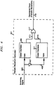
- a typical communication system such as that depicted in FIG. 1, comprises a transmitter 101 which sends information bearing signals over a communications channel 103 to a receiver 105.
- digital signals are transmitted sequentially: each being sent for a constant amount of time and during a precisely defined interval of time.
- the time interval is defined for the transmitter by an electronic metronome known to those skilled in the art as a "clock signal" (hereinafter “clock”).
- a clock is typically generated by a crystal oscillator and is embodied as electric squarewave signal with constant frequency and a 50% duty cycle.
- FIG. 2 at 201 shows a waveform illustrative of a clock.
- FIG. 2 at 207 shows a typical waveform for an information bearing signal over time and with respect to clock 201.
- capacitance, inductance and other parasitic effects prohibit the information bearing signal on lead 207 from changing instantaneously from one defined value to another. The signal may assume, therefore, undefined values during the period of transition.
- FIG. 2 at 211 shows a typical transition from a logical "0" to a logical "1" for the illustrative waveform 207.
- the receiver To assure that the receiver correctly interprets the incoming signals, the receiver must selectively read the incoming signals only at instants when the signals have stabilized and not when they are undergoing transition. This requires the receiver to know when the incoming signals are stable and when they are not.
- the receiver also has an electronic metronome, synchronized to the incoming signal which dictates "read now-wait, read now-wait, read now-wait."
- the receiver has information regarding the frequency or frequencies of the transmitter's clock and has a clock with that same frequency. The receiver's clock, however, will, without more, bear no phase relationship to the incoming signal and thus the receiver will have no synchronized metronome to assist it in reading the incoming signal.
- the receiver may advantageously utilize a "clock recovery system".
- FIG. 3 shows how a clock recovery system may be used in a receiver to correctly read the incoming signal and to extract the transmitted information.
- Incoming signal on lead 301 is fed into clock recovery system 311 to generate a periodic waveform 313 or "recovered clock”.
- the incoming signal 301 is also distributed with optional delay to a data extraction device 307.
- the periodic waveform 313 and the signal 305 are processed in the data extractor 307 to generate the output 309.
- Data extractor 307 could be as simple as a well-known Master/Slave D flip-flop, with signal 305 connected to the D input of the flip-flop, signal 313 connected to the clock input of the flip-flop and output 309 connected to the Q output of the flip-flop.
- the transmitter's clock may be transmitted to the receiver on a communications channel in parallel to the channel carrying the incoming signals.
- the receiver can then estimate the phase of the incoming signals from the phase of the transmitter's clock.
- This technique is disadvantageous in that it requires additional hardware (e.g., the extra communication channel) and is subject to phase skew between the transmitted clock and the incoming signal.
- the phase of the incoming signals may be recovered directly from the incoming signals themselves because the incoming signals carry the information needed to discern its phase. At least two techniques are known which recover the phase of the incoming signals from the incoming signals themselves.
- Open-loop clock recovery system representatively taught by I. Dorros et al., An Experimental 224 Mb/s Digital Repeatered Line, The Bell System Technical Journal, Vol. 45, No. 7, pp. 993-1043 (Sept. 1966).
- Open-loop systems are characterized by a high-Q, narrow bandpass filter (e.g., a SAW filter) yet may be disadvantageous in that they typically require expensive non-integrated components, hundreds of incoming signal transitions to reach steady state and may be susceptible to temperature variations and age.
- the second is the closed-loop clock recovery system.
- a representative closed-loop clock recovery system is taught by R.R. Cordell et al. in A 50 Mhz Phase- and Frequency-Locked Loop , IEEE Journal of Solid State Circuits, Vol. SC-14, No. 6, pp 1003-1010 (Dec. 1979).
- Closed-loop systems are characterized by a phase-locked loop which attempts to lock onto the phase of the incoming signal. While closed-loop recovery systems are self-adjusting (thus mitigating temperature and aging effects) and can be easily integrated, they are disadvantageous in typically requiring hundreds of incoming signal transitions to reach steady state.
- the present invention provides a method and apparatus for recovering the phase of a signal while avoiding many of the costs and restrictions associated with prior apparatus and methods.
- embodiments of the present invention are ideally suited for fabrication on a single integrated circuit and typically generate a "recovered clock" (i.e., recover the phase of an incoming signal) more quickly than methods in the prior art.
- FIG. 1 presents a block diagram of a communication system (prior art).
- FIG. 2 presents a typical clock and data signal as used in a digital communication system (prior art).
- FIG. 3 presents a block diagram of a receiver which incorporates a clock recovery system (prior art).
- FIG. 4 presents an illustrative embodiment of the present invention which utilizes a pair of matched gated oscillators
- FIG. 5 presents an illustrative logic schematic of the embodiment shown in FIG. 4.
- FIG. 6 presents an illustrative transistor schematic corresponding to the logic schematic shown in FIG. 5.
- FIG. 7 presents typical timing diagrams associated with the illustrative embodiment shown in FIG. 4.
- FIG. 8 presents an illustrative embodiment of the present invention utilizing indirect tuning.
- FIG. 9 presents illustrative logical and transistor schematics of a gated variable frequency oscillator useful in the circuit of FIG. 8.
- FIG. 10 presents illustrative logical and transistor schematics of a phase detector useful in the circuit of FIG. 8.
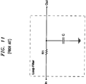
- FIG. 11 presents an illustrative schematic of the loop filter useful in the circuit of FIG. 8.
- FIG. 12 presents an illustrative embodiment of the present invention utilizing direct tuning.
- FIG. 13 presents an illustrative embodiment of the present invention which utilizes a single variable frequency oscillator.
- FIG. 14 presents an illustrative embodiment of the present invention which utilizes a single variable frequency oscillator.
- Phase Bounded Relationship - Two periodic waveforms are said to have a "phase bounded relationship" when the two waveforms have the same frequency and their relative phase stays within a given range.
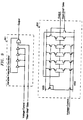
- FIG. 4 of the present application discloses a block diagram of one embodiment of the present invention.
- the embodiment accepts as input an incoming signal on lead 403 which may change states at periodic intervals as defined by a clock, of known frequency, at transmitter 101.
- a typical incoming signal is shown in FIG. 7 at 701.
- the incoming signal on lead 403 is fed into the gate of gated oscillator 405 and into inverter 407.
- the output on lead 413 of gated oscillator 405 is fed into Boolean NOR gate 417.
- the output on lead 409 of inverter 407 is fed into the gate of gated oscillator 411.
- the output on lead 415 of gated oscillator 411 is also fed into Boolean NOR gate 417.
- the output on lead 419 of Boolean NOR gate 417 is the periodic waveform or "recovered clock" n which may be used by the receiver to appropriately read the incoming signal.
- a typical recovered clock corresponding to incoming signal waveform 701 is shown in FIG. 7 at 717.
- a salient characteristic of the illustrative embodiment is the pair of gated oscillators, 405 and 411, each of which is able to generate an oscillatory signal at a given frequency (specifically, the same frequency as the transmitter's clock).
- each gated oscillator outputs no signal when its input is above a first threshold voltage and outputs a periodic waveform when its input is below a second threshold voltage.
- each gated oscillator begins oscillating at the same point in its oscillatory cycle each time its input falls below the second threshold.
- a logic schematic and transistor schematic of an illustrative gated oscillator is shown at 505 and 511 in FIG. 5 and at 605 and 611 in FIG. 6, respectively. Although the transistor schematic in FIG. 6 is shown using CMOS technology, it will be clear to those of ordinary skill in the art how to implement the circuit using other discrete and/or integrated circuit technologies (either electrical or optical).
- the illustrative embodiment in FIG. 4 advantageously also comprises an inverter 407 and a Boolean NOR gate 417.
- a logic schematic and transistor schematic of an illustrative inverter is shown at 507 in FIG. 5 and at 607 in FIG. 6, respectively.
- a logic schematic and transistor schematic of an illustrative Boolean NOR gate is shown at 517 in FIG. 5 and at 617 in FIG. 6, respectively.
- the transistor schematic is shown using CMOS technology, it will be clear to those of ordinary skill in the art how to implement the circuit using other discrete and/or integrated circuit technologies (either electrical or optical).
- the circuit of FIG. 4 operates as follows (see accompanying diagram in FIG. 7).
- gated oscillator 405 does not oscillate and outputs a flat (Boolean logical "0") waveform 713.
- gated oscillator 411 begins oscillation at zero phase and outputs waveform 709.
- the circuit of FIG. 4 is configured in such a way that one and only one of the gated oscillators 405 and 411 is operating to produce a pulse sequence at any one time.
- Each is arranged such that when its input signal level experiences a change from above a first threshold to below a second threshold, it ceases oscillation. Conversely, when the input of each experiences a change from below a third threshold to above a fourth threshold, it immediately begins oscillation at phase zero. Because of inverter 407, it is assumed that only one of gated oscillators 405 and 411 has an input below its activation threshold at any one time.
- gated oscillator 411 When the circuit is powered on (and whenever the incoming signal on lead 403 changes phase) and the incoming signal is below a second threshold, gated oscillator 411 is idle while gated oscillator 405 begins oscillation at zero phase (as shown at 709 and 711, respectively). Whenever a voltage transition (from high to low or low to high) occurs on incoming signal on lead 403, one oscillator becomes idle while the other starts to oscillate at precisely the same point in the oscillatory cycle. As shown in FIG. 7 the respective outputs of gated oscillator 405 and gated oscillator 411 are fed into Boolean NOR gate 417. The output of NOR gate 417 is waveform 717 and may be used extract information from the incoming signal on lead 701. It will be clear to those of ordinary skill in the art how to substitute other logic, including a Boolean NAND gate, for Boolean NOR gate 417.
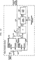
- FIG. 8 discloses a block diagram of one embodiment of the present invention which provides means for tuning oscillators of the type described above.
- the embodiment accepts as input an incoming signal on lead 803 which may change states at periodic intervals as defined by a clock, of known frequency, in transmitter 101.
- the illustrative embodiment shown in FIG. 8 performs as does the illustrative embodiment in FIG. 4.
- the embodiment in FIG. 8 additionally provides for "indirectly" tuning the oscillators with phase-locked loop 841.
- the embodiment of FIG. 8 is advantageous when a semiconductor manufacturer has difficulting in fabricating the embodiment in FIG. 4 within tolerances acceptable to that manufacturer.
- the embodiment of FIG. 8 is advantageously fabricated on a single integrated circuit and, therefore, may be less finicky to manufacturing tolerances than the embodiment in FIG. 8.
- the incoming signal on lead 803 is fed into the gate of gated variable frequency oscillator 805 (henceforth "GVFO") and into inverter 807.
- the output on lead 813 of GVFO 805 is fed into Boolean NOR gate 817.
- the output on lead 809 of inverter 807 is fed into the gate input of GVFO 811.
- the output on lead 815 of GVFO 811 is also fed into Boolean NOR gate 817.
- the output on lead 819 of Boolean NOR gate 817 is the periodic waveform or "recovered clock" which may be used by the receiver to appropriately read the incoming signal.
- a typical recovered clock corresponding to incoming signal on lead 803 is shown in FIG. 7 at 717.
- phase-locked loop 841 receives a reference periodic waveform 831 and sends a tuning signal on lead 830 into the respective control inputs of GVFO 805 and GVFO 811.
- phase-locked loop 841 comprises GVFO 823, counter 825 (optional), phase detector 827 and loop filter 829.
- the design and operation of phase-locked loops is well known to those of ordinary skill in the art.
- a salient characteristic of the illustrative embodiment is the triplet of GVFOs, 805, 811 and 823, each of which is capable of being tuned to oscillate at a given frequency (specifically, the same frequency as the transmitter's clock).
- a signal fed into each GFVO's "control" inputs directs the frequency at which the GFO should oscillate.
- each GVFOs outputs no signal when its respective input is above a first threshold voltage and outputs a periodic waveform when its respective input is below a second threshold voltage.
- each GVFO begins oscillating at the same point in its oscillatory cycle each time its input falls below the second threshold.
- each GVFO has precisely the same electrical and physical characteristics.
- the gate input of GVFO 823 is advantageously tied to ground in order to assure that it continuously oscillates.
- a logic schematic and transistor schematic of an illustrative GVFO is shown at 901 and 903 in FIG. 9. Although the transistor schematic is shown using CMOS technology, it will be clear to those of ordinary skill in the art how to implement the circuit using other discrete and/or integrated circuit technologies (either electrical or optical).
- a logic schematic and transistor schematic of an illustrative phase detector (as shown at 827 in FIG. 8) is shown at 1001 and 1003 in FIG. 10. It will be clear to those of ordinary skill in the art how to implement phase detectors using other discrete and/or integrated circuit technologies (either electrical or optical).
- a schematic of an illustrative loop filter (as shown at 829 in FIG. 8) in FIG. 11.
- the loop filter should be designed so that, so far as is possible, only the DC component of the signal should pass unattenuated and all frequencies above DC should be attenuated as much as possible. It will be clear to those of ordinary skill in the art how to implement phase detectors using other discrete and/or integrated circuit technologies (both electrical and optical).
- the illustrative embodiment in FIG. 8 advantageously also comprises an inverter 807 and a Boolean NOR gate 817.
- a logic schematic and transistor schematic of an illustrative inverter is shown at 505 in FIG. 5 and FIG. 6, respectively.
- a logic schematic and transistor schematic of an illustrative Boolean NOR gate is shown at 507 in FIG. 5 and FIG. 6, respectively.
- the transistor schematic is shown using CMOS technology, it will be clear to those of ordinary skill in the art how to implement the circuit using other discrete and/or integrated circuit technologies (both electrical and optical). It will be clear to those of ordinary skill in the art how to design alternate circuitry which accomplishes the same functionality as that taught here.
- phase-locked loop 841 continuously tunes GVFO 805 and GVFO 811 to oscillate at a frequency determined by reference periodic waveform 831. It should be noted that there is no feedback from GVFO 805 or GVFO 811 into phase-locked loop 841. Thus, phase-locked loop 841 tunes GVFO 805 and GVFO 811 based on the assumption that the electrical and physical characteristics affecting the operation of GVFO 823 within phase-locked loop 841 are virtually identical to those affecting GVFO 805 and GVFO 811. It is therefore advantageous to fabricate GVFO 805, 811 and 823 on a single integrated circuit and with each having virtually identical physical and electrical characteristics (e.g., layouts, voltages).
- the circuit of FIG. 8 operates as follows. When the circuit is powered on (and whenever the incoming signal on lead 803 changes phase) and the incoming signal voltage is above a first threshold, GVFO 805 does not oscillate and outputs a flat (Boolean logical "0") waveform 713. In such a circumstance, however, GVFO 811 begins oscillation at zero phase and outputs waveform 709.
- the circuit of FIG. 8 is configured in such a way that one and only one of the GVFO 405 and 411 is operating to produce a pulse sequence at any one time.
- Each is arranged such that when its input signal level experiences a change from above a first threshold to below a second threshold, it ceases oscillation. Conversely, when the input of each experiences a change from below a third threshold to above a fourth threshold, it immediately begins oscillation at phase zero. Because of inverter 807, it is assumed that only one of GVFO 805 and 811 has an input below its activation threshold at any one time.
- GVFO 811 When the circuit is powered on (and whenever the incoming signal on lead 803 changes phase) and the incoming signal is below a second threshold, GVFO 811 is idle while GVFO 805 begins oscillation at zero phase (as shown at 709 and 711, respectively). Whenever a voltage transition (from high to low or low to high) occurs on incoming signal on lead 803, one oscillator becomes idle while the other starts to oscillate at precisely the same point in the oscillatory cycle. As shown in FIG. 7 the respective outputs of gated oscillator 805 and GVFO 811 are fed into Boolean NOR gate 817. The output of NOR gate 817 is waveform 717 and may be used extract information from the incoming signal on lead 701. It will be clear to those of ordinary skill in the art how to substitute other logic, including a Boolean NAND gate, for Boolean NOR gate 817.
- FIG. 12 discloses a block diagram of one embodiment of the present invention which provides means for tuning oscillators of the type described above.
- the embodiment accepts as input an incoming signal on lead 1203 which may change states at periodic intervals as defined by a clock, of known frequency, in transmitter 101.
- the illustrative embodiment shown in FIG. 12 performs as does the illustrative embodiment in FIG. 4 and FIG. 8.
- the embodiment in FIG. 12 additionally provides for "directly" tuning the oscillators with phase-locked loop 841 which utilizes the recovered clock 1219.
- the embodiment of FIG. 12 is advantageous when a semiconductor manufacturer has difficulting in fabricating the embodiment in FIG. 4 within tolerances acceptable to that manufacturer.
- the embodiment of FIG. 8 is advantageously fabricated on a single integrated circuit but need not be.
- FIG. 13 discloses a block diagram of one embodiment of the present invention which provides means for tuning oscillators of the type described above.
- the embodiment accepts as input an incoming signal which may change states at periodic intervals as defined by a clock, of known frequency, in transmitter 101.
- the embodiment depicted in FIG. 13 uses edge detectors 1301 and 1305 and Boolean NOR gate to turn GVFO 1315 alternately ON and OFF.
- the embodiment in FIG. 13 can be fabricated with means 1321 for tuning GVFO 1315 or not depending on the particular application. Utilization of means for tuning (e.g., a phase-locked loop) will advantageously improve the precision of the recovered clock.
- means for tuning e.g., a phase-locked loop
- FIG. 14 discloses a block diagram of one embodiment of the present invention which provides means for tuning oscillators of the type described above.
- the embodiment accepts as input an incoming signal which may change states at periodic intervals as defined by a clock, of known frequency, in transmitter 101.
- the embodiment depicted in FIG. 14 uses edge detectors 1401 and 1405, Boolean NOR gate 1411 and one-shot 1415 to turn GVFO 1419 alternately ON and OFF.
- the embodiment in FIG. 14 can be fabricated with means 1423 for tuning GVFO 1419 or not depending on the particular application. Utilization of means for tuning (e.g., a phase-locked loop) will advantageously improve the precision of the recovered clock.
- means for tuning e.g., a phase-locked loop
Applications Claiming Priority (2)
| Application Number | Priority Date | Filing Date | Title |
|---|---|---|---|
| US880428 | 1992-05-08 | ||
| US07/880,428 US5237290A (en) | 1992-05-08 | 1992-05-08 | Method and apparatus for clock recovery |
Publications (2)
| Publication Number | Publication Date |
|---|---|
| EP0569179A2 true EP0569179A2 (fr) | 1993-11-10 |
| EP0569179A3 EP0569179A3 (en) | 1994-06-01 |
Family
ID=25376264
Family Applications (1)
| Application Number | Title | Priority Date | Filing Date |
|---|---|---|---|
| EP19930303233 Withdrawn EP0569179A3 (en) | 1992-05-08 | 1993-04-26 | A method and apparatus for clock recovery |
Country Status (4)
| Country | Link |
|---|---|
| US (1) | US5237290A (fr) |
| EP (1) | EP0569179A3 (fr) |
| JP (1) | JPH0653950A (fr) |
| KR (1) | KR930022718A (fr) |
Cited By (3)
| Publication number | Priority date | Publication date | Assignee | Title |
|---|---|---|---|---|
| EP0666662A1 (fr) * | 1994-02-07 | 1995-08-09 | Motorola, Inc. | Récepteur d'horloge de données en série et méthode correspondante |
| EP0903885A2 (fr) * | 1997-09-18 | 1999-03-24 | Nec Corporation | Circuit de récupération d'horloge |
| US7667544B2 (en) | 2006-01-12 | 2010-02-23 | Yokogawa Electric Corporation | Clock reproducing apparatus |
Families Citing this family (29)
| Publication number | Priority date | Publication date | Assignee | Title |
|---|---|---|---|---|
| US5646562A (en) * | 1993-07-21 | 1997-07-08 | Seiko Epson Corporation | Phase synchronization circuit, one-shot pulse generating circuit and signal processing system |
| US5834980A (en) * | 1994-01-03 | 1998-11-10 | Lucent Technologies Inc. | Method and apparatus for supplying synchronization signals securing as clock signals with defined phase relationships |
| US5541961A (en) * | 1994-08-15 | 1996-07-30 | At&T Corp. | Digitally controlled high resolution hybrid phase synthesizer |
| US5675620A (en) * | 1994-10-26 | 1997-10-07 | At&T Global Information Solutions Company | High-frequency phase locked loop circuit |
| US5757872A (en) * | 1994-11-30 | 1998-05-26 | Lucent Technologies Inc. | Clock recovery circuit |
| US6239843B1 (en) * | 1997-05-05 | 2001-05-29 | Wavo Corporation | Method and system for decoding data in a signal |
| US6018273A (en) * | 1997-10-15 | 2000-01-25 | Zilog, Inc. | Externally-synchronized voltage-controlled oscillator in phase locked loop |
| US6166606A (en) * | 1999-02-10 | 2000-12-26 | Zilog, Inc. | Phase and frequency locked clock generator |
| KR100416512B1 (ko) | 1999-06-15 | 2004-01-31 | 샤프 가부시키가이샤 | 비트동기회로 |
| US6850580B1 (en) | 1999-06-21 | 2005-02-01 | Sharp Kabushiki Kaisha | Bit synchronizing circuit |
| US6259326B1 (en) | 1999-08-24 | 2001-07-10 | Agere Systems Guardian Corp. | Clock recovery from a burst-mode digital signal each packet of which may have one of several predefined frequencies |
| US6570694B1 (en) | 2000-03-03 | 2003-05-27 | Alcatel | System and method for low-jitter asynchronous optical regeneration using wavelength sampling |
| TW496035B (en) * | 2000-04-25 | 2002-07-21 | Univ Singapore | Method and apparatus for a digital clock multiplication circuit |
| US7010077B1 (en) | 2000-11-20 | 2006-03-07 | Agere Systems Inc. | Gated clock recovery circuit |
| US6552619B2 (en) | 2001-02-05 | 2003-04-22 | Pmc Sierra, Inc. | Multi-channel clock recovery circuit |
| JP4158465B2 (ja) * | 2002-09-10 | 2008-10-01 | 日本電気株式会社 | クロック再生装置、および、クロック再生装置を用いた電子機器 |
| KR100467322B1 (ko) | 2002-09-18 | 2005-01-24 | 한국전자통신연구원 | 버스트 모드 클럭신호 재생장치 및 방법 |
| US7123675B2 (en) * | 2002-09-25 | 2006-10-17 | Lucent Technologies Inc. | Clock, data and time recovery using bit-resolved timing registers |
| US6889441B2 (en) * | 2003-09-17 | 2005-05-10 | Seiffert Industrial Sales Company | Laser roller alignment system |
| TWI242929B (en) * | 2004-12-01 | 2005-11-01 | Ind Tech Res Inst | Clock and data recovery apparatus and method thereof |
| TWI277302B (en) * | 2004-12-28 | 2007-03-21 | Ind Tech Res Inst | Clock and data recovery circuit |
| US7542533B2 (en) * | 2005-07-07 | 2009-06-02 | Agere Systems Inc. | Apparatus and method for calibrating the frequency of a clock and data recovery circuit |
| KR100656370B1 (ko) * | 2005-12-05 | 2006-12-11 | 한국전자통신연구원 | 위상 보간 클럭을 이용한 데이터 복원 장치 및 방법 |
| US8243869B2 (en) * | 2006-11-28 | 2012-08-14 | Broadlight Ltd. | Burst mode clock and data recovery circuit and method |
| JP5103940B2 (ja) * | 2007-02-28 | 2012-12-19 | 横河電機株式会社 | クロック再生装置 |
| US7786814B2 (en) * | 2008-08-28 | 2010-08-31 | Agere Systems Inc. | Method and apparatus for deriving an integrated circuit (IC) clock with a frequency offset from an IC system clock |
| JP5397025B2 (ja) * | 2009-06-02 | 2014-01-22 | ソニー株式会社 | クロック再生装置および電子機器 |
| US8922150B1 (en) * | 2012-07-18 | 2014-12-30 | The Johns Hopkins University | Differential serial driver |
| JP6032082B2 (ja) * | 2013-03-25 | 2016-11-24 | 富士通株式会社 | 受信回路及び半導体集積回路 |
Citations (5)
| Publication number | Priority date | Publication date | Assignee | Title |
|---|---|---|---|---|
| JPS5954344A (ja) * | 1982-09-22 | 1984-03-29 | Fuji Electric Co Ltd | タイミング再生装置 |
| WO1985000941A1 (fr) * | 1983-08-05 | 1985-02-28 | Advanced Micro Devices, Inc. | Oscillateur a interruptions commande en tension |
| US4523158A (en) * | 1983-02-02 | 1985-06-11 | Rca Corporation | Clock regenerator using two on-off oscillators |
| EP0307595A1 (fr) * | 1987-09-11 | 1989-03-22 | Siemens Aktiengesellschaft | Montage de circuit pour la génération de deux fréquences très proches |
| US5068628A (en) * | 1990-11-13 | 1991-11-26 | Level One Communications, Inc. | Digitally controlled timing recovery loop |
Family Cites Families (4)
| Publication number | Priority date | Publication date | Assignee | Title |
|---|---|---|---|---|
| US3893042A (en) * | 1973-12-12 | 1975-07-01 | Us Navy | Lock indicator for phase-locked loops |
| US4567448A (en) * | 1982-08-05 | 1986-01-28 | Epson Corporation | Variable frequency oscillator |
| JPH0620197B2 (ja) * | 1987-09-09 | 1994-03-16 | 日本電気株式会社 | 速度可変型クロック再生回路 |
| US5134637A (en) * | 1991-03-22 | 1992-07-28 | Motorola, Inc. | Clock recovery enhancement circuit |
-
1992
- 1992-05-08 US US07/880,428 patent/US5237290A/en not_active Expired - Fee Related
-
1993
- 1993-04-26 EP EP19930303233 patent/EP0569179A3/en not_active Withdrawn
- 1993-04-27 KR KR1019930007058A patent/KR930022718A/ko not_active Application Discontinuation
- 1993-05-07 JP JP5130096A patent/JPH0653950A/ja active Pending
Patent Citations (5)
| Publication number | Priority date | Publication date | Assignee | Title |
|---|---|---|---|---|
| JPS5954344A (ja) * | 1982-09-22 | 1984-03-29 | Fuji Electric Co Ltd | タイミング再生装置 |
| US4523158A (en) * | 1983-02-02 | 1985-06-11 | Rca Corporation | Clock regenerator using two on-off oscillators |
| WO1985000941A1 (fr) * | 1983-08-05 | 1985-02-28 | Advanced Micro Devices, Inc. | Oscillateur a interruptions commande en tension |
| EP0307595A1 (fr) * | 1987-09-11 | 1989-03-22 | Siemens Aktiengesellschaft | Montage de circuit pour la génération de deux fréquences très proches |
| US5068628A (en) * | 1990-11-13 | 1991-11-26 | Level One Communications, Inc. | Digitally controlled timing recovery loop |
Non-Patent Citations (1)
| Title |
|---|
| PATENT ABSTRACTS OF JAPAN vol. 8, no. 149 (E-255)12 July 1984 & JP-A-59 054 344 (FUJI DENKI SEIZO KK) 29 March 1984 * |
Cited By (4)
| Publication number | Priority date | Publication date | Assignee | Title |
|---|---|---|---|---|
| EP0666662A1 (fr) * | 1994-02-07 | 1995-08-09 | Motorola, Inc. | Récepteur d'horloge de données en série et méthode correspondante |
| EP0903885A2 (fr) * | 1997-09-18 | 1999-03-24 | Nec Corporation | Circuit de récupération d'horloge |
| EP0903885A3 (fr) * | 1997-09-18 | 2003-05-28 | NEC Electronics Corporation | Circuit de récupération d'horloge |
| US7667544B2 (en) | 2006-01-12 | 2010-02-23 | Yokogawa Electric Corporation | Clock reproducing apparatus |
Also Published As
| Publication number | Publication date |
|---|---|
| KR930022718A (ko) | 1993-11-24 |
| JPH0653950A (ja) | 1994-02-25 |
| EP0569179A3 (en) | 1994-06-01 |
| US5237290A (en) | 1993-08-17 |
Similar Documents
| Publication | Publication Date | Title |
|---|---|---|
| US5237290A (en) | Method and apparatus for clock recovery | |
| KR940001724B1 (ko) | 위상동기회로 | |
| US8537954B2 (en) | Method and apparatus for multi-mode clock data recovery | |
| AU618202B2 (en) | Phase locked loop circuit with digital control | |
| US5285483A (en) | Phase synchronization circuit | |
| US5399995A (en) | CMOS circuit providing 90 degree phase delay | |
| EP1143606B1 (fr) | Oscillateur variable commandé numériquement | |
| US6259326B1 (en) | Clock recovery from a burst-mode digital signal each packet of which may have one of several predefined frequencies | |
| US5581216A (en) | Low jitter voltage controlled oscillator (VCO) circuit | |
| US6900675B2 (en) | All digital PLL trimming circuit | |
| US5276716A (en) | Bi-phase decoder phase-lock loop in CMOS | |
| US6873669B2 (en) | Clock signal reproduction device | |
| US5666388A (en) | Clock recovery circuit with matched oscillators | |
| US5343169A (en) | Frequency locked loop | |
| EP0287776B1 (fr) | Détecteur de données à verrouillage de phase | |
| JP3346445B2 (ja) | 識別・タイミング抽出回路 | |
| KR20000077201A (ko) | 두 위상의 디지털 위상 동기 루프 회로 | |
| KR100430618B1 (ko) | 피엘엘 회로 | |
| US6188739B1 (en) | Modified third order phase-locked loop | |
| JP2004515957A (ja) | データ信号からクロック信号を回復するための位相同期ループ | |
| JP2008541685A (ja) | 到達時間同期ループ | |
| KR100280452B1 (ko) | 위상동기루프장치 | |
| EP0480597B1 (fr) | Dispositif de boucle à verrouillage de phase | |
| KR100852570B1 (ko) | 클록 복원 회로 및 클록 신호 복원 방법 | |
| JP3473413B2 (ja) | 位相同期回路 |
Legal Events
| Date | Code | Title | Description |
|---|---|---|---|
| PUAI | Public reference made under article 153(3) epc to a published international application that has entered the european phase |
Free format text: ORIGINAL CODE: 0009012 |
|
| AK | Designated contracting states |
Kind code of ref document: A2 Designated state(s): DE FR GB IT |
|
| PUAL | Search report despatched |
Free format text: ORIGINAL CODE: 0009013 |
|
| AK | Designated contracting states |
Kind code of ref document: A3 Designated state(s): DE FR GB IT |
|
| RAP3 | Party data changed (applicant data changed or rights of an application transferred) |
Owner name: AT&T CORP. |
|
| 17P | Request for examination filed |
Effective date: 19941116 |
|
| 17Q | First examination report despatched |
Effective date: 19960705 |
|
| STAA | Information on the status of an ep patent application or granted ep patent |
Free format text: STATUS: THE APPLICATION IS DEEMED TO BE WITHDRAWN |
|
| 18D | Application deemed to be withdrawn |
Effective date: 19980715 |