EP0555858B1 - Trockenätzverfahren eines Polyzids ohne Verwendung von FCKW-Gasen - Google Patents
Trockenätzverfahren eines Polyzids ohne Verwendung von FCKW-Gasen Download PDFInfo
- Publication number
- EP0555858B1 EP0555858B1 EP93102170A EP93102170A EP0555858B1 EP 0555858 B1 EP0555858 B1 EP 0555858B1 EP 93102170 A EP93102170 A EP 93102170A EP 93102170 A EP93102170 A EP 93102170A EP 0555858 B1 EP0555858 B1 EP 0555858B1
- Authority
- EP
- European Patent Office
- Prior art keywords
- etching
- dry etching
- sulfur
- etching method
- silicide layer
- Prior art date
- Legal status (The legal status is an assumption and is not a legal conclusion. Google has not performed a legal analysis and makes no representation as to the accuracy of the status listed.)
- Expired - Lifetime
Links
Images

Classifications
-
- H—ELECTRICITY
- H01—ELECTRIC ELEMENTS
- H01L—SEMICONDUCTOR DEVICES NOT COVERED BY CLASS H10
- H01L21/00—Processes or apparatus adapted for the manufacture or treatment of semiconductor or solid state devices or of parts thereof
- H01L21/02—Manufacture or treatment of semiconductor devices or of parts thereof
- H01L21/04—Manufacture or treatment of semiconductor devices or of parts thereof the devices having at least one potential-jump barrier or surface barrier, e.g. PN junction, depletion layer or carrier concentration layer
- H01L21/18—Manufacture or treatment of semiconductor devices or of parts thereof the devices having at least one potential-jump barrier or surface barrier, e.g. PN junction, depletion layer or carrier concentration layer the devices having semiconductor bodies comprising elements of Group IV of the Periodic System or AIIIBV compounds with or without impurities, e.g. doping materials
- H01L21/30—Treatment of semiconductor bodies using processes or apparatus not provided for in groups H01L21/20 - H01L21/26
- H01L21/302—Treatment of semiconductor bodies using processes or apparatus not provided for in groups H01L21/20 - H01L21/26 to change their surface-physical characteristics or shape, e.g. etching, polishing, cutting
-
- H—ELECTRICITY
- H01—ELECTRIC ELEMENTS
- H01L—SEMICONDUCTOR DEVICES NOT COVERED BY CLASS H10
- H01L21/00—Processes or apparatus adapted for the manufacture or treatment of semiconductor or solid state devices or of parts thereof
- H01L21/02—Manufacture or treatment of semiconductor devices or of parts thereof
- H01L21/04—Manufacture or treatment of semiconductor devices or of parts thereof the devices having at least one potential-jump barrier or surface barrier, e.g. PN junction, depletion layer or carrier concentration layer
- H01L21/18—Manufacture or treatment of semiconductor devices or of parts thereof the devices having at least one potential-jump barrier or surface barrier, e.g. PN junction, depletion layer or carrier concentration layer the devices having semiconductor bodies comprising elements of Group IV of the Periodic System or AIIIBV compounds with or without impurities, e.g. doping materials
- H01L21/30—Treatment of semiconductor bodies using processes or apparatus not provided for in groups H01L21/20 - H01L21/26
- H01L21/31—Treatment of semiconductor bodies using processes or apparatus not provided for in groups H01L21/20 - H01L21/26 to form insulating layers thereon, e.g. for masking or by using photolithographic techniques; After treatment of these layers; Selection of materials for these layers
- H01L21/3205—Deposition of non-insulating-, e.g. conductive- or resistive-, layers on insulating layers; After-treatment of these layers
- H01L21/321—After treatment
- H01L21/3213—Physical or chemical etching of the layers, e.g. to produce a patterned layer from a pre-deposited extensive layer
- H01L21/32133—Physical or chemical etching of the layers, e.g. to produce a patterned layer from a pre-deposited extensive layer by chemical means only
- H01L21/32135—Physical or chemical etching of the layers, e.g. to produce a patterned layer from a pre-deposited extensive layer by chemical means only by vapour etching only
- H01L21/32136—Physical or chemical etching of the layers, e.g. to produce a patterned layer from a pre-deposited extensive layer by chemical means only by vapour etching only using plasmas
- H01L21/32137—Physical or chemical etching of the layers, e.g. to produce a patterned layer from a pre-deposited extensive layer by chemical means only by vapour etching only using plasmas of silicon-containing layers
-
- H—ELECTRICITY
- H01—ELECTRIC ELEMENTS
- H01L—SEMICONDUCTOR DEVICES NOT COVERED BY CLASS H10
- H01L21/00—Processes or apparatus adapted for the manufacture or treatment of semiconductor or solid state devices or of parts thereof
- H01L21/02—Manufacture or treatment of semiconductor devices or of parts thereof
- H01L21/04—Manufacture or treatment of semiconductor devices or of parts thereof the devices having at least one potential-jump barrier or surface barrier, e.g. PN junction, depletion layer or carrier concentration layer
- H01L21/18—Manufacture or treatment of semiconductor devices or of parts thereof the devices having at least one potential-jump barrier or surface barrier, e.g. PN junction, depletion layer or carrier concentration layer the devices having semiconductor bodies comprising elements of Group IV of the Periodic System or AIIIBV compounds with or without impurities, e.g. doping materials
- H01L21/30—Treatment of semiconductor bodies using processes or apparatus not provided for in groups H01L21/20 - H01L21/26
- H01L21/31—Treatment of semiconductor bodies using processes or apparatus not provided for in groups H01L21/20 - H01L21/26 to form insulating layers thereon, e.g. for masking or by using photolithographic techniques; After treatment of these layers; Selection of materials for these layers
- H01L21/3205—Deposition of non-insulating-, e.g. conductive- or resistive-, layers on insulating layers; After-treatment of these layers
- H01L21/321—After treatment
- H01L21/3213—Physical or chemical etching of the layers, e.g. to produce a patterned layer from a pre-deposited extensive layer
- H01L21/32139—Physical or chemical etching of the layers, e.g. to produce a patterned layer from a pre-deposited extensive layer using masks
Definitions
- This invention relates to a dry etching method employed in such applications as production of semiconductor devices, and more particularly to a dry etching method for etching a polycide film whereby high selectivity, high anisotropy and low pollution can be achieved without using a chlorofluorocarbon (CFC) gas.
- CFC chlorofluorocarbon
- a polycide film formed by stacking a polysilicon layer and a refractory metal silicide layer composed of a tungsten silicide or WSi x , for example, has been used broadly for recent years as a gate metallization material for LSI, because the polycide film exhibits resistance smaller than a single-layer film of a polysilicon by one order of magnitude for an identical cross-sectional area.
- the polycide film Since anisotropy should be realized for two different materials, the polycide film has brought about a new type of difficulty to the dry etching technique. That is, defects such as undercuts and constrictions tend to be generated on a pattern, because the lower layer or the polysilicon layer is etched faster than the upper layer or the refractory metal silicide layer due to the difference in vapor pressure of a resultant halogen compound, and because a reaction layer is formed on the boundary surface between the polysilicon layer and the refractory metal silicide layer.
- a chlorofluorocarbon or CFC gas typified by CFC-113 (C 2 Cl 3 F 3 ) has been used broadly as an etching gas for the polycide film for the following reasons.
- F and Cl atoms in each molecule promote both a radical reaction and an ion assisted reaction, and deposited carbonaceous polymers perform sidewall protection, thereby making it possible to carry out anisotropic etching with a high etchrate.
- the present applicant proposed, in the Japanese patent gazette, KOKAI TOKKYO KOHO No.3-215938, a two-stage etching technique for etching a WSi x layer on the upper side of a tungsten polycide film, referred to as a W-polycide film hereinafter, by using HBr/SF 6 mixed gas, while etching a polysilicon layer on the lower side by using HBr gas alone.
- This technique has significant advantages such as capability of achieving a practical etchrate, high anisotropy and high selectivity for a gate oxide film while preventing particle pollution due to WBr x or tungsten bromide.
- CFC-free measure is a method of etching a W-polycide film by using Cl 2 /CH 2 F 2 mixed gas instead of CFC-113, which is reported in the Extended Abstract of the 52nd Fall Meeting of the Japan Society of Applied Physics and Related Societies, 1991, p.508, 9a-ZF-6.
- sidewall protection is performed by depositing carbonaceous polymers formed in the gaseous phase from CH 2 F 2 . Also, if the flow rate of CH 2 F 2 is optimized, selectivity between the WSi x layer and the polysilicon layer can be increased, and residues on steps can be reduced.
- practicality of the two-stage etching technique by using a HBr/SF 6 mixed gas and a single HBr gas depends upon how precisely the timing for a change of gas composition between the WSi x layer and the polysilicon layer can be decided. If the timing for the change is too early, the remaining WSi x layer reacts with the single-composition HBr gas thereby forming WBr x of low vapor pressure, and therefore, deterioration of the particle level is very likely to take place. On the contrary, if the timing for the change is delayed, undercuts will be generated on the polysilicon layer by F*.
- the method using the Cl 2 /CH 2 F 2 mixed gas has a problem of excessive deposition of CH 2 F 2 . It is reported in the Extended Abstract of the Dry Process Symposium, 1988, p.74, II-8, that a CH 2 F 2 gas forms relatively rigid polymers compared with C 4 F 8 , C 2 Cl 2 F 4 (CFC-114), and CCl 4 gases, has a low etchrate by incident ions. Accordingly, the use of CH 2 F 2 is likely to deteriorate reproducibility and the particle level.
- a low-temperature etching is expected to be one of promising CFC-free etching methods.
- this method attempts to achieve high anisotropy only by freezing or inhibiting a radical reaction, a substrate to be etched (wafer) needs to be cooled to such a degree as to require liquid nitrogen.
- hardware related problems arise, such as increased demand for large-scale special cooling equipment and decreased reliability of vacuum sealant. Also anticipated is that additional time taken to cool the wafer below a room temperature and heat it back to the room temperature leads to a reduction in throughput as well as economy and productivity.
- EP-A-0 517 165 - representing prior art according to Art. 54(3), (4) EPC for all contracting states designated in the present application and to the extent of the content of its priority documents JP 15479/91 and JP 290492/91 - discloses a dry etching method using etching gas containing a sulfur based compound capable of forming free sulfur in a plasma while dissociated by electric discharges.
- the wafers are cooled to temperatures of - 50 °C to 0 °C during the etching of the polycide films (examples 1 to 4).
- EP-A-0 498 209 - representing prior art according to Art. 54(3), (4) EPC for all contracting states designated in the present application - discloses a method for dry etching silicon based material without using a chlorofluorocarbon gas. In this method, etching is performed with an etching gas comprising a sulfur halide on wafers having a temperature between - 70 °C and - 30 °C.
- the object of the present invention is to provide a practical dry etching method for etching a polycide film whereby such problems as difficulty in deciding the timing for a change in the two-stage etching, pollution due to carbonaceous polymers and a decline in selectivity, and troubles caused by low-temperature control of the wafer can be solved.
- the points or effects of the dry etching method of the present invention are as follows: 1) fluorine based compounds are not used as components of the etching gas; 2) sidewall protection is performed with substances other than carbonaceous polymers; and 3) one-stage etching is realized without changing etching conditions during the process.
- Cl* and/or Br* are used for etching instead of F*, which causes a decline in anisotropy.
- Cl* and Br* are not positively used because of low vapor pressure of chlorides and bromides of W.
- the boiling points of WCl 5 , WCl 6 and WBr 6 are 275.6°C, 346.7°C and 232°C, respectively, and these boiling points are higher than that of WF 6 , which is in a gaseous state at a normal temperature.
- S may be formed by using a compound which can release free S in a plasma when dissociated by electric discharges, as reported in the Monthly Journal "Semiconductor World,” published by the Press Journal Inc., January 1993, p.140-144.
- the deposited S can be removed through sublimation if the etched wafer is heated to approximately 90°C or above.
- Sulfur nitride based compounds can be formed in a similar manner if a nitrogen based compound is added to a compound which can produce S, as proposed by the present inventor before.
- the sulfur nitride compound formed in this process is mainly polythiazyl (SN) x , and the following description centers on (SN) x .
- SN polythiazyl
- thiazyl halide and hydrogen thiazyl other than (SN) x may be formed in accordance with composition of etching gas, all these compounds can be easily removed through sublimation or decomposition if the wafer is heated to approximately 130°C or above.
- the wafer is heated on the assumption of such a temperature range that these S and sulfur nitride based compounds cannot be removed.
- the sulfur deposition process can be realized by using at least one of compounds which can simultaneously supply S and Cl*, or S and Br*, from one molecule as a main component of tne etching gas.
- compounds which can simultaneously supply S and Cl*, or S and Br*, from one molecule as a main component of tne etching gas.
- Typical of such compounds are sulfur chlorides, for instance, S 3 Cl 2 , S 2 Cl 2 and SCl 2 , or sulfur bromides such as S 3 Br 2 , S 2 Br 2 and SBr 2 .
- Cl* and Br* contribute to etching of the polycide film as etchants, and S as a sidewall protection substance.
- the sulfur nitride deposition process can be realized by further adding a nitrogen based compound to the etching gas containing at least either sulfur chlorides or sulfur bromides.
- a nitrogen based compound containing at least either sulfur chlorides or sulfur bromides.
- S formed through dissociation from sulfur chlorides and/or sulfur bromides and N formed through dissociation from nitrogen based compounds react with each other, thiazyl (N ⁇ S) is formed first, and then the formed thiazyl performs nucleophilic attack by using unpaired electrons, so that the molecules easily polymerize to form (SN) 2 , (SN) 4 and furthermore, polythiazyl (SN) x .
- (SN) x in a crystalline state has a structure wherein covalent bond chains, S-N-S-N- ⁇ , are arranged in parallel with each other, as described in J. Am. Chem. Soc., Vol.29, 1975, p.6358-6363.
- This polymer exhibits high resistance to the attack of radicals and ions, and therefore, demonstrates stronger sidewall protection effects than sulfur.
- the above-mentioned S 2 Cl 2 (disulfur dichloride) has a melting point of -77°C and a boiling point of 138°C
- the S 2 Br 2 (disulfur dibromide) has a melting point of -46°C and a boiling point of 54°C (2.39 ⁇ 10 3 Pa), both of which are liquid or oily substances at a normal temperature and under normal pressure.
- these substances can be used as etching gas even with single composition.
- liquid sulfur halide is limited to the two above-mentioned substances as a matter of convenience.
- sulfur halide there are many compounds having other atomic composition ratios with uncertain presence and characteristics in a pure state. Theoretically, it is possible to obtain similar mixed gas products even by using these uncertain compounds.
- selectivity for resist improves by supplying BCl 3 and BBr 3 mixed in advance, in etching an aluminum based material layer.
- the present invention is based on this fact. Although detailed mechanism of this improvement in selectivity is not made clear, it is considered that high resistance to sputtering operation of ions and attacks of radicals can be given by complicating and diversifying the structure and properties of a CCl x Br y based polymer formed on the surface of a resist mask.
- the one-stage etching for the polycide film which was conventionally difficult is realized without using a CFC gas.
- controllability of etching can be significantly improved.
- the etching gas contains no carbon, selectivity for the SiO 2 based underlying layer can be improved, and particle pollution can be prevented.
- the present invention is highly suitable for production of semiconductor devices demanding high integration, high performance and high reliability, and is designed on the basis of minute rules.
- a method according to the present invention is applied to a gate electrode forming process wherein a W-polycide film was etched by using a S 2 Cl 2 gas.
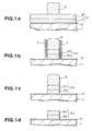
- the process is described by referring to Figs.1a to 1d.
- a wafer was prepared, being composed of a W-polycide film 5 formed on a single-crystal silicon substrate 1 via a gate oxide film 2, and a resist mask 6 patterned in a predetermined shape and formed thereon, as shown in Fig.1a.
- the W-polycide film 5 was composed of a polysilicon layer 3 and a WSi x layer 4 stacked in this order, the polysilicon layer 3 having a thickness of about 100 nm with n-type impurities doped therein and the WSi x layer 4 having a thickness of about 100 nm.
- the resist mask 6 was patterned in a width of about 0.35 ⁇ m by performing KrF excimer laser lithography by using, for example, a negative three-component chemical amplification photoresist material, supplied by Shipley Co., Ltd.; product name SAL-601.
- This wafer was set on an RF-biased magnetically enhanced microwave plasma etcher, and the W-polycide film 5 thereon was etched, for instance, under the following conditions: S 2 Cl 2 flow rate 50 SCCM gas pressure 1.3 Pa (10 mTorr) microwave power 850 W (2.45 GHz) RF bias power 50 W (2 MHz) wafer temperature 80°C
- the S 2 Cl 2 which is a liquid substance at a normal temperature, is vaporized by bubbling with an He gas and then introduced into an etching chamber.
- a reaction product WCl x formed in etching the WSi x layer 4 is a compound with a high boiling point. Since the wafer was heated to 80°C in the above-mentioned high vacuum state, the reaction product obtained vapor pressure sufficient for elimination, and therefore generated no particle pollution.
- free S was dissociated from S 2 Cl 2 , and formed sidewall protection films 7, as shown in Fig.1b. With the assistance effects of ions and sidewall protection effects, a gate electrode 5a having a highly anisotropic shape even in one-stage etching was formed.
- a pattern of each material layer formed after etching is indicated by an original number with letter "a" added thereto.
- etching gas did not contain carbon, selectivity of 50 or higher for the gate oxide film 2 was secured, unlike in a conventional process using CFC gas.
- the resist mask 6 was removed by O 2 plasma ashing in accordance with conventional conditions, as shown in Fig.1d. According to this ashing process, remaining small amount of S, if any, can be perfectly removed in the form of SO x .
- the sidewall protection films 7 may be removed simultaneously with the resist mask 6.
- a W-polycide film was etched by using an S 2 Cl 2 /S 2 Br 2 mixed gas.
- a wafer shown in Fig.1a was set on a magnetically enhanced microwave plasma etcher, and a W-polycide film 5 thereon was etched, for instance, under the following conditions: S 2 Cl 2 flow rate 25 SCCM S 2 Br 2 flow rate 25 SCCM gas pressure 1.3 Pa (10 mTorr) microwave power 850 W (2.45 GHz) RF bias power 50 W (2 MHz) wafer temperature 80°C
- a gate electrode 5a having a highly anisotropic shape was formed by one-stage etching.
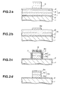
- a patterned TiON layer formed as an antireflection film on a W-polycide film was used as an etching mask, and S 2 Br 2 was used as an etching gas.
- S 2 Br 2 was used as an etching gas. The process is described by referring to Figs.2a to 2d, wherein numerals are partly common to Figs.1a to 1d.
- Fig.2a shows a wafer before etching. Unlike the wafer previously shown in Fig.1a, this wafer is composed of a TiON antireflection film 8 having a thickness of about 40 nm formed on the surface of a W-polycide film 5 by reactive sputtering. Because of the presence of the TiON antireflection film 8, a resist mask 6 is exempt from effects of a strong reflection light from a WSi x layer 4, and is patterned in a highly anisotropic shape.
- the wafer was set on a magnetron RIE apparatus, and the TiON antireflection film 8 was etched, for instance, under the following conditions: c-C 4 F 8 flow rate 30 SCCM O 2 flow rate 20 SCCM gas pressure 1.3 Pa (10 mTorr) microwave power 850 W (2.45 GHz) RF bias power 1000 W (13.56 MHz)
- c-C 4 F 8 (octafluorocyclobutane) is one of so-called fluorocarbon compounds of higher order, and contributes to high-rate etching with assistance of ions by forming a plurality of CF x + from one molecule.
- the TiON antireflection film 8 was removed by this etching in the form of TiO x F y .
- the wafer was moved onto a plasma asher, and the resist mask 6 was removed under the conditions of the conventional O 2 plasma ashing, whereby the TiON antireflection film pattern 8a was formed, as shown in Fig.2b.
- the TiON antireflection film 8 which had been used as the antireflection film was then used as the etching mask.
- the wafer was set on the magnetically enhanced microwave plasma etcher, and the W-polycide film 5 thereon was etched, for instance, under the following conditions: S 2 Br 2 flow rate 50 SCCM gas pressure 1.3 Pa (10 mTorr) microwave power 850 W (2.45 GHz) RF bias power 50 W (2 MHz) wafer temperature 80°C
- the mechanism of etching the W-polycide film 5 in this process is substantially identical to the mechanism in Example 1 with the use of bromine instead of chlorine. With this mechanism of etching, a gate electrode 5a having a highly anisotropic shape was formed, as shown in Fig.2c. Since reaction products WBr x in this case had higher vapor pressure than WCl x , the etchrate improved compared with Example 1.
- Sidewall protection films 7 were formed on pattern sidewalls by depositing S produced through dissociation from S 2 Br 2 .
- TiON antireflection film pattern 8a Ti atoms were extracted by action of Br* in a plasma while a dangling bond of N was formed. This dangling bond is combined with S in the plasma, thereby forming a sulfur nitride based deposition layer 9.
- Fig.2c schematically shows a state of polythiazyl (SN) x deposition.
- the sulfur nitride based deposition layer 9 exhibited high resistance to attacks of incident ions and radicals, and enabled a thin TiON antireflection film pattern 8a to function as the etching mask.
- the sidewall protection films 7 composed of S and the sulfur nitride based deposition layer 9 composed of (SN) x were removed through sublimation or decomposition.
- the etching gas did not contain carbon, and the resist mask was not used at the time of etching the W-polycide film 5. Therefore, selectivity for a gate oxide film 2 improved further than in Example 1 to 100 or higher.
- the TiON anti reflection film pattern 8a has a thickness one-fifth of the thickness of the gate electrode, and therefore can be left and used as part of an interlayer insulation film, without greatly expanding steps on the wafer surface.
- a W-polycide film was etched by using an S 2 Cl 2 /N 2 mixed gas. The process is described by referring to Fig.3.
- a wafer used as an etching sample in this example is identical with the wafer previously shown in Fig.1a.
- This wafer was set on the magnetically enhanced microwave plasma etcher, and a W-polycide film 5 thereon was etched, for example, under the following conditions: S 2 Cl 2 flow rate 50 SCCM N 2 flow rate 20 SCCM gas pressure 1.3 Pa (10 mTorr) microwave power 850 W (2.45 GHz) RF bias power 30 W (2 MHz) wafer temperature 120°C
- the mechanism of etching the W-polycide film 5 in this process is substantially identical with the etching mechanism of Example 1.
- at least part of S formed in a gaseous phase further reacted with N 2 , thereby forming sulfur nitride based compounds.
- the sulfur nitride based compounds were deposited on sidewalls of a pattern, and formed sidewall protection films 10, as shown in Fig.3. Since the sidewall protection effect of the sulfur nitride based compounds was stronger than that of S, a gate electrode 5a having a highly anisotropic shape was formed, despite lower RF bias power than in Example 1.
- a W-polycide film was etched by using an S 2 Cl 2 /S 2 Br 2 /N 2 mixed gas.
- a wafer as shown in Fig.1a was used, and a W-polycide film 5 thereon was etched, for instance, under the following conditions: S 2 Cl 2 flow rate 25 SCCM S 2 Br 2 flow rate 25 SCCM N 2 flow rate 20 SCCM gas pressure 1.3 Pa (10 mTorr) microwave power 850 W (2.45 GHz) RF bias power 30 W (2 MHz) wafer temperature 120°C
- the mechanism of etching the W-polycide film 5 in this process is substantially identical with the etching mechanism of Example 2.
- at least part of S formed in a gaseous phase further reacted with N 2 , thereby forming sulfur nitride based compounds.
- the sulfur nitride based compounds were deposited on sidewalls of a pattern, and formed sidewall protection films 10, as shown in Fig.3.
- a W-polycide film 5 was etched by using an S 2 Br 2 /N 2 mixed gas, with a TiON antireflection film used as an etching mask. The process is described by referring to Fig.4.
- a wafer as shown in Fig.2a was used, and the W-polycide film 5 thereon was etched, for instance, under the following conditions: S 2 Br 2 flow rate 50 SCCM N 2 flow rate 20 SCCM gas pressure 1.3 Pa (10 mTorr) microwave power 850 W (2.45 GHz) RF bias power 30 W (2 MHz) wafer temperature 120°C
- the mechanism of etching the W-polycide film 5 in this process is substantially identical with the mechanism of Example 3. In the present example, however, at least part of S formed in a gaseous phase further reacted with N 2 , thereby forming sulfur nitride compounds.
- the sulfur nitride compounds were deposited on sidewalls of a pattern, and formed sidewall protection films 10, as shown in Fig.4.
- a wafer as shown in Fig.1a was used, and a W-polycide film 5 thereof was etched, for instance, under the following conditions: (S 2 Cl 2 +S 2 Br 2 ) flow rate 50 SCCM gas pressure 1.3 Pa (10 mTorr) microwave power 850 W (2.45 GHz) RF bias power 50 W (2 MHz) wafer temperature 80°C
- the (S 2 Cl 2 +S 2 Br 2 ) flow rate represents a flow rate of the mixed gas product obtained by mixing 50 grams each of liquid S 2 Cl 2 and S 2 Br 2 in a gas cylinder with a capacity of one liter, and then vaporizing the mixture.
- the mixed gasified product contains S 2 ClBr, which is a halogen exchange reaction product, at a predetermined ratio.
- etchants than in Example 2 were formed in the etching reaction system. Namely, W and Si were extracted by Cl* and Br* with assistance of such ions as S x + , SCl x + , SBr x + , Cl x + , Br x + and ClBr + to promote etching. Also in this example, highly anisotropic processing was performed while forming sidewall protection films 7 of S. In addition, selectivity for a resist mask 6 improved by complicating composition of polymers formed on the surface of the resist mask 6.
- a W-polycide film was etched by using an (S 2 Cl 2 +S 2 Br 2 )/N 2 mixed gas.
- a wafer as shown in Fig. 1a was used, and a W-polycide film 5 thereon was etched, for instance, under the following conditions: (S 2 Cl 2 +S 2 Br 2 ) flow rate 50 SCCM N 2 flow rate 20 SCCM gas pressure 1.3 Pa (10 mTorr) microwave power 850 W (2.45 GHz) RF bias power 30 W (2 MHz) wafer temperature 80°C
- the etching mechanism in this process is substantially identical with the mechanism described in Example 7.
- at least part of S released from the mixed gas product reacted with N 2 in a gaseous phase, thereby forming sulfur nitride based compounds such as (SN) x , which contributed to sidewall protection. Since the sidewall protection effect of the sulfur nitride based compounds was much stronger than that of S, highly anisotropic processing was realized, despite the lower RF bias power than in Example 7.
- N 2 H 2 , NCl 3 , NBr 3 and NO 2 can be used as a nitrogen based compound other than the above-mentioned N 2 .
- NH 3 reacts with sulfur halide to form ammonium sulfides as by-products which are difficult to remove, and therefore is not desirable.
- etching gas various types may be mixed into the etching gas.
- additional gases such as an H 2 , H 2 S or silane based gas which can supply H* and Si* in the etching system
- these radicals capture excessive halogen radicals, thereby improving the deposition effect of S.
- a rare gas may be added in order to obtain sputtering, cooling and dilution effects.
- the antireflection film on the W-polycide film may be composed of Si x N y other than the above-mentioned TiON.
- the refractory metal silicide layer may be a MoSi x layer, a TiSi x layer or a TaSi x layer other than the above-mentioned WSi x layer.
- etching conditions and the structure of the wafer can be changed as a matter of convenience.
Claims (17)
- Einstufiges Trockenätzverfahren zum Ätzen eines Polycidfilms, welcher erhalten wurde, indem eine Polysiliciumschicht und eine Schicht eines hitzebeständigen Metallsilicids in dieser Reihenfolge auf einem Substrat gestapelt wurden, wobei das Trockenätzverfahren umfasst:die Verwendung eines Ätzgases, welches in einem Plasma bei einer Dissoziierung durch elektrische Entladungen zumindest freien Schwefel und entweder eine chlorhaltige chemische Verbindung oder eine bromhaltige chemische Verbindung freisetzen kann, dadurch gekennzeichnet, dass das Ätzgas frei ist von fluorhaltigen Verbindungen und von Chlorfluorkohlenstoffgasen, und dass das Substrats während des Ätzens auf eine Temperatur im Bereich von bis zu 90 °C erhitzt wird, wodurch sich während des Ätzens freier Schwefel auf der geätzten Struktur abscheiden kann.
- Trockenätzverfahren nach Anspruch 1, wobei das Ätzgas zumindest ein Schwefelhalogenid enthält, welches ausgewählt ist aus der Gruppe, die gebildet ist aus SCl2, S2Cl2, S3Cl2, SBr2, S2Br2 und S3Br2.
- Trockenätzverfahren nach Anspruch 1, wobei das Ätzgas ein Gemisch eines gasförmigen Produkts aus S2Cl2 und S2Br2 enthält.
- Trockenätzverfahren nach Anspruch 1 oder 3, wobei der während des Ätzens abgeschiedene Schwefel zum Entfernen absublimiert wird, indem das Substrat nach dem Ätzen auf eine Temperatur von mehr als 90 °C erhitzt wird.
- Trockenätzverfahren nach Anspruch 1 oder 3, wobei die Schicht aus dem hitzebeständigen Metallsilicid ausgewählt ist aus der Gruppe, welche besteht aus einer Wolframsilicidschicht, einer Titansilicidschicht, einer Molybdänsilicidschicht sowie einer Tantalsilicidschicht.
- Trockenätzverfahren nach Anspruch 1 oder 3, wobei das Ätzen unter Verwendung einer Maske aus einem strukturierten stickstoffhaltigen Material durchgeführt wird, wobei schwefelnitridhaltige Verbindungen auf einer Oberfläche des strukturierten sticksstoffhaltigen Materials abgeschieden werden.
- Trockenätzverfahren nach Anspruch 1 oder 3, wobei das Ätzen unter Verwendung einer Maske durchgeführt wird, welche aus einem strukturierten Anti-Reflexfilm aus einem Titannitrid besteht, wobei die schwefelnitridhaltigen Verbindungen auf einer Oberfläche des strukturierten Anti-Reflexfilms aus Titannitrid abgeschieden werden.
- Trockenätzverfahren nach Anspruch 4, wobei das Ätzen unter Verwendung einer Maske aus einem strukturierten Resist durchgeführt wird, wobei geringe Mengen an Schwefel, welche nach dem Ätzen und Sublimieren zurückgeblieben sein können, zur Entfernung während des Veraschens der Resiststruktur verbrannt werden.
- Einstufiges Trockenätzverfahren zum Ätzen eines Polycidfilms, welcher erhalten wurde, indem eine Polisiliciumschicht und eine Schicht aus einem hitzebeständigen Metallsilicid in dieser Reihenfolge auf einem Substrat gestapelt wurden, wobei das Trockenätzverfahren umfasst:die Verwendung eines Ätzgases, welches in einem Plasma bei einer Dissoziierung durch elektrische Entladungen zumindest freien Schwefel und entweder eine chlorhaltige chemische Verbindung oder eine bromhaltige chemische Verbindung freisetzen kann, dadurch gekennzeichnet, dass das Ätzgas bei der Dissoziierung durch eine elektrische Entladung in einem Plasma weiter eine stickstoffhaltige Verbindung freisetzen kann, und weiter frei ist von einer fluorhaltigen Verbindung und einem Chlorfluorkohlenstoffgas, und dass das Substrat während des Ätzens auf eine Temperatur in einem Bereich von bis zu 130 °C erhitzt wird, so dass sich während des Ätzens schwefelnitridhaltige Verbindungen auf der geätzten Struktur abscheiden können.
- Trockenätzverfahren nach Anspruch 9, wobei das Ätzgas zumindest ein Schwefelhalogenid enthält, welches ausgewählt ist aus der Gruppe, die gebildet ist aus SCl2, S2Cl2, S3Cl2, SBr2, S2Br2 sowie S3Br2, sowie zumindest eine stickstoffhaltige Verbindung, welche ausgewählt ist aus der Gruppe, die gebildet ist aus N2, N2H2, NCl3, NBr3 sowie NO2.
- Trockenätzverfahren nach Anspruch 9, wobei das Ätzgas stickstoffhaltige Verbindungen sowie ein Gemisch eines gasförmigen Produkts aus S2Cl2 und S2Br2 enthält.
- Trockenätzverfahren nach Anspruch 11, wobei die stickstoffhaltigen Verbindungen eine Verbindung sind, welche ausgewählt ist aus der Gruppe, die gebildet ist aus N2, N2H2, NCl3, NBr3 und NO2.
- Trockenätzverfahren nach Anspruch 9 oder 11, wobei die schwefelnitridhaltigen Verbindungen, welche während des Ätzens abgeschieden wurden, zur Entfernung absublimiert werden, indem das Substrat nach dem Ätzen auf eine Temperatur von mehr als 130 °C erhitzt wird.
- Trockenätzverfahren nach Anspruch 9 oder 11, wobei die Schicht aus einem hitzebeständigen Metallsilicid ausgewählt ist aus der Gruppe, die gebildet ist aus einer Wolframsilicidschicht, einer Titansilicidschicht, einer Molybdänsilicidschicht sowie einer Tantalsilicidschicht.
- Trockenätzverfahren nach Anspruch 9 oder 11, wobei das Ätzen unter Verwendung einer Maske aus einem strukturierten stickstoffhaltigen Material durchgeführt wird.
- Trockenätzverfahren nach Anspruch 9 oder 11, wobei das Ätzen unter Verwendung einer Maske aus einem strukturierten Anti-Reflexfilm aus einem Titannitrid durchgeführt wird, wobei auf der Oberfläche des strukturierten Anti-Reflexfilms aus einem Titannitrid schwefelnitridhaltige Verbindungen abgeschieden werden.
- Trockenätzverfahren nach Anspruch 13, wobei das Ätzen unter Verwendung einer Maske aus einem strukturierten Resist durchgeführt wird, und wobei geringe Mengen von schwefelnitridhaltigen Verbindungen, welche nach dem Ätzen und dem Sublimieren zurückbleiben können, zur Entfernung während des Veraschens des strukturierten Resists verbrannt werden.
Applications Claiming Priority (3)
| Application Number | Priority Date | Filing Date | Title |
|---|---|---|---|
| JP59106/92 | 1992-02-14 | ||
| JP5910692 | 1992-02-14 | ||
| JP05910692A JP3198586B2 (ja) | 1992-02-14 | 1992-02-14 | ドライエッチング方法 |
Publications (3)
| Publication Number | Publication Date |
|---|---|
| EP0555858A2 EP0555858A2 (de) | 1993-08-18 |
| EP0555858A3 EP0555858A3 (de) | 1995-02-22 |
| EP0555858B1 true EP0555858B1 (de) | 2002-05-02 |
Family
ID=13103735
Family Applications (1)
| Application Number | Title | Priority Date | Filing Date |
|---|---|---|---|
| EP93102170A Expired - Lifetime EP0555858B1 (de) | 1992-02-14 | 1993-02-11 | Trockenätzverfahren eines Polyzids ohne Verwendung von FCKW-Gasen |
Country Status (5)
| Country | Link |
|---|---|
| US (1) | US5391244A (de) |
| EP (1) | EP0555858B1 (de) |
| JP (1) | JP3198586B2 (de) |
| KR (1) | KR100255402B1 (de) |
| DE (1) | DE69331862T2 (de) |
Families Citing this family (15)
| Publication number | Priority date | Publication date | Assignee | Title |
|---|---|---|---|---|
| JP2650178B2 (ja) * | 1992-12-05 | 1997-09-03 | ヤマハ株式会社 | ドライエッチング方法及び装置 |
| JPH0786244A (ja) * | 1993-09-13 | 1995-03-31 | Sony Corp | ドライエッチング方法 |
| US5674782A (en) * | 1993-12-31 | 1997-10-07 | Samsung Electronics Co., Ltd. | Method for efficiently removing by-products produced in dry-etching |
| GB2297864B (en) * | 1994-12-12 | 1998-11-11 | Japan Res Dev Corp | Method for etching semiconductor crystals |
| US5554563A (en) * | 1995-04-04 | 1996-09-10 | Taiwan Semiconductor Manufacturing Company | In situ hot bake treatment that prevents precipitate formation after a contact layer etch back step |
| JPH10223608A (ja) * | 1997-02-04 | 1998-08-21 | Sony Corp | 半導体装置の製造方法 |
| US5882535A (en) * | 1997-02-04 | 1999-03-16 | Micron Technology, Inc. | Method for forming a hole in a semiconductor device |
| KR100673142B1 (ko) * | 2000-05-29 | 2007-01-22 | 주식회사 하이닉스반도체 | 게이트 전극 형성 방법 |
| JP2003195082A (ja) * | 2001-12-26 | 2003-07-09 | Hitachi Cable Ltd | 溝部の形成方法および光導波路素子の製造方法 |
| US6855643B2 (en) * | 2002-07-12 | 2005-02-15 | Padmapani C. Nallan | Method for fabricating a gate structure |
| JP2009021584A (ja) * | 2007-06-27 | 2009-01-29 | Applied Materials Inc | 高k材料ゲート構造の高温エッチング方法 |
| US9533332B2 (en) | 2011-10-06 | 2017-01-03 | Applied Materials, Inc. | Methods for in-situ chamber clean utilized in an etching processing chamber |
| US8932947B1 (en) | 2013-07-23 | 2015-01-13 | Applied Materials, Inc. | Methods for forming a round bottom silicon trench recess for semiconductor applications |
| US9214377B2 (en) | 2013-10-31 | 2015-12-15 | Applied Materials, Inc. | Methods for silicon recess structures in a substrate by utilizing a doping layer |
| CN110571129B (zh) * | 2018-06-05 | 2022-08-02 | 上海新微技术研发中心有限公司 | 一种导电金属氧化物的加工方法 |
Family Cites Families (13)
| Publication number | Priority date | Publication date | Assignee | Title |
|---|---|---|---|---|
| US4465552A (en) * | 1983-08-11 | 1984-08-14 | Allied Corporation | Method of selectively etching silicon dioxide with SF6 /nitriding component gas |
| JPS6050923A (ja) * | 1983-08-31 | 1985-03-22 | Hitachi Ltd | プラズマ表面処理方法 |
| JPS61220432A (ja) * | 1985-03-27 | 1986-09-30 | Hitachi Ltd | エツチング方法 |
| JPS648628A (en) * | 1987-06-30 | 1989-01-12 | Kyocera Corp | Gas etching |
| JPS6432627A (en) * | 1987-07-29 | 1989-02-02 | Hitachi Ltd | Low-temperature dry etching method |
| JPH01166539A (ja) * | 1987-12-23 | 1989-06-30 | Hitachi Ltd | 低温ドライエツチング方法および低温ドライエツチング装置 |
| JPH0817170B2 (ja) * | 1988-07-28 | 1996-02-21 | 富士通株式会社 | 半導体装置のエッチング方法 |
| JP2681117B2 (ja) * | 1989-04-26 | 1997-11-26 | 康夫 南日 | 化合物半導体表面の安定化方法 |
| JPH0336723A (ja) * | 1989-07-04 | 1991-02-18 | Fujitsu Ltd | 半導体装置の製造方法及び電子サイクロトロン共鳴エッチング装置 |
| JP2591209B2 (ja) * | 1990-01-22 | 1997-03-19 | ソニー株式会社 | ドライエッチング方法 |
| JP2964605B2 (ja) * | 1990-10-04 | 1999-10-18 | ソニー株式会社 | ドライエッチング方法 |
| JP3220992B2 (ja) * | 1991-01-22 | 2001-10-22 | ソニー株式会社 | ドライエッチング方法 |
| JP3371143B2 (ja) * | 1991-06-03 | 2003-01-27 | ソニー株式会社 | ドライエッチング方法 |
-
1992
- 1992-02-14 JP JP05910692A patent/JP3198586B2/ja not_active Expired - Fee Related
-
1993
- 1993-02-04 US US08/013,325 patent/US5391244A/en not_active Expired - Fee Related
- 1993-02-11 EP EP93102170A patent/EP0555858B1/de not_active Expired - Lifetime
- 1993-02-11 DE DE69331862T patent/DE69331862T2/de not_active Expired - Fee Related
- 1993-02-12 KR KR1019930001891A patent/KR100255402B1/ko not_active IP Right Cessation
Also Published As
| Publication number | Publication date |
|---|---|
| DE69331862T2 (de) | 2002-10-31 |
| DE69331862D1 (de) | 2002-06-06 |
| EP0555858A3 (de) | 1995-02-22 |
| KR100255402B1 (ko) | 2000-06-01 |
| US5391244A (en) | 1995-02-21 |
| KR930018664A (ko) | 1993-09-22 |
| EP0555858A2 (de) | 1993-08-18 |
| JPH05226304A (ja) | 1993-09-03 |
| JP3198586B2 (ja) | 2001-08-13 |
Similar Documents
| Publication | Publication Date | Title |
|---|---|---|
| JP3248222B2 (ja) | ドライエッチング方法 | |
| EP0517165B1 (de) | Trockenätzverfahren mit einer (SN)x Polymer-Maske | |
| US5007982A (en) | Reactive ion etching of silicon with hydrogen bromide | |
| US5935877A (en) | Etch process for forming contacts over titanium silicide | |
| EP0555858B1 (de) | Trockenätzverfahren eines Polyzids ohne Verwendung von FCKW-Gasen | |
| EP0439101B1 (de) | Trockenätzverfahren | |
| US5118387A (en) | Dry etching method | |
| US5314576A (en) | Dry etching method using (SN)x protective layer | |
| US5354421A (en) | Dry etching method | |
| JP3282292B2 (ja) | ドライエッチング方法 | |
| JP3353462B2 (ja) | ドライエッチング方法 | |
| JP2591209B2 (ja) | ドライエッチング方法 | |
| JP3318777B2 (ja) | ドライエッチング方法 | |
| JP3225559B2 (ja) | ドライエッチング方法 | |
| JP3371642B2 (ja) | シリコン系材料層のプラズマエッチング方法 | |
| JPH08115900A (ja) | シリコン系材料層のパターニング方法 | |
| JP3123199B2 (ja) | ドライエッチング方法 | |
| JP2855898B2 (ja) | ドライエッチング方法 | |
| JPH05166767A (ja) | ドライエッチング方法 | |
| JP3038984B2 (ja) | ドライエッチング方法 | |
| JP3246145B2 (ja) | ドライエッチング方法 | |
| JPH05299388A (ja) | ドライエッチング方法 | |
| JPH05299391A (ja) | ドライエッチング方法 | |
| JPH05102091A (ja) | ドライエツチング方法 | |
| JP2722768B2 (ja) | 多層レジスト層のエッチング方法 |
Legal Events
| Date | Code | Title | Description |
|---|---|---|---|
| PUAI | Public reference made under article 153(3) epc to a published international application that has entered the european phase |
Free format text: ORIGINAL CODE: 0009012 |
|
| AK | Designated contracting states |
Kind code of ref document: A2 Designated state(s): DE FR NL |
|
| PUAL | Search report despatched |
Free format text: ORIGINAL CODE: 0009013 |
|
| AK | Designated contracting states |
Kind code of ref document: A3 Designated state(s): DE FR NL |
|
| 17P | Request for examination filed |
Effective date: 19950721 |
|
| 17Q | First examination report despatched |
Effective date: 19981228 |
|
| GRAG | Despatch of communication of intention to grant |
Free format text: ORIGINAL CODE: EPIDOS AGRA |
|
| RIC1 | Information provided on ipc code assigned before grant |
Free format text: 7H 01L 21/3213 A, 7H 01L 21/321 B |
|
| 17Q | First examination report despatched |
Effective date: 20010622 |
|
| GRAG | Despatch of communication of intention to grant |
Free format text: ORIGINAL CODE: EPIDOS AGRA |
|
| GRAH | Despatch of communication of intention to grant a patent |
Free format text: ORIGINAL CODE: EPIDOS IGRA |
|
| GRAH | Despatch of communication of intention to grant a patent |
Free format text: ORIGINAL CODE: EPIDOS IGRA |
|
| GRAA | (expected) grant |
Free format text: ORIGINAL CODE: 0009210 |
|
| AK | Designated contracting states |
Kind code of ref document: B1 Designated state(s): DE FR NL |
|
| REF | Corresponds to: |
Ref document number: 69331862 Country of ref document: DE Date of ref document: 20020606 |
|
| ET | Fr: translation filed | ||
| PLBE | No opposition filed within time limit |
Free format text: ORIGINAL CODE: 0009261 |
|
| STAA | Information on the status of an ep patent application or granted ep patent |
Free format text: STATUS: NO OPPOSITION FILED WITHIN TIME LIMIT |
|
| 26N | No opposition filed |
Effective date: 20030204 |
|
| PG25 | Lapsed in a contracting state [announced via postgrant information from national office to epo] |
Ref country code: NL Free format text: LAPSE BECAUSE OF NON-PAYMENT OF DUE FEES Effective date: 20030901 |
|
| PG25 | Lapsed in a contracting state [announced via postgrant information from national office to epo] |
Ref country code: DE Free format text: LAPSE BECAUSE OF NON-PAYMENT OF DUE FEES Effective date: 20030902 |
|
| PG25 | Lapsed in a contracting state [announced via postgrant information from national office to epo] |
Ref country code: FR Free format text: LAPSE BECAUSE OF NON-PAYMENT OF DUE FEES Effective date: 20031031 |
|
| NLV4 | Nl: lapsed or anulled due to non-payment of the annual fee |
Effective date: 20030901 |
|
| REG | Reference to a national code |
Ref country code: FR Ref legal event code: ST |