EP0533476A2 - Semiconductor integrated circuit with scan patch - Google Patents
Semiconductor integrated circuit with scan patch Download PDFInfo
- Publication number
- EP0533476A2 EP0533476A2 EP92308485A EP92308485A EP0533476A2 EP 0533476 A2 EP0533476 A2 EP 0533476A2 EP 92308485 A EP92308485 A EP 92308485A EP 92308485 A EP92308485 A EP 92308485A EP 0533476 A2 EP0533476 A2 EP 0533476A2
- Authority
- EP
- European Patent Office
- Prior art keywords
- input
- output
- integrated circuit
- semiconductor integrated
- circuit
- Prior art date
- Legal status (The legal status is an assumption and is not a legal conclusion. Google has not performed a legal analysis and makes no representation as to the accuracy of the status listed.)
- Granted
Links
Images


Classifications
-
- G—PHYSICS
- G01—MEASURING; TESTING
- G01R—MEASURING ELECTRIC VARIABLES; MEASURING MAGNETIC VARIABLES
- G01R31/00—Arrangements for testing electric properties; Arrangements for locating electric faults; Arrangements for electrical testing characterised by what is being tested not provided for elsewhere
- G01R31/28—Testing of electronic circuits, e.g. by signal tracer
- G01R31/317—Testing of digital circuits
- G01R31/3181—Functional testing
- G01R31/3185—Reconfiguring for testing, e.g. LSSD, partitioning
- G01R31/318533—Reconfiguring for testing, e.g. LSSD, partitioning using scanning techniques, e.g. LSSD, Boundary Scan, JTAG
- G01R31/318536—Scan chain arrangements, e.g. connections, test bus, analog signals
- G01R31/318538—Topological or mechanical aspects
-
- H—ELECTRICITY
- H01—ELECTRIC ELEMENTS
- H01L—SEMICONDUCTOR DEVICES NOT COVERED BY CLASS H10
- H01L2224/00—Indexing scheme for arrangements for connecting or disconnecting semiconductor or solid-state bodies and methods related thereto as covered by H01L24/00
- H01L2224/01—Means for bonding being attached to, or being formed on, the surface to be connected, e.g. chip-to-package, die-attach, "first-level" interconnects; Manufacturing methods related thereto
- H01L2224/02—Bonding areas; Manufacturing methods related thereto
- H01L2224/04—Structure, shape, material or disposition of the bonding areas prior to the connecting process
- H01L2224/05—Structure, shape, material or disposition of the bonding areas prior to the connecting process of an individual bonding area
- H01L2224/0554—External layer
- H01L2224/05599—Material
-
- H—ELECTRICITY
- H01—ELECTRIC ELEMENTS
- H01L—SEMICONDUCTOR DEVICES NOT COVERED BY CLASS H10
- H01L2924/00—Indexing scheme for arrangements or methods for connecting or disconnecting semiconductor or solid-state bodies as covered by H01L24/00
- H01L2924/0001—Technical content checked by a classifier
- H01L2924/00014—Technical content checked by a classifier the subject-matter covered by the group, the symbol of which is combined with the symbol of this group, being disclosed without further technical details
-
- H—ELECTRICITY
- H01—ELECTRIC ELEMENTS
- H01L—SEMICONDUCTOR DEVICES NOT COVERED BY CLASS H10
- H01L2924/00—Indexing scheme for arrangements or methods for connecting or disconnecting semiconductor or solid-state bodies as covered by H01L24/00
- H01L2924/10—Details of semiconductor or other solid state devices to be connected
- H01L2924/11—Device type
- H01L2924/14—Integrated circuits
Definitions
- the present invention generally relates to semiconductor integrated circuits, and more particularly to a semiconductor integrated circuit having a scan path circuit which uses a scan-in/out system.
- the semiconductor technology has developed considerably over the recent years, and the integration density of semiconductor integrated circuits such as large scale integrated circuits (LSIs) and very large scale integrated circuits (VLSIs) has improved. Due to the increase in the integration density of the semiconductor integrated circuits, the number of terminals for data input/output has increased, and the number of input/output cells for data input/output has also increased. For this reason, it is impossible to secure the required number of input/output cells by the method of arranging the input/output cells only in a peripheral part of a chip of the semiconductor integrated circuit, and the input/output cells are now being arranged on the entire surface of the chip of the semiconductor integrated circuit. However, when the input/output cells are arranged on the entire surface of the chip, it is difficult to carry out a test which uses a prober.
- LSIs large scale integrated circuits
- VLSIs very large scale integrated circuits
- the test which is carried out to confirm the performance of the LSI can generally be divided into a test which is carried out at the development stage and a test which is carried out at the mass production stage.
- As the circuit test which is carried out at the mass production stage there is a wafer probing test which is carried out at the end stage of the wafer process in order to reduce the defective chip mixture rate to the assembling process.
- tip ends of needles 14 of the prober make contact with corresponding pads 15 of input/output cells 11 which are arranged on an LSI chip 10 as shown in FIG.1, and the electrical characteristics of the LSI chip 10 are checked by use of a signal generator, a waveform analyzer and the like which are coupled to the prober.
- a signal generator, a waveform analyzer and the like which are coupled to the prober.
- the LSI chip 10 which is found to be defective as a result of this wafer probing test is automatically marked as a defective chip and is excluded from the subsequent assembling process.
- the chips which are found to be defective after the assembling process are only those which are generated in the assembling process, and it is possible to considerably improve the production yield and production cost of the LSI.
- the integration density of the LSI chip 10 is not extremely high and the number of input/output cells 11 is not extremely large.
- the input/output cells 11 are provided at the outer peripheral end region of the LSI chip 10, that is, at the peripheral part of the LSI chip 10. Accordingly, it was sufficient to arrange the prober needles 14 which are required for the wafer probing test only at the peripheral part of the LSI chip 10.
- Another and more specific object of the present invention is to provide a semiconductor integrated circuit comprising a semiconductor chip body, a plurality of input/output cells arranged on a surface of the semiconductor chip body at parts including a peripheral part and a central part the semiconductor chip body, and at least an internal logic circuit provided on the semiconductor chip body, where each of the input/output cells include a pad and holding means coupled to the pad for holding incoming data, a plurality of the holding means are coupled in series in a test mode to form a scan path circuit, the input/output cell which has the pad for receiving an external test signal in a test mode is arranged at the peripheral part of the semiconductor chip body, and the test data held in the holding means of the input/output cell which is arranged at a part other than the peripheral part of the semiconductor chip body is transferred to the internal logic circuit in the test mode.
- the semiconductor integrated circuit of the present invention it is possible to use a prober and a testing equipment which are similar to those conventionally used, Therefore, the prober needles can accurately contact the required pads and the testing can be carried out with ease using inexpensive prober and testing equipment which have simple constructions.
- Still another object of the present invention is to provide the semiconductor integrated circuit of the type described above wherein predetermined ones of the input/output cells having the pads for receiving an external signal and outputting a signal outside the semiconductor integrated circuit are arranged in the peripheral part of the semiconductor chip body, and the holding means which are coupled to form the scan path circuit include a first shift register for shifting the test data which is received from the input/output cell having the pad for receiving the external test signal in the test mode.
- the semiconductor integrated circuit of the present invention it is possible to test the semiconductor integrated circuit by simply contacting the prober needles to those pads which are arranged in the peripheral part of the semiconductor integrated circuit.
- a further object of the present invention is to provide the semiconductor integrated circuit of the type described first, wherein predetermined ones of the input/output cells having the pads for receiving an external signal and outputting a signal outside the semiconductor integrated circuit are arranged in the peripheral part of the semiconductor chip body, first input/output cells are arranged in the peripheral part of the semiconductor chip body, second input/output cells are arranged in the central part of the semiconductor chip body, each first input/output cell is used for a data transfer between the semiconductor integrated circuit and another semiconductor integrated circuit which is independent from the semiconductor chip body, and each second input/output cell is primarily used for a data transfer within the semiconductor integrated circuit.
- the semiconductor integrated circuit of the present invention it is possible to minimize the deterioration of the integration density of the internal logic circuit due to the provision of the input/output cells and effectively utilize the surface of the semiconductor chip body.
- Another object of the present invention is to provide the semiconductor integrated circuit of the type described first, wherein the semiconductor chip body includes a substrate, and the semiconductor integrated circuit further comprises a pair of lower conductor layers formed on the substrate and coupled to mutually different logic circuits within the semiconductor integrated circuit, and an upper conductor layer which is formed on the pair of lower conductor layers to short-circuit the pair of lower conductor layers, where the upper conductor layer forms the pad of the input/output cell.
- the semiconductor integrated circuit of the present invention no boundary scan chain is established if a conduction failure, a short-circuit and the like occurs within the pad or in a vicinity of the pad.
- Still another object of the present invention is to provide a semiconductor integrated circuit comprising a semiconductor chip body, a plurality of input/output cells arranged on a surface of the semiconductor chip body, and at least an internal logic circuit provided on the semiconductor chip body, where the input/output cells include first input/output cells which are arranged in a peripheral part of the semiconductor chip body and second input/output cells which are arranged in a central part of the semiconductor chip body, each first input/output cell is used for a data transfer between the semiconductor integrated circuit and another semiconductor integrated circuit which is independent from the semiconductor chip body, and each second input/output cell is primarily used for a data transfer within the semiconductor integrated circuit.
- the semiconductor integrated circuit of the present invention it is possible to minimize the deterioration of the integration density of the internal logic circuit due to the provision of the input/output cells and effectively utilize the surface of the semiconductor chip body.
- FIGS.3 through 6 A description will be given of a first embodiment of a semiconductor integrated circuit according to the present invention, by referring to FIGS.3 through 6.
- the present invention is applied to an LSI chip.
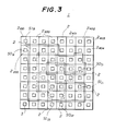
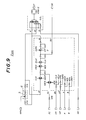
- FIG.3 shows an LSI chip I having input/output cells 2 arranged on the surface of the LSI chip 1.
- Each input/output cell 2 is provided with a pad 3.
- the input/output cells 2 for scan-in/out are arranged in the outer peripheral end region of the LSI chip 1, that is, in the peripheral part of the LSI chip 1.
- the pad 3 of the input cell 2 for scan-in is denoted by SI, while the pad 3 of the output cell for scan-out is denoted by SO.
- the input/output cells 2 for data input/output are arranged on the entire surface of the LSI chip 1.
- a boundary scan chain which is indicated by a bold line in FIG.3 or an internal (logic) scan chain which is indicated by a dotted line in FIG.3 is connected to each input/output cell 2 for scan-in/out as a scan path circuit.
- FIG.3 only shows a part of the input/output cells 2 for scan-in/out.
- the boundary scan which is one method of testing the LSI is originally intended to also confirm whether or not signal transfers are normally carried out between the LSIs.
- the boundary scan chain is used as a means of setting inputs to or reading outputs from those input/output cells 2 which cannot be contacted by the prober needles.
- the inputs to or the outputs from those input/output cells 2 which cannot be contacted by the prober needles are set or read out via the boundary scan chain.
- the boundary scan chain is a series loop which connects selected ones of a plurality of flip-flops (memory elements) existing in the input/output cells 2 which are arranged in the inner part of the LSI chip 1 by switching a mode signal to form a shift register, as shown in FIG.4.
- a test data having a logic value "1" or "0" is input from the scan-in pad 3 (SI B ) in synchronism with a scan clock signal, so as to successively write the test data into each flip-flop.
- SI B scan-in pad 3
- the input/output cells 2 for scan-in/out are arranged in the outermost peripheral part of the LSI chip 1, and the data is supplied to or is read from the input/output cells 2 located at the central part of the LSI chip 1 via the boundary scan chain.
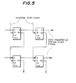
- the internal scan chain shown in FIG.5 is used.
- the data are successively written into the flip-flops which form the internal boundary chain via scan-in pads 3 (SI11, SI12) of the input/output cells 2 for scan-in which are arranged in the outermost peripheral part of the LSI chip 1 by the switching of the mode signal.
- the data are also written into the flip-flops existing within the input/output cells 2 of the LSI chip 1 via the boundary scan chain.
- the system clock signal is supplied again at the time when the write operations with respect to the internal scan chain and the boundary scan chain are completed.
- the test can be carried out by contacting the prober needles 14 to the pads 3 of the input/output cells 2 for scan-in/out which are arranged in the outermost peripheral part of the LSI chip 1, for either case where the boundary scan or the internal scan is made.
- the structure of the prober can be made simple as in the case of the conventional case.
- specific input/output cells 2 are made to function as the input/output cells for scan-in/out, however, arbitrary input/output cells 2 may be made to function as the input/output cells for scan-in/out.
- this embodiment uses independent input/output cells 2 for the input/output cell for use in the boundary scan and the input/output cell for use in the internal scan, it is possible to use the same input/output cell for either the boundary scan or the internal scan by switching the scan chain in response to the switching of the mode signal.
- FIG.7 shows an embodiment of the input/output cell which may be used as any one of the input/output cells 2100 and 2401 through 2404 shown in FIG.3.
- the input/output cell shown in FIG.7 is made up of inverters and transmission gates which are connected as shown, and the scan data is input thereto.
- FIG.8 shows an embodiment of the input/output cell which may be used as the input/output cell 2300 shown in FIG.3.
- the input/output cell shown in FIG.8 is made up of inverters and transmission gates which are connected as shown, and corresponds to a part of the scan circuit other than the input/output part thereof.
- FIG.9 shows another embodiment of the input/output cell which may be used as the input/output cell 2300 shown in FIG.3.
- the input/output cell shown in FIG.9 is made up of inverters and transmission gates which are connected as shown, and corresponds to a part of the scan circuit other than the input/output part thereof.
- the input/output cell shown in FIG.9 has an increased output driving capability compared to that of the input/output cell shown in FIG.8.
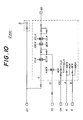
- FIG.10 shows an embodiment of the input/output cell which may be used as the input/output cell 2200 shown in FIG.3.
- the input/output cell shown in FIG.10 is made up of inverters and transmission gates which are connected as shown, and outputs the scan signal therefrom.
- a protection element (or circuit) 6 is connected to the pad 3.
- FIG.11 shows an embodiment of the scan circuit which is formed by the input/output cells having the constructions shown in FIGS.7, 8 and 10.
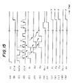
- Each of the input/output cells 2100, 2200 and 2300 output the data input to the scan-in terminal SI thereof from the scan-out terminal SO thereof with the timing shown in FIG.13 relative to scan clock signals A and B of the scan flip-flop used for making the scan operation.
- NFN denotes a control signal for controlling the tri-state
- IT denotes an input terminal
- OT denotes an output terminal
- CK denotes a clock signal of the scan flip-flop used for making the normal data read operation
- TCK denotes a clock signal applied to the flip-flops forming the internal scan chain
- UP denotes a clock signal for reading the content of the scan flip-flop into the latch circuit
- MD denotes a control signal for controlling the selector such as that shown in FIG.4.
- the control signals NFN and MD and the clock signal UP are generated from a test control circuit 9 which is provided in the LSI chip, while the clock signals A, B, CK and TCK are generated from a circuit shown in FIG.12.
- the boundary scan chain formed by the input/output cells 2100, 2200 and 2300 is coupled to the flip-flops forming the internal scan chain via a first internal logic circuit, and the flip-flops forming the internal scan chain is coupled to a second internal logic circuit.
- a part of the input/output cell 2200 surrounded by a dotted line in FIG.10 may be used as each flip-flop forming the internal scan chain.
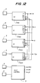
- FIG.12 shows an embodiment of the circuit which generates the various control signals and clock signals used in FIG.11.
- the circuit shown in FIG.12 includes the input/output cells 2401 through 2404 and the test control circuit 9.
- the input/output cells 2401 through 2404 respectively generate the clock signals CK, A, B and TCK.
- the clock signal CK is used to input the data held in the scan flip-flop to the scan flip-flop again via the pad 3, and to output the data to the first internal logic circuit.
- the scan clock signals A and B are used to shift the scan data pattern in the row of scan flip-flops within the input/output cells.
- the clock signal TCK is used to determine the timing with which the data from the first internal logic circuit is entered into the internal scan chain (internal scan circuit) which is indicated by the dotted line in FIG.3.
- the scan test can be carried out as follows. First, the clock signal UP is fixed to the low level and the clock signal CK is fixed to the high level, and the data pattern is entered into the scan flip-flops of the boundary scan chain and the internal scan chain in response to the clock signals A and B shown in FIG.13.
- the clock signal UP is set to the high level and the clock signal CK is set to the low level, and the data is transferred from each scan flip-flop of the boundary scan chain to the first internal logic circuit via the pad 3.
- the clock signal TCK is input to each scan flip-flop of the internal scan chain so as to output the data from each scan flip-flop of the internal scan chain to the second internal logic circuit and to input the data from the first internal logic circuit to the terminal D of each scan flip-flop of the internal scan chain.
- the data is output via each scan-out flip-flop in response to the clock signals A and B.
- FIG.14 shows a part of a second embodiment of the semiconductor integrated circuit according to the present invention.
- the circuit shown in FIG.14 corresponds to a test input circuit of the integrated circuit.
- external terminals 120 through 123 are the pads (or bumps) which are arranged in the peripheral part on the surface of the LSI (or semiconductor) chip such as that shown in FIG.3.
- a clear signal CL, a strobe signal STB, a data signal DATA for testing and a clock signal CLK are respectively input to the terminals 120, 121, 122 and 123.
- D-type flip-flops 1241 through 124 n are connected in series and forms a first shift register.
- the flip-flops 1241 through 124 n are cleared during a low-level period of the clear signal CL which is shown in FIG.15 (A) and is input from the terminal 120, and Q-terminals of the flip-flops 1241 through 124 n are set to the low level.
- the outputs from the Q-terminals of the flip-flops 1241 through 124 n are respectively supplied to latch circuits 1251 through 125 n .
- the latch circuits 1251 through 125 n have the same construction, and only the construction of the latch circuit 1251 is shown in FIG.14.
- Each latch circuit receives the clear signal CL from the terminal 120 and the strobe signal STB which is shown in FIG.15 (B) and is obtained from the terminal 121.
- the latch circuits 1251 through 125 n respectively make output signals X1 through X n thereof shown n FIG.15 (J) through (N) to the low level during the low-level period of the clear signal CL via respective NAND circuit 126 and inverter 127.
- the switch S1 is made up of a transmission gate 129 and an inverter 130 which inverts the strobe signal STB, as shown in FIG.16.
- the output from the Q-terminal of the corresponding one of the flip-flops 1241 through 124 n is supplied from a terminal 132 to the NAND circuit 126 during the high-level period of the strobe signal STB.
- the switch S2 is constructed similarly to the switch S1.
- the clear signal CL is input to a terminal 141
- the strobe signal STB is input to a terminal 142
- the output from the Q-terminal of the corresponding one of the flip-flops 1241 through 124 n is input to a terminal 143.
- the output signal X is output from a terminal 144.
- FIG.18 shows a modification of the semiconductor integrated circuit shown in FIG.14.
- those parts which are the same as those corresponding parts in FIG.14 are designated by the same reference numerals, and a description thereof will be omitted.
- an external terminal 150 corresponds to the pad which is arranged in the peripheral part on the surface of the LSI chip.
- a control signal CNTL shown in FIG.19 (A) is input to this external terminal 150 and is supplied to each of latch circuits 1511 through 151 n .
- the flip-flops 1241 through 12 n which form the shift register shift the data signal DATA shown in FIG.19 (B) in response to the clock signal CLK shown in FIG.19 (C), and the outputs from the Q-terminals of the flip-flops 1241 through 124 n shown in FIG.19 (D) through (F) are respectively supplied to the latch circuits 1511 through 151 n .
- each of the latch circuits 1511 through 151 n include inverters 156 and 157 for inverting the control signal CNTL from a terminal 155 to generate a control signal for transmission gates, a transmission gate 159 for supplying the output from the Q-terminal of the corresponding one of the flip-flops 1241 through 124 n received via a terminal 158 to inverters 160 and 161, and a transmission gate 162 for feeding back the output of the inverter 161 to the inverter 160 to form a latch loop.
- the transmission gate 59 closes and the signal Q from the terminal 158 is output from a terminal 163 as the output signal X.
- the transmission gate 162 closes and the output signal X is latched.
- the latch circuits 1511 through 151 n shown in FIG.18 respectively obtain the outputs from the Q-terminals of the flip-flops 1241 through 124 n during the high-level period of the control signal CNTL and output these outputs from the Q-terminals as the output signals X1 through X n to the pads at the central part on the surface of the LSI chip.
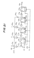
- FIG.21 shows another part of the second embodiment of the semiconductor integrated circuit according to the present invention.
- the circuit shown in FIG.21 corresponds to a test output circuit of the integrated circuit.
- external terminals 170 through 172 are the pads arranged at the peripheral part on the surface of the LSI chip.
- the control signal CNTL, the clock signal CK and the clear signal CL are respectively input to the terminals 170 through 172.
- Terminals 1741 through 1743 are the pads for output arranged at the central part on the surface of the LSI chip, and are respectively supplied with signal a , b and c which are output from an internal circuit.
- D-type flip-flops 1751 through 1754 are connected in series to form a second shift register, and are cleared during the low-level period of the clear signal CL shown in FIG.22 (A).
- NAND circuits 1761 through 1763 respectively invert the signals a , b and c shown in FIG.22 (B), (C) and (D) during the high-level period of the control signal CNTL shown in FIG.22 (E).
- the inverted signals from the NAND circuits 1761, 1762 and 1763 are respectively supplied to the flip-flops 1751, 1752 and 1753 via an inverter 1771 and NAND circuits 1772 and 1773, and the inverted signals are respectively set in the flip-flops 1751 through 1753 at the rising edge of the clock signal CK shown in FIG.22 (F).
- a high-level signal is set in the flip-flop 1754 via an inverter 1764 and a NAND circuit 1774 at the first rising edge of the clock signal CK.
- the test data which is serially input from the pad located at the peripheral part of the LSI chip is supplied to the pad located at the central part of the LSI chip via the flip-flops 1241 through 124 n which form the first shift register and the latch circuits 1251 through 125 n .
- the output signal from the pad located at the central part of the LSI chip is serially output from the pad located at the peripheral part of the LSI chip via the flip-flops 1751 through 1754 which form the second shift register. For this reason, it is possible to carry out the required test by making the probe needle contact the pad which is located at the peripheral part of the LSI chip.
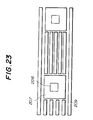
- the input/output cells are arranged at the inner part of the surface of the LSI chip. That is, as shown in FIG.23, the region of the LSI chip where logic circuits are to be formed becomes used up by an input/output cell 207, and in addition, the input/output cell 207 isolates basic cell rows 209. As a result, the integration density of the internal circuit of the LSI chip becomes poor.
- the input/output cell 207 is shown as having a pad 208.
- the input/output cell which is used to make the data transfer between semiconductor integrated circuits which are mounted on mutually differentsubstrates must use an output transistor which has a greater size compared to other transistors used within the semiconductor integrated circuits. For this reason, the input/output cell which is used for such a data transfer occupies a greater area than an input/output cell which is used for the data transfer within the same substrate. Accordingly, this difference in the sizes of the input/output cells depending on the usage thereof must be taken into consideration when arranging the input/output cells not only at the peripheral part but also at the inner part on the surface of the LSI chip.
- the input/output cells which occupy a small area compared to other input/output cells are mainly arranged at the inner part on the surface of the LSI chip, so as to minimize the deterioration of the integration density of the internal circuit of the LSI chip caused by the input/output cells which occupy a relatively large area compared to other input/output cells.
- the present invention is applied to the gate array type semiconductor integrated circuit.
- FIG.24 generally shows the concept of this embodiment.
- the LSI chip includes a chip body 212, an element forming surface 213, and input/output cells (or circuits) 214 and 215.
- the input/output cell 214 is used for the data transfer between a first substrate on which this embodiment is mounted and a second substrate which is different from the first substrate.
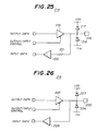
- FIG.25 shows the circuit construction of the input/output cell 214.
- the input/output cell 214 includes a pad 216, protection diodes 217 and 218, an output circuit 219, and input circuit 220, and an input protection resistor 221.
- the input/output cell 215 is used for the data transfer between LSI chips (semiconductor integrated circuits) which are mounted on the same first substrate.
- FIG.26 shows the circuit construction of the input/output cell 215.
- the input/output cell 215 includes a pad 222, protection diodes 223 and 224, an output circuit 225, and an input circuit 226.
- the area occupied by the protection diodes 217 and 218 of the input/output cell 214 is greater than the area occupied by the protection diodes 223 and 224 of the input/output cell 215, so that more strong measures are taken in the input/output cell 214 against electrostatic destruction.
- the size of the output transistor forming the output circuit 219 of the input/output cell 214 is greater than the size of the output transistor forming the output circuit 225 of the input/output cell 215, so that more strong measures are taken in the input/output cell 214 as regards the current driving capability of the output circuit 219.
- FIG.27 shows a cross section of the output transistor forming the output circuit 219 of the input/output cell 214.
- a silicon substrate 227 There are shown in FIG.27 a silicon substrate 227, a field oxide layer 228, a drain diffusion layer 229, a source diffusion layer 230, a gate oxide layer 231 and a gate 132.
- This output transistor has the drain diffusion layer 229 and the source diffusion layer 230 which are formed to a relatively deep part of the substrate 227 so as to increase the withstand voltage against electrostatic destruction.
- FIG.28 shows a cross section of the output transistor forming the output circuit 225 of the input/output cell 215.
- FIG.28 those parts which are the same as those corresponding parts in FIG.27 are designated by the same reference numerals, and a description thereof will be omitted.
- a drain diffusion layer 233 a source diffusion layer 234, silicide layers 235 and 236, a gate oxide layer 237 and a gate 238.
- This output transistor has the drain diffusion layer 233 and the source diffusion layer 234 which are formed to a relatively shallow part of the substrate 227.
- the silicide layers 235 and 236 are respectively formed on the drain diffusion layer 233 and the source diffusion layer 234 to reduce the resistances of the drain and source, so that a high-speed operation becomes possible.
- the input transistor forming the input circuit 220 of the input/output cell 214 has the drain diffusion layer and the source diffusion layer thereof which are formed to a relatively shallow part of the substrate, but no silicide layer is formed on the drain and source diffusion layers because the provision of the silicide layer would make the input transistor susceptible to electrostatic destruction.
- the input transistor forming the input circuit 226 of the input/output cell 215 is formed similarly to the output transistor shown in FIG.28.
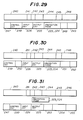
- FIGS.29 and 30 show cases where the input/output cells 215 are formed in the basic cell rows.
- FIG.31 shows a case where the protection diodes 223 and 224 of the input/output cell 215 are formed between the basic cell rows.
- a control circuit 239 is not shown in FIG.26, this control circuit 239 is used for the test.
- the logic circuits are formed in parts 240 through 255.
- a junction diode between the substrate and the drain diffusion layer of the output transistor which forms the output circuit 225 may be used in common as the protection diodes 223 and 224, and it is not essential to provide independent diodes exclusively as the protection diodes 223 and 224. The same can be said of the protection diodes 217 and 218 of the input/output cell 214.
- the input/output cells 214 which occupy a large area are arranged at the peripheral part on the surface 213 of the LSI chip, and the input/output cells 215 which occupy a relatively small area are arranged at the inner part of the surface 213 of the LSI chip. For this reason, the surface 213 of the LSI chip is effectively utilized, and the deterioration of the integration density of the internal circuit of the LSI chip is minimized.
- the present invention is applied to the gate array type semiconductor integrated circuit in this embodiment, the present invention can of course be applied to other types of semiconductor integrated circuits.
- the input/output cells in this embodiment are provided with the input circuit and the output circuit, the present invention can be applied similarly to the case where the input/output cells is only provided with the input circuit or the output circuit.
- FIG.32 which shows a cross section of a pad part of the conventional semiconductor integrated circuit, there are shown a field insulator layer 301, a lower conductor layer 311 which extends on the field insulator layer 301 and used as input/output interconnection, an insulator layer 312, an upper conductor layer 313, and a surface stablizing layer 314.
- pads 302 such as that shown in FIG.32 are arranged at the peripheral part of an LSI chip (semiconductor integrated circuit) 305 as shown in FIG.33.
- a testing circuit having the construction shown in FIG.34 was conventionally used to test the LSI chip 305.
- the testing circuit includes a boundary scan flip-flop 321, a selector 322, an output circuit 323, and an output circuit 324 which are connected as shown.
- the boundary scan flip-flop 321 includes a scan-in terminal SI which is connected to a scan-out terminal of a boundary scan flip-flop (not shown) which is provided on one side of the boundary scan flip-flop 321, a scan-out terminal SO which is connected to a scan-in terminal of another boundary scan flip-flop (not shown) which is provided on the other side of the boundary scan flip-flop 321, a data terminal D for entering data into this boundary scan flip-flop 321, a terminal CK for inputting a clock signal of a system circuit (not shown), and a clock terminal TCK for testing.
- the output circuit 323 outputs a signal L1 which is output from a logic circuit (not shown).
- the input circuit 32 inputs a signal L2 to the logic circuit.
- the pads 302 since it is desirable that a large number of pads 302 are provided on the LSI chip, it is desirable to arrange the pads 302 not only along one peripheral row of the LSI chip but along two or more rows or to distribute the pads 302 throughout the entire surface of the LSI chip.
- FIGS.35 and 36 A description will be given of a fourth embodiment of the semiconductor integrated circuit according to the present invention, by referring to FIGS.35 and 36.
- a pad of the LSI chip has the construction shown in FIG.35.
- lower conductor layers 331 and 332 which are respectively connected to mutually different logic circuits are formed on a field insulator layer 301.
- An upper conductor layer 334 is formed on the lower conductor layers 331 and 332 and an insulator layer 333, and short-circuits the lower conductor layers 331 and 332.
- a surface stabilizing layer 335 is formed on the surface as shown.
- a boundary scan flip-flop 321 includes a scan-in terminal SI which is connected to a scan-out terminal of a boundary scan flip-flop (not shown) which is adjacent to one side of the boundary scan flip-flop 321, a scan-out terminal SO which is connected to a scan-in terminal of a boundary scan flip-flop (not shown) which is adjacent to the other side of the boundary scan flip-flop 321, a data terminal D for entering data into the boundary scan flip-flop 321, a terminal CK for inputting a clock signal of a system circuit, and a clock terminal TCK for testing.
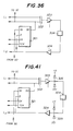
- a testing circuit shown in FIG.36 includes this boundary scan flip-flop 321, a selector 322, an output circuit 323, and an output circuit 324 which are connected as shown.
- the output circuit 323 outputs a signal L1 which is output from a logic circuit (not shown).
- the input circuit 32 inputs a signal L2 to the logic circuit.
- boundary scan chain is made via the pad 304, no boundary scan chain will be established if a conduction failure, short-circuit or the like exists within the pad 304 or in a region in the vicinity of the pad 304, it is possible to immediately find the conduction failure, short-circuit or the like.
- a data "1" is set in an arbitrary boundary scan flip-flop 321 via the boundary scan chain (terminal SI).
- the set data is output via the output circuit 323, the data is input to the boundary scan flip-flop 321 via the pad 304 and the input circuit 324 and the data is entered into the boundary scan flip-flop 321.
- a data which is next read into the boundary scan flip-flop 321 via the boundary scan chain (terminal SI) is read out by setting a data "0" into the boundary scan flip-flop 321.
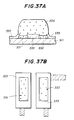
- FIGS.37A and 37B those parts which are the same as those corresponding parts in FIG.35 are designated by the same reference numerals, and a description thereof will be omitted.
- a bump 336 is provided in place of the upper conductor layer 334. Otherwise, this embodiment is the same as the fourth embodiment, and this embodiment functions similarly to the fourth embodiment.
- FIG.38 a description will be given of a sixth embodiment of the semiconductor integrated circuit according to the present invention, by referring to FIG.38.
- those parts which are the same as those corresponding parts in FIG.35 are designated by the same reference numerals, and a description thereof will be omitted.
- interconnections 337, 338, 339 and 340 are respectively connected to mutually different logic circuits. Hence, it is possible to selectively input external signals to a plurality of logic circuits and also selectively output signals from the plurality of logic circuits. Otherwise, this embodiment is the same as the fourth embodiment, and this embodiment functions similarly to the fourth embodiment.
- the probe needles do not need to contact all of the pads 304 due to the construction of each pad 304.
- the intervals of the pads 304 is freely selected as long as the bonding is possible, and the pads 304 are arbitrarily arranged on the LSI chip 305 as shown in FIG.39.
- FIG.40 a description will be given of an eighth embodiment of the semiconductor integrated circuit according to the present invention, by referring to FIG.40,
- those parts which are the same as those corresponding parts in FIG.39 are designated by the same reference numerals, and a description thereof will be omitted.
- the pads 304 are arranged in a matrix arrangement as shown in FIG.40.
- FIG.41 a description will be given of a ninth embodiment of the semiconductor integrated circuit according to the present invention, by referring to FIG.41.
- those parts which are the same as those corresponding parts in FIG.36 are designated by the same reference numerals, and a description thereof will be omitted.
- a protection circuit 325 is connected between the output circuit 323 and the pad 304, and between the input circuit 324 and the pad 304.
- Each protection circuit 325 is provided to protect the logic circuit and the like from external noise.
- the probe needles do not need to contact all of the pads 304 of this embodiment, and the pads 304 may be arranged as in the sixth and seventh embodiments described above.
Abstract
Description
- The present invention generally relates to semiconductor integrated circuits, and more particularly to a semiconductor integrated circuit having a scan path circuit which uses a scan-in/out system.
- The semiconductor technology has developed considerably over the recent years, and the integration density of semiconductor integrated circuits such as large scale integrated circuits (LSIs) and very large scale integrated circuits (VLSIs) has improved. Due to the increase in the integration density of the semiconductor integrated circuits, the number of terminals for data input/output has increased, and the number of input/output cells for data input/output has also increased. For this reason, it is impossible to secure the required number of input/output cells by the method of arranging the input/output cells only in a peripheral part of a chip of the semiconductor integrated circuit, and the input/output cells are now being arranged on the entire surface of the chip of the semiconductor integrated circuit. However, when the input/output cells are arranged on the entire surface of the chip, it is difficult to carry out a test which uses a prober.
- On the other hand, as the integration density of the semiconductor integrated circuit increases, it becomes more and more difficult to make a diagnosis on whether or not the semiconductor integrated circuit operates as originally designed. As a result, there is a problem in that the cost involved in testing the semiconductor integrated circuit increases. Accordingly, there are demands to realize a semiconductor integrated circuit which can facilitate the test and reduce the cost involved in testing the semiconductor integrated circuit.
- In the LSI production process, it is necessary to confirm the performance of the LSI. The test which is carried out to confirm the performance of the LSI can generally be divided into a test which is carried out at the development stage and a test which is carried out at the mass production stage. As the circuit test which is carried out at the mass production stage, there is a wafer probing test which is carried out at the end stage of the wafer process in order to reduce the defective chip mixture rate to the assembling process.
- According to the wafer probing test, tip ends of
needles 14 of the prober (not shown) make contact withcorresponding pads 15 of input/output cells 11 which are arranged on anLSI chip 10 as shown in FIG.1, and the electrical characteristics of theLSI chip 10 are checked by use of a signal generator, a waveform analyzer and the like which are coupled to the prober. As a result, it is possible to check not only the operation of theLSI chip 10 but also the transmission delay time, the rise time, the fall time and the like of signals. TheLSI chip 10 which is found to be defective as a result of this wafer probing test is automatically marked as a defective chip and is excluded from the subsequent assembling process. Hence, the chips which are found to be defective after the assembling process are only those which are generated in the assembling process, and it is possible to considerably improve the production yield and production cost of the LSI. - Conventionally, the integration density of the
LSI chip 10 is not extremely high and the number of input/output cells 11 is not extremely large. For this reason, the input/output cells 11 are provided at the outer peripheral end region of theLSI chip 10, that is, at the peripheral part of theLSI chip 10. Accordingly, it was sufficient to arrange theprober needles 14 which are required for the wafer probing test only at the peripheral part of theLSI chip 10. - But recently, due to the improved integration density of LSIs, it has become necessary to arrange the input/output cells for data input/output also at the inner part of the LSI chip. In order to carry out the wafer probing test similarly to the conventional case described above, it is necessary to arrange the
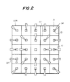
prober needles 14 which are required for the wafer probing test so as to make contact with thepads 15 of all of the input/output cells 11 within an LSI chip 10A, as shown in FIG.2. However, it is difficult to make a prober which has theprober needles 14 arranged to make contact with thepads 15 of all of the input/output cells 11 shown in FIG.2, and even if were possible to make such a prober, there are problems in that the prober would become expensive and the contact accuracy of theprober needles 14 would become poor. In addition, the testing equipment must be provided with a large number of terminals for supplying the signals to all of the input/output cells 11, and there is a problem in that the cost of the testing equipment itself becomes high. - Accordingly, it is a general object of the present invention to provide a novel and useful semiconductor integrated circuit in which the problems described above are eliminated.
- Another and more specific object of the present invention is to provide a semiconductor integrated circuit comprising a semiconductor chip body, a plurality of input/output cells arranged on a surface of the semiconductor chip body at parts including a peripheral part and a central part the semiconductor chip body, and at least an internal logic circuit provided on the semiconductor chip body, where each of the input/output cells include a pad and holding means coupled to the pad for holding incoming data, a plurality of the holding means are coupled in series in a test mode to form a scan path circuit, the input/output cell which has the pad for receiving an external test signal in a test mode is arranged at the peripheral part of the semiconductor chip body, and the test data held in the holding means of the input/output cell which is arranged at a part other than the peripheral part of the semiconductor chip body is transferred to the internal logic circuit in the test mode. According to the semiconductor integrated circuit of the present invention, it is possible to use a prober and a testing equipment which are similar to those conventionally used, Therefore, the prober needles can accurately contact the required pads and the testing can be carried out with ease using inexpensive prober and testing equipment which have simple constructions.
- Still another object of the present invention is to provide the semiconductor integrated circuit of the type described above wherein predetermined ones of the input/output cells having the pads for receiving an external signal and outputting a signal outside the semiconductor integrated circuit are arranged in the peripheral part of the semiconductor chip body, and the holding means which are coupled to form the scan path circuit include a first shift register for shifting the test data which is received from the input/output cell having the pad for receiving the external test signal in the test mode. According to the semiconductor integrated circuit of the present invention, it is possible to test the semiconductor integrated circuit by simply contacting the prober needles to those pads which are arranged in the peripheral part of the semiconductor integrated circuit.
- A further object of the present invention is to provide the semiconductor integrated circuit of the type described first, wherein predetermined ones of the input/output cells having the pads for receiving an external signal and outputting a signal outside the semiconductor integrated circuit are arranged in the peripheral part of the semiconductor chip body, first input/output cells are arranged in the peripheral part of the semiconductor chip body, second input/output cells are arranged in the central part of the semiconductor chip body, each first input/output cell is used for a data transfer between the semiconductor integrated circuit and another semiconductor integrated circuit which is independent from the semiconductor chip body, and each second input/output cell is primarily used for a data transfer within the semiconductor integrated circuit. According to the semiconductor integrated circuit of the present invention, it is possible to minimize the deterioration of the integration density of the internal logic circuit due to the provision of the input/output cells and effectively utilize the surface of the semiconductor chip body.
- Another object of the present invention is to provide the semiconductor integrated circuit of the type described first, wherein the semiconductor chip body includes a substrate, and the semiconductor integrated circuit further comprises a pair of lower conductor layers formed on the substrate and coupled to mutually different logic circuits within the semiconductor integrated circuit, and an upper conductor layer which is formed on the pair of lower conductor layers to short-circuit the pair of lower conductor layers, where the upper conductor layer forms the pad of the input/output cell. According to the semiconductor integrated circuit of the present invention, no boundary scan chain is established if a conduction failure, a short-circuit and the like occurs within the pad or in a vicinity of the pad. Hence, it is unnecessary to contact the prober needles to all of the pads in order to test the conduction test and the like within the pad or in the region in the vicinity of the pad. As a result, as long as the bonding is possible, there is no other limits to reducing the intervals of the pads, and the pads can be arranged using an arbitrary layout which efficiently utilizes the surface of the semiconductor chip body. Therefore, the integration density of the semiconductor integrated circuit can be improved.
- Still another object of the present invention is to provide a semiconductor integrated circuit comprising a semiconductor chip body, a plurality of input/output cells arranged on a surface of the semiconductor chip body, and at least an internal logic circuit provided on the semiconductor chip body, where the input/output cells include first input/output cells which are arranged in a peripheral part of the semiconductor chip body and second input/output cells which are arranged in a central part of the semiconductor chip body, each first input/output cell is used for a data transfer between the semiconductor integrated circuit and another semiconductor integrated circuit which is independent from the semiconductor chip body, and each second input/output cell is primarily used for a data transfer within the semiconductor integrated circuit. According to the semiconductor integrated circuit of the present invention, it is possible to minimize the deterioration of the integration density of the internal logic circuit due to the provision of the input/output cells and effectively utilize the surface of the semiconductor chip body.
- Other objects and further features of the present invention will be apparent from the following detailed description when read in conjunction with the accompanying drawings.
-
- FIG.1 is a diagram showing an LSI chip in a plan view for explaining an example of a conventional wafer probing test;
- FIG.2 is a diagram showing an LSI chip in a plan view for explaining another example of the conventional wafer probing test;
- FIG.3 is a plan view for explaining a first embodiment of a semiconductor integrated circuit according to the present invention;
- FIG.4 is a circuit diagram for explaining a scan chain;
- FIG.5 is a circuit diagram for explaining an internal scan chain;
- FIG.6 is a diagram showing the first embodiment in a plan view for explaining the testing thereof;
- FIGS.7 through 10 respectively are circuit diagrams showing embodiments of input/output cells shown in FIG.3;
- FIG.11 is a system block diagram showing an embodiment of a scan circuit which is formed by connecting the input/output cells having the constructions shown in FIGS.7, 8 and 10;
- FIG.12 is a system block diagram showing an embodiment of a circuit which generates various signals supplied to the scan circuit shown in FIG.11;
- FIG.13 is a timing chart for explaining the operation of the scan circuit shown in FIG.11;
- FIG.14 is a circuit diagram showing an essential part of a second embodiment of the semiconductor integrated circuit according to the present invention;
- FIG.15 is a timing chart for explaining the operation of the circuit shown in FIG.14;
- FIG.16 is a circuit diagram showing an embodiment of a switch shown in FIG.14;
- FIG.17 is a circuit diagram showing an embodiment of a latch circuit shown in FIG.14;
- FIG.18 is a circuit diagram showing a modification of the essential part of the second embodiment of the semiconductor integrated circuit according to the present invention;
- FIG.19 is a timing chart for explaining the operation of the circuit shown in FIG.18;
- FIG.20 is a circuit diagram showing an embodiment of a latch circuit shown in FIG.18;
- FIG.21 is a circuit diagram showing another essential part of the second embodiment of the semiconductor integrated circuit according to the present invention;
- FIG.22 is a timing chart for explaining the operation of the circuit shown in FIG.21;
- FIG.23 is a plan view for explaining considerations to be made when arranging the input/output cells on the LSI chip;
- FIG.24 is a plan view generally showing the concept of a third embodiment of the semiconductor integrated circuit according to the present invention;
- FIG.25 is a circuit diagram showing an embodiment of one input/output cell shown in FIG.24;
- FIG.26 is a circuit diagram showing an embodiment of another input/output cell shown in FIG.24;
- FIG.27 is a cross sectional view showing an output transistor which forms an output circuit of the input/output cell shown in FIG.25;
- FIG.28 is a cross sectional view showing an output transistor which forms an output circuit of the input/output cell shown in FIG.26;
- FIGS.29 and 30 respectively show cases where the input/output cells of the type shown in FIG.26 are formed in basic cell rows;
- FIG.31 shows a case where protection diodes of the input/output cell of the type shown in FIG.26 are formed between the basic cell rows;
- FIG.32 is a cross sectional view showing a pad part of the conventional semiconductor integrated circuit;
- FIG.33 is a plan view showing an arrangement of pads on the conventional semiconductor integrated circuit;
- FIG.34 is a circuit diagram showing a testing circuit conventionally used to test the conventional semiconductor integrated circuit;
- FIG.35 is a cross sectional view showing the construction of a pad of a fourth embodiment of the semiconductor integrated circuit according to the present invention;
- FIG.36 is a circuit diagram showing a testing circuit used to test the fourth embodiment of the semiconductor integrated circuit;
- FIGS.37A and 37B respectively are a cross sectional view and a plan view showing the construction of a pad of a fifth embodiment of the semiconductor integrated circuit according to the present invention;
- FIG.38 is a cross sectional view showing the construction of a pad of a sixth embodiment of the semiconductor integrated circuit according to the present invention;
- FIG.39 is a plan view showing an arrangement of pads of a seventh embodiment of the semiconductor integrated circuit according to the present invention;
- FIG.40 is a plan view showing an arrangement of pads of an eighth embodiment of the semiconductor integrated circuit according to the present invention; and
- FIG.41 is a circuit diagram showing an essential part of a ninth embodiment of the semiconductor integrated circuit according to the present invention.
- A description will be given of a first embodiment of a semiconductor integrated circuit according to the present invention, by referring to FIGS.3 through 6. In this embodiment, the present invention is applied to an LSI chip.
- FIG.3 shows an LSI chip I having input/
output cells 2 arranged on the surface of theLSI chip 1. Each input/output cell 2 is provided with apad 3. The input/output cells 2 for scan-in/out are arranged in the outer peripheral end region of theLSI chip 1, that is, in the peripheral part of theLSI chip 1. Thepad 3 of theinput cell 2 for scan-in is denoted by SI, while thepad 3 of the output cell for scan-out is denoted by SO. On the other hand, the input/output cells 2 for data input/output are arranged on the entire surface of theLSI chip 1. A boundary scan chain which is indicated by a bold line in FIG.3 or an internal (logic) scan chain which is indicated by a dotted line in FIG.3 is connected to each input/output cell 2 for scan-in/out as a scan path circuit. Of course, FIG.3 only shows a part of the input/output cells 2 for scan-in/out. - The boundary scan which is one method of testing the LSI is originally intended to also confirm whether or not signal transfers are normally carried out between the LSIs. But in this embodiment, the boundary scan chain is used as a means of setting inputs to or reading outputs from those input/
output cells 2 which cannot be contacted by the prober needles. In other words, the inputs to or the outputs from those input/output cells 2 which cannot be contacted by the prober needles are set or read out via the boundary scan chain. - The boundary scan chain is a series loop which connects selected ones of a plurality of flip-flops (memory elements) existing in the input/
output cells 2 which are arranged in the inner part of theLSI chip 1 by switching a mode signal to form a shift register, as shown in FIG.4. When making the test, a test data having a logic value "1" or "0" is input from the scan-in pad 3 (SIB) in synchronism with a scan clock signal, so as to successively write the test data into each flip-flop. By arbitrarily changing the content of the each flip-flop, it becomes possible to set each input/output cell 2 of theLSI chip 1 to an arbitrary state. On the other hand, when investigating the state of the input/output cell 2 of theLSI chip 1, a system clock signal is stopped so that the state of the input/output cell 2 will not change, and thereafter, the scan clock signal is input so as to output the state of the input/output cell 2 from the scan-out pad 3 (SOB). Therefore, the input/output cells 2 for scan-in/out are arranged in the outermost peripheral part of theLSI chip 1, and the data is supplied to or is read from the input/output cells 2 located at the central part of theLSI chip 1 via the boundary scan chain. - For example, when making a system failure diagnosis by checking the normal operation of an internal logic circuit provided in the
LSI chip 1, the internal scan chain shown in FIG.5 is used. In this case, the data are successively written into the flip-flops which form the internal boundary chain via scan-in pads 3 (SI₁₁, SI₁₂) of the input/output cells 2 for scan-in which are arranged in the outermost peripheral part of theLSI chip 1 by the switching of the mode signal. At the same time, the data are also written into the flip-flops existing within the input/output cells 2 of theLSI chip 1 via the boundary scan chain. The system clock signal is supplied again at the time when the write operations with respect to the internal scan chain and the boundary scan chain are completed. As a result, data transfers occur between the flip-flops existing within the internal scan chain and between the flip-flops existing within the boundary scan chain. Thereafter, the data of the flip-flops existing within the internal scan chain are read out via the scan-out pads 3 (SO₁₁, SO₁₂), and the data of the flip-flops existing within the boundary scan chain are read out via a scan-out pad 3 (SOB). In other words, the test is carried out by outputting the normal operation signal from the scan-out pads 3 (SO₁₁, SO₁₂) at specific timings while normally operating eachLSI chip 1. - Accordingly, as shown in FIG.6, the test can be carried out by contacting the prober needles 14 to the
pads 3 of the input/output cells 2 for scan-in/out which are arranged in the outermost peripheral part of theLSI chip 1, for either case where the boundary scan or the internal scan is made. For this reason, the structure of the prober can be made simple as in the case of the conventional case. In addition, because there is no need to increase the number of prober needles 14, it is possible to reduce the cost of the prober and the related testing equipment. - In this embodiment, specific input/
output cells 2 are made to function as the input/output cells for scan-in/out, however, arbitrary input/output cells 2 may be made to function as the input/output cells for scan-in/out. Furthermore, although this embodiment uses independent input/output cells 2 for the input/output cell for use in the boundary scan and the input/output cell for use in the internal scan, it is possible to use the same input/output cell for either the boundary scan or the internal scan by switching the scan chain in response to the switching of the mode signal. - FIG.7 shows an embodiment of the input/output cell which may be used as any one of the input/
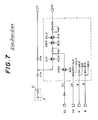
output cells - FIG.8 shows an embodiment of the input/output cell which may be used as the input/
output cell 2₃₀₀ shown in FIG.3. The input/output cell shown in FIG.8 is made up of inverters and transmission gates which are connected as shown, and corresponds to a part of the scan circuit other than the input/output part thereof. - FIG.9 shows another embodiment of the input/output cell which may be used as the input/
output cell 2₃₀₀ shown in FIG.3. The input/output cell shown in FIG.9 is made up of inverters and transmission gates which are connected as shown, and corresponds to a part of the scan circuit other than the input/output part thereof. The input/output cell shown in FIG.9 has an increased output driving capability compared to that of the input/output cell shown in FIG.8. - FIG.10 shows an embodiment of the input/output cell which may be used as the input/
output cell 2₂₀₀ shown in FIG.3. The input/output cell shown in FIG.10 is made up of inverters and transmission gates which are connected as shown, and outputs the scan signal therefrom. - In FIGS.7 through 9, a protection element (or circuit) 6 is connected to the
pad 3. - FIG.11 shows an embodiment of the scan circuit which is formed by the input/output cells having the constructions shown in FIGS.7, 8 and 10. Each of the input/
output cells - In FIG.11 and FIG.12 which will be described later, NFN denotes a control signal for controlling the tri-state, IT denotes an input terminal, OT denotes an output terminal, CK denotes a clock signal of the scan flip-flop used for making the normal data read operation, TCK denotes a clock signal applied to the flip-flops forming the internal scan chain, UP denotes a clock signal for reading the content of the scan flip-flop into the latch circuit, and MD denotes a control signal for controlling the selector such as that shown in FIG.4. The control signals NFN and MD and the clock signal UP are generated from a
test control circuit 9 which is provided in the LSI chip, while the clock signals A, B, CK and TCK are generated from a circuit shown in FIG.12. - In the case shown in FIG.11, the boundary scan chain formed by the input/
output cells output cell 2₂₀₀ surrounded by a dotted line in FIG.10 may be used as each flip-flop forming the internal scan chain. - FIG.12 shows an embodiment of the circuit which generates the various control signals and clock signals used in FIG.11. The circuit shown in FIG.12 includes the input/
output cells 2₄₀₁ through 2₄₀₄ and thetest control circuit 9. The input/output cells 2₄₀₁ through 2₄₀₄ respectively generate the clock signals CK, A, B and TCK. The clock signal CK is used to input the data held in the scan flip-flop to the scan flip-flop again via thepad 3, and to output the data to the first internal logic circuit. The scan clock signals A and B are used to shift the scan data pattern in the row of scan flip-flops within the input/output cells. The clock signal TCK is used to determine the timing with which the data from the first internal logic circuit is entered into the internal scan chain (internal scan circuit) which is indicated by the dotted line in FIG.3. - The scan test can be carried out as follows. First, the clock signal UP is fixed to the low level and the clock signal CK is fixed to the high level, and the data pattern is entered into the scan flip-flops of the boundary scan chain and the internal scan chain in response to the clock signals A and B shown in FIG.13.
- Second, the clock signal UP is set to the high level and the clock signal CK is set to the low level, and the data is transferred from each scan flip-flop of the boundary scan chain to the first internal logic circuit via the
pad 3. At the same time, the clock signal TCK is input to each scan flip-flop of the internal scan chain so as to output the data from each scan flip-flop of the internal scan chain to the second internal logic circuit and to input the data from the first internal logic circuit to the terminal D of each scan flip-flop of the internal scan chain. - Third, the data is output via each scan-out flip-flop in response to the clock signals A and B.
- FIG.14 shows a part of a second embodiment of the semiconductor integrated circuit according to the present invention. The circuit shown in FIG.14 corresponds to a test input circuit of the integrated circuit. In FIG.14,
external terminals 120 through 123 are the pads (or bumps) which are arranged in the peripheral part on the surface of the LSI (or semiconductor) chip such as that shown in FIG.3. A clear signal CL, a strobe signal STB, a data signal DATA for testing and a clock signal CLK are respectively input to theterminals - D-type flip-
flops 124₁ through 124n are connected in series and forms a first shift register. The flip-flops 124₁ through 124n are cleared during a low-level period of the clear signal CL which is shown in FIG.15 (A) and is input from the terminal 120, and Q-terminals of the flip-flops 124₁ through 124n are set to the low level. - Thereafter, the data signal DATA shown in FIG.15 (C) which is input from the terminal 122 is successively shifted in the flip-
flops 124₁ through 124n in response to the clock signal CLK which is shown in FIG.15 (D) and is input to the terminal 123. Hence, outputs from the Q-terminals of the flip-flops 124₁ through 124n are respectively set as shown in FIG.15 (E) through (I). - The outputs from the Q-terminals of the flip-
flops 124₁ through 124n are respectively supplied to latchcircuits 125₁ through 125n. Thelatch circuits 125₁ through 125n have the same construction, and only the construction of thelatch circuit 125₁ is shown in FIG.14. Each latch circuit receives the clear signal CL from the terminal 120 and the strobe signal STB which is shown in FIG.15 (B) and is obtained from the terminal 121. Thelatch circuits 125₁ through 125n respectively make output signals X₁ through Xn thereof shown n FIG.15 (J) through (N) to the low level during the low-level period of the clear signal CL viarespective NAND circuit 126 andinverter 127. In F1G.15 (J) through (N) and timing charts which follow, "H" denotes the high-level and "L" denotes the low level of the signal. When the level of the strobe signal STB becomes high, a switch S₁ closes, a switch S₂ opens in response to the strobe signal STB which is inverted by aninverter 128, and the output of theinverter 127 is fed back to theNAND circuit 126 so as to latch the corresponding one of the output signals X₁ through Xn. The output signals X₁ through Xn which are latched in thelatch circuits 125₁ through 125n are supplied to the pads located at the central part on the surface of the LSI chip. - The switch S₁ is made up of a
transmission gate 129 and aninverter 130 which inverts the strobe signal STB, as shown in FIG.16. The output from the Q-terminal of the corresponding one of the flip-flops 124₁ through 124n is supplied from a terminal 132 to theNAND circuit 126 during the high-level period of the strobe signal STB. The switch S₂ is constructed similarly to the switch S₁. - As shown in FIG.17, it is possible to use a latch circuit which is made up of
inverters 135 through 137 andNAND circuits 138 through 140 in place of each of thelatch circuits 125₁ through 125n shown in FIG.14. In this case, the clear signal CL is input to a terminal 141, the strobe signal STB is input to a terminal 142, and the output from the Q-terminal of the corresponding one of the flip-flops 124₁ through 124n is input to a terminal 143. The output signal X is output from a terminal 144. - FIG.18 shows a modification of the semiconductor integrated circuit shown in FIG.14. In FIG.18, those parts which are the same as those corresponding parts in FIG.14 are designated by the same reference numerals, and a description thereof will be omitted.
- In FIG.18, an
external terminal 150 corresponds to the pad which is arranged in the peripheral part on the surface of the LSI chip. A control signal CNTL shown in FIG.19 (A) is input to thisexternal terminal 150 and is supplied to each oflatch circuits 151₁ through 151n. The flip-flops 124₁ through 12n which form the shift register shift the data signal DATA shown in FIG.19 (B) in response to the clock signal CLK shown in FIG.19 (C), and the outputs from the Q-terminals of the flip-flops 124₁ through 124n shown in FIG.19 (D) through (F) are respectively supplied to thelatch circuits 151₁ through 151n. - As shown in FIG.20, each of the
latch circuits 151₁ through 151n includeinverters transmission gate 159 for supplying the output from the Q-terminal of the corresponding one of the flip-flops 124₁ through 124n received via a terminal 158 toinverters transmission gate 162 for feeding back the output of theinverter 161 to theinverter 160 to form a latch loop. During the high-level period of the control signal CNTL, the transmission gate 59 closes and the signal Q from the terminal 158 is output from a terminal 163 as the output signal X. In addition, during the low-level period of the control signal CNTL, thetransmission gate 162 closes and the output signal X is latched. - In other words, the
latch circuits 151₁ through 151n shown in FIG.18 respectively obtain the outputs from the Q-terminals of the flip-flops 124₁ through 124n during the high-level period of the control signal CNTL and output these outputs from the Q-terminals as the output signals X₁ through Xn to the pads at the central part on the surface of the LSI chip. - FIG.21 shows another part of the second embodiment of the semiconductor integrated circuit according to the present invention. The circuit shown in FIG.21 corresponds to a test output circuit of the integrated circuit. In FIG.21,
external terminals 170 through 172 are the pads arranged at the peripheral part on the surface of the LSI chip. The control signal CNTL, the clock signal CK and the clear signal CL are respectively input to theterminals 170 through 172. -
Terminals 174₁ through 174₃ are the pads for output arranged at the central part on the surface of the LSI chip, and are respectively supplied with signal a, b and c which are output from an internal circuit. - D-type flip-
flops 175₁ through 175₄ are connected in series to form a second shift register, and are cleared during the low-level period of the clear signal CL shown in FIG.22 (A).NAND circuits 176₁ through 176₃ respectively invert the signals a, b and c shown in FIG.22 (B), (C) and (D) during the high-level period of the control signal CNTL shown in FIG.22 (E). The inverted signals from theNAND circuits flops inverter 177₁ andNAND circuits flops 175₁ through 175₃ at the rising edge of the clock signal CK shown in FIG.22 (F). In addition, a high-level signal is set in the flip-flop 175₄ via aninverter 176₄ and aNAND circuit 177₄ at the first rising edge of the clock signal CK. - Thereafter, outputs from

flops 175₁ through 175₃ shown in FIG.22 (G) through (I) are respectively supplied to the flip-flops 175₂ through 175₄ of the next stage via theNAND circuits 177₂ through 177₄ every time the clock signal CK is received. As a result, the output from the Q-terminal of the flip-flop 175₄ shown in FIG.22 (J) is output via aterminal 178. This terminal 178 is the pad for output arranged at the peripheral part on the surface of the LSI chip. - Therefore, the test data which is serially input from the pad located at the peripheral part of the LSI chip is supplied to the pad located at the central part of the LSI chip via the flip-
flops 124₁ through 124n which form the first shift register and thelatch circuits 125₁ through 125n. In addition, the output signal from the pad located at the central part of the LSI chip is serially output from the pad located at the peripheral part of the LSI chip via the flip-flops 175₁ through 175₄ which form the second shift register. For this reason, it is possible to carry out the required test by making the probe needle contact the pad which is located at the peripheral part of the LSI chip. - For example, in a gate array type semiconductor integrated circuit, there basically are two problems if the input/output cells (or circuits) are arranged at the inner part of the surface of the LSI chip. That is, as shown in FIG.23, the region of the LSI chip where logic circuits are to be formed becomes used up by an input/
output cell 207, and in addition, the input/output cell 207 isolatesbasic cell rows 209. As a result, the integration density of the internal circuit of the LSI chip becomes poor. In FIG.23, the input/output cell 207 is shown as having apad 208. - Therefore, when arranging the input/output cells at not only the peripheral part on the surface of the LSI chip but also at the inner part on the surface of the LSI chip, it is necessary to use an arrangement which minimizes the deterioration of the integration density of the internal circuit of the LSI chip.
- On the other hand, in order to realize a high-speed operation of the semiconductor integrated circuit, there are demands to improve the data transfer speed between the semiconductor integrated circuits. In order to satisfy such demands, there are proposals to mount a plurality of semiconductor integrated circuits on a single substrate. However, the input/output cells are also required in this case to make the data transfer between the substrates.
- Generally, the input/output cell which is used to make the data transfer between semiconductor integrated circuits which are mounted on mutually differentsubstrates must use an output transistor which has a greater size compared to other transistors used within the semiconductor integrated circuits. For this reason, the input/output cell which is used for such a data transfer occupies a greater area than an input/output cell which is used for the data transfer within the same substrate. Accordingly, this difference in the sizes of the input/output cells depending on the usage thereof must be taken into consideration when arranging the input/output cells not only at the peripheral part but also at the inner part on the surface of the LSI chip.
- Next, a description will be given of a third embodiment of the semiconductor integrated circuit according to the present invention which takes the above into consideration, by referring to FIGS.24 through 32. In this embodiment, the input/output cells which occupy a small area compared to other input/output cells are mainly arranged at the inner part on the surface of the LSI chip, so as to minimize the deterioration of the integration density of the internal circuit of the LSI chip caused by the input/output cells which occupy a relatively large area compared to other input/output cells.
- In this embodiment, the present invention is applied to the gate array type semiconductor integrated circuit.
- FIG.24 generally shows the concept of this embodiment. In FIG.24, the LSI chip includes a
chip body 212, anelement forming surface 213, and input/output cells (or circuits) 214 and 215. The input/output cell 214 is used for the data transfer between a first substrate on which this embodiment is mounted and a second substrate which is different from the first substrate. - FIG.25 shows the circuit construction of the input/
output cell 214. The input/output cell 214 includes apad 216,protection diodes 217 and 218, anoutput circuit 219, andinput circuit 220, and aninput protection resistor 221. - On the other hand, the input/
output cell 215 is used for the data transfer between LSI chips (semiconductor integrated circuits) which are mounted on the same first substrate. - FIG.26 shows the circuit construction of the input/
output cell 215. The input/output cell 215 includes apad 222,protection diodes output circuit 225, and aninput circuit 226. - The area occupied by the
protection diodes 217 and 218 of the input/output cell 214 is greater than the area occupied by theprotection diodes output cell 215, so that more strong measures are taken in the input/output cell 214 against electrostatic destruction. - In addition, the size of the output transistor forming the
output circuit 219 of the input/output cell 214 is greater than the size of the output transistor forming theoutput circuit 225 of the input/output cell 215, so that more strong measures are taken in the input/output cell 214 as regards the current driving capability of theoutput circuit 219. - FIG.27 shows a cross section of the output transistor forming the
output circuit 219 of the input/output cell 214. There are shown in FIG.27 asilicon substrate 227, afield oxide layer 228, adrain diffusion layer 229, asource diffusion layer 230, agate oxide layer 231 and agate 132. This output transistor has thedrain diffusion layer 229 and thesource diffusion layer 230 which are formed to a relatively deep part of thesubstrate 227 so as to increase the withstand voltage against electrostatic destruction. - FIG.28 shows a cross section of the output transistor forming the
output circuit 225 of the input/output cell 215. In FIG.28, those parts which are the same as those corresponding parts in FIG.27 are designated by the same reference numerals, and a description thereof will be omitted. There are shown in FIG.28 a drain diffusion layer 233, asource diffusion layer 234, silicide layers 235 and 236, agate oxide layer 237 and agate 238. This output transistor has the drain diffusion layer 233 and thesource diffusion layer 234 which are formed to a relatively shallow part of thesubstrate 227. In addition, the silicide layers 235 and 236 are respectively formed on the drain diffusion layer 233 and thesource diffusion layer 234 to reduce the resistances of the drain and source, so that a high-speed operation becomes possible. - Although not shown, the input transistor forming the
input circuit 220 of the input/output cell 214 has the drain diffusion layer and the source diffusion layer thereof which are formed to a relatively shallow part of the substrate, but no silicide layer is formed on the drain and source diffusion layers because the provision of the silicide layer would make the input transistor susceptible to electrostatic destruction. In addition, the input transistor forming theinput circuit 226 of the input/output cell 215 is formed similarly to the output transistor shown in FIG.28. - FIGS.29 and 30 show cases where the input/
output cells 215 are formed in the basic cell rows. On the other hand, FIG.31 shows a case where theprotection diodes output cell 215 are formed between the basic cell rows. Although acontrol circuit 239 is not shown in FIG.26, thiscontrol circuit 239 is used for the test. Furthermore, in FIG.29 through 31, the logic circuits are formed inparts 240 through 255. - A junction diode between the substrate and the drain diffusion layer of the output transistor which forms the
output circuit 225 may be used in common as theprotection diodes protection diodes protection diodes 217 and 218 of the input/output cell 214. - According to this embodiment, the input/
output cells 214 which occupy a large area are arranged at the peripheral part on thesurface 213 of the LSI chip, and the input/output cells 215 which occupy a relatively small area are arranged at the inner part of thesurface 213 of the LSI chip. For this reason, thesurface 213 of the LSI chip is effectively utilized, and the deterioration of the integration density of the internal circuit of the LSI chip is minimized. - Although the present invention is applied to the gate array type semiconductor integrated circuit in this embodiment, the present invention can of course be applied to other types of semiconductor integrated circuits.
- In addition, although the input/output cells in this embodiment are provided with the input circuit and the output circuit, the present invention can be applied similarly to the case where the input/output cells is only provided with the input circuit or the output circuit.
- Next, a description will be given of the pad of the input/output cell of the conventional semiconductor integrated circuit, by referring to Figs.8 through 10.
- In FIG.32 which shows a cross section of a pad part of the conventional semiconductor integrated circuit, there are shown a
field insulator layer 301, alower conductor layer 311 which extends on thefield insulator layer 301 and used as input/output interconnection, aninsulator layer 312, anupper conductor layer 313, and asurface stablizing layer 314. - In the conventional semiconductor integrated circuit,
pads 302 such as that shown in FIG.32 are arranged at the peripheral part of an LSI chip (semiconductor integrated circuit) 305 as shown in FIG.33. - A testing circuit having the construction shown in FIG.34 was conventionally used to test the
LSI chip 305. In FIG.34, the testing circuit includes a boundary scan flip-flop 321, aselector 322, anoutput circuit 323, and anoutput circuit 324 which are connected as shown. The boundary scan flip-flop 321 includes a scan-in terminal SI which is connected to a scan-out terminal of a boundary scan flip-flop (not shown) which is provided on one side of the boundary scan flip-flop 321, a scan-out terminal SO which is connected to a scan-in terminal of another boundary scan flip-flop (not shown) which is provided on the other side of the boundary scan flip-flop 321, a data terminal D for entering data into this boundary scan flip-flop 321, a terminal CK for inputting a clock signal of a system circuit (not shown), and a clock terminal TCK for testing. Theoutput circuit 323 outputs a signal L₁ which is output from a logic circuit (not shown). The input circuit 32 inputs a signal L₂ to the logic circuit. - When testing the functions of the LSI chip using the above testing circuit, it is not essential to contact the probe needles (not shown) to all of the
pads 302 as long as the boundary scan chain is established. - However, in order to confirm the conducting state, the short-circuit and the like at a part A shown in FIG.34, it is necessary to contact the probe needles to all of the
pads 302 because the boundary scan chain is established even if a defect exists at this part A. - On the other hand, since it is desirable that a large number of
pads 302 are provided on the LSI chip, it is desirable to arrange thepads 302 not only along one peripheral row of the LSI chip but along two or more rows or to distribute thepads 302 throughout the entire surface of the LSI chip. - But as described above, in order to confirm the conducting state, the short-circuit and the like at the part A in FIG.34, it is necessary to contact the probe needles to all of the
pads 302, and for this reason, it is impossible to arrange thepads 302 in a large region of the LSI chip because the probe needles cannot be arranged to accurately contact all of thepads 302 in such a case. - Next, a description will be given of embodiments in which this problem can be eliminated.
- A description will be given of a fourth embodiment of the semiconductor integrated circuit according to the present invention, by referring to FIGS.35 and 36.
- In this embodiment, a pad of the LSI chip (semiconductor integrated circuit) has the construction shown in FIG.35. In FIG.35, lower conductor layers 331 and 332 which are respectively connected to mutually different logic circuits are formed on a
field insulator layer 301. Anupper conductor layer 334 is formed on the lower conductor layers 331 and 332 and aninsulator layer 333, and short-circuits the lower conductor layers 331 and 332. Asurface stabilizing layer 335 is formed on the surface as shown. - Next, a description will be given of the method of testing the LSI chip having a
pad 304 which has the construction shown in FIG.35, by referring to FIG.36. - In FIG.36, a boundary scan flip-
flop 321 includes a scan-in terminal SI which is connected to a scan-out terminal of a boundary scan flip-flop (not shown) which is adjacent to one side of the boundary scan flip-flop 321, a scan-out terminal SO which is connected to a scan-in terminal of a boundary scan flip-flop (not shown) which is adjacent to the other side of the boundary scan flip-flop 321, a data terminal D for entering data into the boundary scan flip-flop 321, a terminal CK for inputting a clock signal of a system circuit, and a clock terminal TCK for testing. A testing circuit shown in FIG.36 includes this boundary scan flip-flop 321, aselector 322, anoutput circuit 323, and anoutput circuit 324 which are connected as shown. Theoutput circuit 323 outputs a signal L₁ which is output from a logic circuit (not shown). The input circuit 32 inputs a signal L₂ to the logic circuit. - When testing the functions of the LSI chip using the above testing circuit, it is not essential to contact the probe needles (not shown) to all of the
pads 304 as long as the boundary scan chain is established. - In addition, because the boundary scan chain is made via the
pad 304, no boundary scan chain will be established if a conduction failure, short-circuit or the like exists within thepad 304 or in a region in the vicinity of thepad 304, it is possible to immediately find the conduction failure, short-circuit or the like. - Next, a more detailed description will be given of the testing operation.
- First, a data "1" is set in an arbitrary boundary scan flip-
flop 321 via the boundary scan chain (terminal SI). Second, when the set data is output via theoutput circuit 323, the data is input to the boundary scan flip-flop 321 via thepad 304 and theinput circuit 324 and the data is entered into the boundary scan flip-flop 321. Third, a data which is next read into the boundary scan flip-flop 321 via the boundary scan chain (terminal SI) is read out by setting a data "0" into the boundary scan flip-flop 321. - In this state, if a disconnection exists within the
pad 304 or in the region in the vicinity of thepad 304, the data which is set in the boundary scan flip-flop 321 via theinput circuit 324 is fixed to "1" or "0" and will not change, thereby enabling this defect to be found immediately. - According to this embodiment, it is unnecessary to contact the probe needles to all of the pads in order to test the conducting state within the pads or in the regions in the vicinities of the pads. For this reason, it is possible to distribute the pads on the LSI chip with an arbitrary arrangement.
- Next, a description will be given of a fifth embodiment of the semiconductor integrated circuit according to the present invention, by referring to FIGS.37A and 37B. In FIGS.37A and 37B, those parts which are the same as those corresponding parts in FIG.35 are designated by the same reference numerals, and a description thereof will be omitted.
- In this embodiment, a
bump 336 is provided in place of theupper conductor layer 334. Otherwise, this embodiment is the same as the fourth embodiment, and this embodiment functions similarly to the fourth embodiment. - Next, a description will be given of a sixth embodiment of the semiconductor integrated circuit according to the present invention, by referring to FIG.38. In FIG.38, those parts which are the same as those corresponding parts in FIG.35 are designated by the same reference numerals, and a description thereof will be omitted.
- In this embodiment,
interconnections - Next, a description will be given of a seventh embodiment of the semiconductor integrated circuit according to the present invention, by referring to FIG.39.
- In this embodiment, the probe needles do not need to contact all of the
pads 304 due to the construction of eachpad 304. Hence, the intervals of thepads 304 is freely selected as long as the bonding is possible, and thepads 304 are arbitrarily arranged on theLSI chip 305 as shown in FIG.39. - Next, a description will be given of an eighth embodiment of the semiconductor integrated circuit according to the present invention, by referring to FIG.40, In FIG.40, those parts which are the same as those corresponding parts in FIG.39 are designated by the same reference numerals, and a description thereof will be omitted.
- In this embodiment, the
pads 304 are arranged in a matrix arrangement as shown in FIG.40. - Next, a description will be given of a ninth embodiment of the semiconductor integrated circuit according to the present invention, by referring to FIG.41. In FIG.41, those parts which are the same as those corresponding parts in FIG.36 are designated by the same reference numerals, and a description thereof will be omitted.
- In this embodiment, a
protection circuit 325 is connected between theoutput circuit 323 and thepad 304, and between theinput circuit 324 and thepad 304. Eachprotection circuit 325 is provided to protect the logic circuit and the like from external noise. Of course, the probe needles do not need to contact all of thepads 304 of this embodiment, and thepads 304 may be arranged as in the sixth and seventh embodiments described above. - Further, the present invention is not limited to these embodiments, but various variations and modifications may be made without departing from the scope of the present invention.
Claims (32)
- A semiconductor integrated circuit characterized in that there are provided: a semiconductor chip body; a plurality of input/output cells (2, 214, 215) arranged on a surface of said semiconductor chip body at parts including a peripheral part and a central part said semiconductor chip body; and at least an internal logic circuit provided on said semiconductor chip body, each of said input/output cells (2, 214, 215) including a pad (3, 216, 222, 304) and holding means coupled to the pad for holding incoming data, a plurality of said holding means being coupled in series in a test mode to form a scan path circuit, the input/output cell (2) which has the pad (3) for receiving an external test signal in a test mode being arranged at the peripheral part of said semiconductor chip body, the test data held in the holding means of the input/output cell (2) which is arranged at a part other than the peripheral part of said semiconductor chip body being transferred to said internal logic circuit in the test mode.
- The semiconductor integrated circuit as claimed in claim 1, characterized in that predetermined ones of said input/output cells (2) having the pads (3) for receiving an external signal and outputting a signal outside the semiconductor integrated circuit are arranged in the peripheral part of said semiconductor chip body.
- The semiconductor integrated circuit as claimed in claim 2, characterized in that said predetermined input/output cells (2) are coupled to the scan path circuit.
- The semiconductor integrated circuit as claimed in claim 2 or 3, characterized in that the scan path circuit formed by the holding means is a boundary scan circuit.
- The semiconductor integrated circuit as claimed in claim 2 or 3, characterized in that the scan path circuit formed by the holding means is an internal scan circuit.
- The semiconductor integrated circuit as claimed in any of claims 2 to 5, characterized in that the holding means which are coupled to form the scan path circuit include a first shift register (124₁-124n) for shifting the test data which is received from the input/output cell (2) having the pad (3) for receiving the external test signal in the test mode.
- The semiconductor integrated circuit as claimed in claim 6, characterized in that the holding means which are coupled to form the scan path circuit further include latch circuits (125₁-125n) for latching output data received from corresponding stages of said first shift register (124₁-124n) and for supplying the data in parallel to the pads (3) of the input/output cells (2) which are arranged in the central part of said semiconductor chip body, and a second shift register (175₁-175₄) set with signals received from the pads (3) of the input/output cells (2) which are arranged in the central part of said semiconductor chip body at corresponding stages thereof and shifting the signals so as to serially output a signal from the pad (3) of an input/output cell (2) which is arranged in the peripheral part of said semiconductor chip body.
- The semiconductor integrated circuit as claimed in claim 6 or 7, characterized in that the pads (3) of said input/output cells (2) are arranged throughout the entire surface of said semiconductor chip body.
- The semiconductor integrated circuit as claimed in claim 2, characterized in that first input/output cells (214) are arranged in the peripheral part of said semiconductor chip body (212), second input/output cells (215) are arranged in the central part of said semiconductor chip body, each first input/output cell (214) is used for a data transfer between the semiconductor integrated circuit and another semiconductor integrated circuit which is independent from said semiconductor chip body, and each second input/output cell (215) is primarily used for a data transfer within the semiconductor integrated circuit.
- The semiconductor integrated circuit as claimed in claim 9, characterized in that the first and second input/output cells (214, 215) respectively include a protection diode (217, 218; 223, 224) which is coupled between the pad (216, 222) thereof and the internal logic circuit, and the protection diode (217, 218) of the first input/output cell (214) occupies an area on the surface of said semiconductor chip body greater than the area occupied by the protection diode (223, 224) of the second input/output cell (215).
- The semiconductor integrated circuit as claimed in claim 9 or 10, characterized in that the first and second input/output cells (214, 215) respectively include an output transistor, and the output transistor of the first input/output cell (214) has a size greater than that of the output transistor of the second input/output cell (215).
- The semiconductor integrated circuit as claimed in claim 11, characterized in that depths of drain and source diffusion layers (229, 230) of the output transistor of the first input/output cell (214) is greater than that of drain and source diffusion layers (233, 234) of the output transistor of the second input/output cell (215).
- The semiconductor integrated circuit as claimed in claim 12, characterized in that the drain and source diffusion layers (229, 230) of the output transistor of the first input/output cell (214) have a non-silicide surface, and the drain and source diffusion layers (233, 234) of the output transistor of the second input/output cell (215) have a silicide surface (235, 236).
- The semiconductor integrated circuit as claimed in any of claims 9 to 13, characterized in that the first input/output cell (214) includes an input transistor having a gate, and an input protection resistor (221) which is coupled in series between the gate of the input transistor and the pad (216) of the first input/output cell.
- The semiconductor integrated circuit as claimed in any of claims 9 to 14, characterized in that there are further provided rows of basic cells (209) arranged on the surface of said semiconductor chip body, and the second input/output cells (215) are arranged in the rows of the basic cells (209).
- The semiconductor integrated circuit as claimed in claim 15, characterized in that the second input/output cell (215) includes a protection diode (223, 224) which is coupled between the pad (222) thereof and the internal logic circuit, and each protection diode (223, 224) is formed between the rows of the basic cells (209).
- The semiconductor integrated circuit as claimed in claim 15, characterized in that the second input/output cell (215) includes a protection diode (223, 224) which is coupled between the pad (222) thereof and the internal logic circuit, and each protection diode (223, 224) is formed between the rows of the basic cells (209) and in the rows of the basic cells (209).
- The semiconductor integrated circuit as claimed in claim 1, characterized in that said semiconductor chip body includes a substrate (301), and the semiconductor integrated circuit further comprises a pair of lower conductor layers (331, 332) formed on the substrate (301) and coupled to mutually different logic circuits within the semiconductor integrated circuit, and an upper conductor layer (334) which is formed on the pair of lower conductor layers (331, 332) to short-circuit the pair of lower conductor layers, said upper conductor layer forming the pad (304) of the input/output cell.
- The semiconductor integrated circuit as claimed in claim 18, characterized in that the upper conductor layer (334) is formed as a bump.
- The semiconductor integrated circuit as claimed in claim 18 or 19, characterized in that there are further provided a plurality of input/output interconnections (339, 340) connected to the upper conductor layer (334).
- The semiconductor integrated circuit as claimed in any of claims 18 to 20, characterized in that the pads of the input/output cells are distributed with an arbitrary arrangement on the surface of said semiconductor chip body.
- The semiconductor integrated circuit as claimed in any of claims 18 to 20, characterized in that the pads of the input/output cells are arranged in a matrix arrangement on the surface of said semiconductor chip body.
- The semiconductor integrated circuit as claimed in any of claims 18 to 22, characterized in that each input/output cell includes an input circuit (324) coupled to the pad (304) thereof, an output circuit (323) coupled to the pad (304) thereof, and a pair of protection circuits (325) respectively coupled between the pad (304) and the input and output circuits (324, 323), said input circuit (324) and one of said protection circuits (325) are connected to one of said lower conductor layers (331, 332), and said output circuit (323) and the other of said protection circuits (325) are connected to the other of said lower conductor layers (331, 332).
- A semiconductor integrated circuit characterized in that there are provided: a semiconductor chip body (212); a plurality of input/output cells (214, 215) arranged on a surface (213) of said semiconductor chip body (212); and at least an internal logic circuit provided on said semiconductor chip body, said input/output cells (214, 215) including first input/output cells (214) which are arranged in a peripheral part of said semiconductor chip body (212) and second input/output cells (215) which are arranged in a central part of said semiconductor chip body (212), each first input/output cell being used for a data transfer between the semiconductor integrated circuit and another semiconductor integrated circuit which is independent from said semiconductor chip body, each second input/output cell being primarily used for a data transfer within the semiconductor integrated circuit.
- The semiconductor integrated circuit as claimed in claim 24, characterized in that the first and second input/output cells (214, 215) respectively include a protection diode (217, 218; 223, 224) which is coupled between the pad (216, 222) thereof and the internal logic circuit, and the protection diode (217, 218) of the first input/output cell (214) occupies an area on the surface (213) of said semiconductor chip body (212) greater than the area occupied by the protection diode (223, 224) of the second input/output cell (215).
- The semiconductor integrated circuit as claimed in claim 24 or 25, characterized in that the first and second input/output cells (214, 215) respectively include an output transistor, and the output transistor of the first input/output cell (214) has a size greater than that of the output transistor of the second input/output cell (215).
- The semiconductor integrated circuit as claimed in claim 26, characterized in that depths of drain and source diffusion layers (229, 230) of the output transistor of the first input/output cell (214) is greater than that of drain and source diffusion layers (233, 234) of the output transistor of the second input/output cell (215).
- The semiconductor integrated circuit as claimed in claim 27, characterized in that the drain and source diffusion layers (229, 230) of the output transistor of the first input/output cell (214) have a non-silicide surface, and the drain and source diffusion layers (233, 234) of the output transistor of the second input/output cell (215) have a silicide surface (235, 236).
- The semiconductor integrated circuit as claimed in any of claims 24 to 28, characterized in that the first input/output cell (214) includes an input transistor having a gate, and an input protection resistor (221) which is coupled in series between the gate of the input transistor and the pad (216) of the first input/output cell.
- The semiconductor integrated circuit as claimed in any of claims 24 to 29, characterized in that there are further provided rows of basic cells (209) arranged on the surface (213) of said semiconductor chip body (212), and the second input/output cells (215) are arranged in the rows of the basic cells (209).
- The semiconductor integrated circuit as claimed in claim 30, characterized in that the second input/output cell (215) includes a protection diode (223, 224) which is coupled between the pad (222) thereof and the internal logic circuit, and each protection diode (223, 224) is formed between the rows of the basic cells (209).
- The semiconductor integrated circuit as claimed in claim 30, characterized in that the second input/output cell (215) includes a protection diode (223, 224) which is coupled between the pad (222) thereof and the internal logic circuit, and each protection diode (223, 224) is formed between the rows of the basic cells (209) and in the rows of the basic cells (209).
Applications Claiming Priority (8)
| Application Number | Priority Date | Filing Date | Title |
|---|---|---|---|
| JP23841091A JP3287590B2 (en) | 1991-09-18 | 1991-09-18 | Semiconductor integrated circuit device |
| JP238410/91 | 1991-09-18 | ||
| JP3240010A JPH0580128A (en) | 1991-09-19 | 1991-09-19 | Semiconductor integrated circuit |
| JP240010/91 | 1991-09-19 | ||
| JP03241046A JP3111533B2 (en) | 1991-09-20 | 1991-09-20 | Semiconductor integrated circuit |
| JP241046/91 | 1991-09-20 | ||
| JP25495491A JP3170758B2 (en) | 1991-10-02 | 1991-10-02 | Semiconductor integrated circuit |
| JP254954/91 | 1991-10-02 |
Publications (3)
| Publication Number | Publication Date |
|---|---|
| EP0533476A2 true EP0533476A2 (en) | 1993-03-24 |
| EP0533476A3 EP0533476A3 (en) | 1994-03-23 |
| EP0533476B1 EP0533476B1 (en) | 1998-12-02 |
Family
ID=27477726
Family Applications (1)
| Application Number | Title | Priority Date | Filing Date |
|---|---|---|---|
| EP92308485A Expired - Lifetime EP0533476B1 (en) | 1991-09-18 | 1992-09-17 | Semiconductor integrated circuit with scan path |
Country Status (4)
| Country | Link |
|---|---|
| US (1) | US6487682B2 (en) |
| EP (1) | EP0533476B1 (en) |
| KR (1) | KR970001840B1 (en) |
| DE (1) | DE69227743T2 (en) |
Families Citing this family (7)
| Publication number | Priority date | Publication date | Assignee | Title |
|---|---|---|---|---|
| US6708238B1 (en) * | 2001-01-19 | 2004-03-16 | Sun Microsystems, Inc. | Input/output cell with a programmable delay element |
| JP2003121497A (en) * | 2001-10-09 | 2003-04-23 | Fujitsu Ltd | Scan path circuit for logic circuit test and integrated circuit device provided with it |
| US7281227B2 (en) * | 2004-09-30 | 2007-10-09 | Infineon Technologies Ag | Method and device for the computer-aided design of a supply network |
| JP5124904B2 (en) * | 2005-03-14 | 2013-01-23 | 日本電気株式会社 | Semiconductor test method and semiconductor device |
| KR100780775B1 (en) | 2006-11-24 | 2007-11-30 | 주식회사 하이닉스반도체 | Method for fabricating self assembled dummy pattern for semiconductor device by using circuitry layout |
| JP5625249B2 (en) * | 2009-03-24 | 2014-11-19 | 富士通株式会社 | Circuit module, semiconductor integrated circuit, and inspection apparatus |
| US8775108B2 (en) * | 2011-06-29 | 2014-07-08 | Duke University | Method and architecture for pre-bond probing of TSVs in 3D stacked integrated circuits |
Citations (8)
| Publication number | Priority date | Publication date | Assignee | Title |
|---|---|---|---|---|
| FR2508255A1 (en) * | 1981-06-22 | 1982-12-24 | Hitachi Ltd | INTEGRATED CIRCUIT DEVICE, REALIZED FROM A "STANDARD" MATRIX, REALIZING A MULTIPLICITY OF LOGIC FUNCTIONS BY MODIFICATION OF THE CALIBRATION NETWORK |
| JPS6034036A (en) * | 1983-08-04 | 1985-02-21 | Nec Corp | Master slice system lsi substrate |
| JPS60136241A (en) * | 1983-12-23 | 1985-07-19 | Toshiba Corp | Input circuit of gate array |
| JPS61179577A (en) * | 1985-02-04 | 1986-08-12 | Sumitomo Electric Ind Ltd | Semiconductor device and manufacture thereof |
| JPS62179742A (en) * | 1986-02-03 | 1987-08-06 | Seiko Epson Corp | Gate array |
| DE3715116A1 (en) * | 1986-05-07 | 1987-11-12 | Mitsubishi Electric Corp | INTEGRATED SEMICONDUCTOR CIRCUIT |
| JPH01259560A (en) * | 1988-04-08 | 1989-10-17 | Ricoh Co Ltd | Semiconductor integrated circuit device |
| JPH03203363A (en) * | 1989-12-29 | 1991-09-05 | Nec Corp | Semiconductor device |
Family Cites Families (36)
| Publication number | Priority date | Publication date | Assignee | Title |
|---|---|---|---|---|
| UST944007I4 (en) * | 1973-08-27 | 1976-03-02 | ||
| JPS57133644A (en) | 1981-02-12 | 1982-08-18 | Fujitsu Ltd | Semiconductor integrated circuit device |
| JPS6049648A (en) | 1983-08-30 | 1985-03-18 | Sumitomo Electric Ind Ltd | Master slice ic |
| US4819166A (en) * | 1983-08-31 | 1989-04-04 | Amdahl Corporation | Multimode scan apparatus |
| JPS6082871A (en) | 1983-10-13 | 1985-05-11 | Nec Corp | Logic integrated circuit |
| JPS60234341A (en) | 1984-05-07 | 1985-11-21 | Hitachi Ltd | Semiconductor integrated circuit device |
| JPS60242380A (en) | 1984-05-16 | 1985-12-02 | Hitachi Ltd | Facilitating circuit for fault diagnosis of integrated circuit |
| JPS60251643A (en) | 1984-05-28 | 1985-12-12 | Sharp Corp | Semiconductor gate array device |
| JPS6143464A (en) | 1984-08-08 | 1986-03-03 | Hitachi Ltd | Semiconductor device |
| JPS6154470A (en) | 1984-08-27 | 1986-03-18 | Toshiba Corp | Test facilitating circuit |
| JPS62126371A (en) | 1985-11-27 | 1987-06-08 | Nec Corp | Test signal generating circuit of digital circuit |
| JPS62154775A (en) | 1985-12-27 | 1987-07-09 | Hitachi Ltd | Logic integrated circuit |
| JPS62155549A (en) | 1985-12-27 | 1987-07-10 | Nec Corp | Large-scale integrated circuit |
| JPS62155550A (en) | 1985-12-27 | 1987-07-10 | Nec Corp | Large-scale integrated circuit |
| JPS62195169A (en) | 1986-02-21 | 1987-08-27 | Nec Corp | Large scale integrated circuit |
| JPS62224056A (en) | 1986-03-26 | 1987-10-02 | Hitachi Ltd | Semiconductor device |
| JPS63108747A (en) | 1986-10-27 | 1988-05-13 | Nec Corp | Gate array integrated circuit |
| JPS63243890A (en) | 1987-03-31 | 1988-10-11 | Toshiba Corp | Semiconductor integrated circuit device |
| JPS63300528A (en) | 1987-05-29 | 1988-12-07 | Nec Corp | Gate array integrated circuit |
| JPS6486536A (en) | 1987-09-29 | 1989-03-31 | Toshiba Corp | Semiconductor device |
| JPH01134280A (en) | 1987-11-19 | 1989-05-26 | Nec Corp | Gate array |
| JPH0758727B2 (en) | 1988-07-15 | 1995-06-21 | 沖電気工業株式会社 | Method for manufacturing semiconductor device |
| JPH02105468A (en) | 1988-10-13 | 1990-04-18 | Nec Corp | Field effect transistor circuit |
| JPH0330452A (en) | 1989-06-28 | 1991-02-08 | Hitachi Ltd | Semiconductor integrated circuit device |
| JPH0372281A (en) | 1989-08-14 | 1991-03-27 | Hitachi Ltd | Semiconductor integrated circuit device |
| JPH03165533A (en) | 1989-11-25 | 1991-07-17 | Seiko Epson Corp | Semiconductor device |
| DE4003453A1 (en) * | 1990-02-06 | 1991-08-08 | Bosch Gmbh Robert | CIRCUIT ARRANGEMENT FOR A ROTATING ANGLE POSITION DETECTION |
| JP2561164B2 (en) * | 1990-02-26 | 1996-12-04 | 三菱電機株式会社 | Semiconductor integrated circuit |
| JP2977959B2 (en) | 1991-07-12 | 1999-11-15 | シチズン時計株式会社 | Semiconductor device and measuring method thereof |
| US5347519A (en) * | 1991-12-03 | 1994-09-13 | Crosspoint Solutions Inc. | Preprogramming testing in a field programmable gate array |
| JP3227207B2 (en) | 1992-06-12 | 2001-11-12 | シチズン時計株式会社 | Semiconductor device and measuring method thereof |
| JPH06160489A (en) * | 1992-11-17 | 1994-06-07 | Hitachi Ltd | Boundary scan interior test system |
| DE69317221T2 (en) * | 1992-11-24 | 1998-10-01 | Advanced Micro Devices Inc | Scan test for integrated circuits |
| US5477545A (en) * | 1993-02-09 | 1995-12-19 | Lsi Logic Corporation | Method and apparatus for testing of core-cell based integrated circuits |
| JPH08101867A (en) * | 1994-09-30 | 1996-04-16 | Fujitsu Ltd | Software use permission system |
| US5487074A (en) * | 1995-03-20 | 1996-01-23 | Cray Research, Inc. | Boundary scan testing using clocked signal |
-
1992
- 1992-09-17 DE DE69227743T patent/DE69227743T2/en not_active Expired - Fee Related
- 1992-09-17 EP EP92308485A patent/EP0533476B1/en not_active Expired - Lifetime
- 1992-09-17 US US07/946,538 patent/US6487682B2/en not_active Expired - Fee Related
- 1992-09-18 KR KR1019920017009A patent/KR970001840B1/en not_active IP Right Cessation
Patent Citations (8)
| Publication number | Priority date | Publication date | Assignee | Title |
|---|---|---|---|---|
| FR2508255A1 (en) * | 1981-06-22 | 1982-12-24 | Hitachi Ltd | INTEGRATED CIRCUIT DEVICE, REALIZED FROM A "STANDARD" MATRIX, REALIZING A MULTIPLICITY OF LOGIC FUNCTIONS BY MODIFICATION OF THE CALIBRATION NETWORK |
| JPS6034036A (en) * | 1983-08-04 | 1985-02-21 | Nec Corp | Master slice system lsi substrate |
| JPS60136241A (en) * | 1983-12-23 | 1985-07-19 | Toshiba Corp | Input circuit of gate array |
| JPS61179577A (en) * | 1985-02-04 | 1986-08-12 | Sumitomo Electric Ind Ltd | Semiconductor device and manufacture thereof |
| JPS62179742A (en) * | 1986-02-03 | 1987-08-06 | Seiko Epson Corp | Gate array |
| DE3715116A1 (en) * | 1986-05-07 | 1987-11-12 | Mitsubishi Electric Corp | INTEGRATED SEMICONDUCTOR CIRCUIT |
| JPH01259560A (en) * | 1988-04-08 | 1989-10-17 | Ricoh Co Ltd | Semiconductor integrated circuit device |
| JPH03203363A (en) * | 1989-12-29 | 1991-09-05 | Nec Corp | Semiconductor device |
Non-Patent Citations (7)
| Title |
|---|
| IBM TECHNICAL DISCLOSURE BULLETIN. vol. 22, no. 7 , December 1979 , NEW YORK US pages 2772 - 2774 M.A. BATTISTA ET AL. 'Multiple function (I/O) cell layout' * |
| IBM TECHNICAL DISCLOSURE BULLETIN. vol. 27, no. 9 , February 1985 , NEW YORK US pages 534 - 5351 A. BRUSS ET AL. 'High Density CMOS standard image' * |
| PATENT ABSTRACTS OF JAPAN vol. 011, no. 004 (E-468)7 January 1987 & JP-A-61 179 577 (SUMITOMO ELECTRIC INDUSTRIES, LTD.) 12 August 1986 * |
| PATENT ABSTRACTS OF JAPAN vol. 014, no. 016 (E-872)12 January 1989 & JP-A-01 259 560 (RICOH CO LTD) 17 October 1989 * |
| PATENT ABSTRACTS OF JAPAN vol. 12, no. 24 (E-576)23 January 1988 & JP-A-62 179 742 (SEIKO EPSON CORPORATION) 6 August 1987 * |
| PATENT ABSTRACTS OF JAPAN vol. 9, no. 154 (E-325)(1877) 28 June 1985 & JP-A-60 034 036 (NIPPON DENKI K.K.) 21 February 1985 * |
| PATENT ABSTRACTS OF JAPAN vol. 9, no. 298 (E-361)(2021) 26 November 1985 & JP-A-60 136 241 (TOSHIBA K.K.) 19 July 1985 * |
Also Published As
| Publication number | Publication date |
|---|---|
| KR970001840B1 (en) | 1997-02-17 |
| US20020049927A1 (en) | 2002-04-25 |
| EP0533476A3 (en) | 1994-03-23 |
| US6487682B2 (en) | 2002-11-26 |
| EP0533476B1 (en) | 1998-12-02 |
| DE69227743T2 (en) | 1999-04-22 |
| DE69227743D1 (en) | 1999-01-14 |
Similar Documents
| Publication | Publication Date | Title |
|---|---|---|
| US5321277A (en) | Multi-chip module testing | |
| JP3103013B2 (en) | Multi-chip module with integrated test circuit and method of manufacturing the same | |
| US5115191A (en) | Testing integrated circuit capable of easily performing parametric test on high pin count semiconductor device | |
| US5509019A (en) | Semiconductor integrated circuit device having test control circuit in input/output area | |
| US5717700A (en) | Method for creating a high speed scan-interconnected set of flip-flop elements in an integrated circuit to enable faster scan-based testing | |
| US7348595B2 (en) | Semiconductor wiring substrate, semiconductor device, method for testing semiconductor device, and method for mounting semiconductor device | |
| US6094056A (en) | Multi-chip module with accessible test pads and test fixture | |
| US4812678A (en) | Easily testable semiconductor LSI device | |
| US4575674A (en) | Macrocell array having real time diagnostics | |
| KR910013711A (en) | Edge-Triggered Type D Flip-Flop Scan Latch Cell with Recycling Capability | |
| US6289477B1 (en) | Fast-scan-flop and integrated circuit device incorporating the same | |
| EP0414378B1 (en) | An adapter for integrated circuit elements and a method using the adapter for testing assembled elements | |
| US6487682B2 (en) | Semiconductor integrated circuit | |
| US6356095B1 (en) | Semiconductor integrated circuit | |
| EP0422912A2 (en) | Semiconductor integrated circuit device having test circuit | |
| US6640324B1 (en) | Boundary scan chain routing | |
| US6519728B2 (en) | Semiconductor integrated circuit having test circuit | |
| US6806731B2 (en) | Semiconductor integrated circuit device and fault-detecting method of a semiconductor integrated circuit device | |
| EP0213453A2 (en) | Noise reduction during testing of integrated circuit chips | |
| EP1224481B1 (en) | Apparatus and method for programmable parametric toggle testing of digital cmos pads | |
| KR0155590B1 (en) | Vlsi type impedence matching input terminator | |
| US7564255B2 (en) | Semiconductor integrated circuit for reducing number of contact pads to be probed in probe test | |
| US7032146B2 (en) | Boundary scan apparatus and interconnect test method | |
| US5958075A (en) | Efficient on-pitch scannable sense amplifier | |
| JP3287590B2 (en) | Semiconductor integrated circuit device |
Legal Events
| Date | Code | Title | Description |
|---|---|---|---|
| PUAI | Public reference made under article 153(3) epc to a published international application that has entered the european phase |
Free format text: ORIGINAL CODE: 0009012 |
|
| AK | Designated contracting states |
Kind code of ref document: A2 Designated state(s): DE FR GB |
|
| PUAL | Search report despatched |
Free format text: ORIGINAL CODE: 0009013 |
|
| AK | Designated contracting states |
Kind code of ref document: A3 Designated state(s): DE FR GB |
|
| 17P | Request for examination filed |
Effective date: 19940920 |
|
| 17Q | First examination report despatched |
Effective date: 19961202 |
|
| GRAG | Despatch of communication of intention to grant |
Free format text: ORIGINAL CODE: EPIDOS AGRA |
|
| GRAG | Despatch of communication of intention to grant |
Free format text: ORIGINAL CODE: EPIDOS AGRA |
|
| GRAH | Despatch of communication of intention to grant a patent |
Free format text: ORIGINAL CODE: EPIDOS IGRA |
|
| RBV | Designated contracting states (corrected) |
Designated state(s): DE |
|
| GRAH | Despatch of communication of intention to grant a patent |
Free format text: ORIGINAL CODE: EPIDOS IGRA |
|
| GRAA | (expected) grant |
Free format text: ORIGINAL CODE: 0009210 |
|
| AK | Designated contracting states |
Kind code of ref document: B1 Designated state(s): DE |
|
| REF | Corresponds to: |
Ref document number: 69227743 Country of ref document: DE Date of ref document: 19990114 |
|
| PLBE | No opposition filed within time limit |
Free format text: ORIGINAL CODE: 0009261 |
|
| STAA | Information on the status of an ep patent application or granted ep patent |
Free format text: STATUS: NO OPPOSITION FILED WITHIN TIME LIMIT |
|
| 26N | No opposition filed | ||
| PGFP | Annual fee paid to national office [announced via postgrant information from national office to epo] |
Ref country code: DE Payment date: 20070913 Year of fee payment: 16 |
|
| PG25 | Lapsed in a contracting state [announced via postgrant information from national office to epo] |
Ref country code: DE Free format text: LAPSE BECAUSE OF NON-PAYMENT OF DUE FEES Effective date: 20090401 |