EP0213453A2 - Noise reduction during testing of integrated circuit chips - Google Patents
Noise reduction during testing of integrated circuit chips Download PDFInfo
- Publication number
- EP0213453A2 EP0213453A2 EP86110981A EP86110981A EP0213453A2 EP 0213453 A2 EP0213453 A2 EP 0213453A2 EP 86110981 A EP86110981 A EP 86110981A EP 86110981 A EP86110981 A EP 86110981A EP 0213453 A2 EP0213453 A2 EP 0213453A2
- Authority
- EP
- European Patent Office
- Prior art keywords
- input
- chip
- driver
- tester
- output
- Prior art date
- Legal status (The legal status is an assumption and is not a legal conclusion. Google has not performed a legal analysis and makes no representation as to the accuracy of the status listed.)
- Granted
Links
Images

Classifications
-
- G—PHYSICS
- G01—MEASURING; TESTING
- G01R—MEASURING ELECTRIC VARIABLES; MEASURING MAGNETIC VARIABLES
- G01R31/00—Arrangements for testing electric properties; Arrangements for locating electric faults; Arrangements for electrical testing characterised by what is being tested not provided for elsewhere
- G01R31/28—Testing of electronic circuits, e.g. by signal tracer
- G01R31/316—Testing of analog circuits
-
- G—PHYSICS
- G01—MEASURING; TESTING
- G01R—MEASURING ELECTRIC VARIABLES; MEASURING MAGNETIC VARIABLES
- G01R31/00—Arrangements for testing electric properties; Arrangements for locating electric faults; Arrangements for electrical testing characterised by what is being tested not provided for elsewhere
- G01R31/28—Testing of electronic circuits, e.g. by signal tracer
- G01R31/317—Testing of digital circuits
- G01R31/3181—Functional testing
- G01R31/319—Tester hardware, i.e. output processing circuits
- G01R31/31917—Stimuli generation or application of test patterns to the device under test [DUT]
- G01R31/31924—Voltage or current aspects, e.g. driver, receiver
-
- G—PHYSICS
- G01—MEASURING; TESTING
- G01R—MEASURING ELECTRIC VARIABLES; MEASURING MAGNETIC VARIABLES
- G01R31/00—Arrangements for testing electric properties; Arrangements for locating electric faults; Arrangements for electrical testing characterised by what is being tested not provided for elsewhere
- G01R31/28—Testing of electronic circuits, e.g. by signal tracer
- G01R31/317—Testing of digital circuits
- G01R31/3181—Functional testing
- G01R31/319—Tester hardware, i.e. output processing circuits
- G01R31/3193—Tester hardware, i.e. output processing circuits with comparison between actual response and known fault free response
Definitions
- EP-A-132,522 published February 13, 1985, entitled “Oscillation Prevention During Testing of Integrated Circuit Logic Chips”.
- This invention relates to testing of integrated circuit logic chips and more particularly to excessive noise (Delta I) prevention during the testing thereof.
- delta I When many off chip drivers switch simultaneously a large change in power supply current results (delta I).
- This delta I current path flows from the driver output wire, through the driver, through the unbypassed inductance and resistance of the power supply distribution network, through the bypass capacitor and back to the tester ground.
- Voltage and current signals which change as a driver changes state also couple through mutual inductance and mutual capacitance into nearby I/O paths.
- Mutual inductance and mutual capacitance coupling may contribute, or solely result in false switching and test failures.
- the noise magnitude relates directly to the driver type (speed) and the number of drivers coupling noise into a nearby I/O path.
- the invention may be summarized as a driver sequencing network (DSN) on the integrated circuit device, or chip, to be tested which gives the tester (machine) control of the timing between the switching of groups of driver circuits so that more than a predetermined number of driver circuits concurrently switching state is precluded.
- the driver sequencing network is such that no one group of driver output pins can create enough delta I or coupled noise to cause a test failure.
- the driver sequencing network may be disabled to give full control of the driver outputs to the device being tested. In a normal application, i.e. the intended purpose or function of the device, the driver sequencing network is disabled.
- the function of the driver sequencing network is to control off chip driver switching during test. (An "off chip driver” is an output amplifier contained on the chip, to generate device output signals, also called off ship signals).
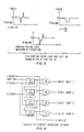
- FIG. 1 shows this delta I and its path from the driver output wire, through the driver, through the unbypassed inductance and resistance of the power supply distribution network, through the bypass capacitor and back to the tester ground.
- V MdI/dt
- I CdV/dt
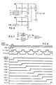
- FIG. 4 shows an example of a driver sequencing network. Inputs labeled “+ Inhibit,” “Shift In,” “L1 Clock,” and “L2 Clock” are controlled by the tester. Outputs “+ Inhibit Group 1" through “+ Inhibit Group 4" continue on the chip as the inhibit control lines for the respective off chip driver groups.
- the driver sequencing network shown is on the chip.
- DSN driver sequencing network
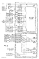
- FIG. 5 A preferred embodiment of the invention employing the driver sequence network can be seen in FIG. 5.
- the logic function internal to the chip is fed by a plurality of logical input receivers R5 through R54.
- the chip's logic function output is passed back to the tester through off chip drivers D2 through D1O2.
- Each driver D3 through D1O2 has at least one logic input and a driver inhibit input which, when active, blocks (inhibits) the logic state coming into the driver and forces the driver output to known or high impedance state.
- Driver D2 does not get inhibited in any circumstance.
- D2 is the commonly known shift register output of a Level Sensitive Scan Design (LSSD) register string.
- the LSSD register string is utilized in the chip logic function and enhances testability of that logic.
- FIG. 6 shows an example of a driver circuit with three logic inputs and an inhibit input
- FIG. 7 shows a corresponding logic diagram.
- All of the items listed above are fabricated on the chip and, except for the said driver inhibit inputs, are normal or conventional to a VLSI chip.
- a Driver Sequence Network To embody a Driver Sequence Network, additional receivers, drivers and logic is required.
- a representative DSN is shown enclosed within a broken line bearing the legend "Driver Sequencing Network" at the lower right of FIG. 6.
- the off chip drivers D3 through D1O2 are divided into ten groups of ten drivers each. Each group shares a common inhibit line so that there are ten separate group inhibit lines, one for each driver group. Again, D2 does not get inhibited because it provides the shift register output function.
- the group inhibit lines may all be set to the inhibiting state simultaneously by the "+ Inhibit" control line or each group inhibit line may be brought up sequentially by using the "Sequence Scan In', "+L1 Clock', and “+L2 Clock' to shift a logical "1' through the ten shift register latches (L1 through L1O).
- the "+ Inhibit” line may allow all group inhibit lines to go to the enable state simultaneously, or each line may be enabled sequentially by shifting a logical "O' through the ten latches (See FIG. 8 for a timing diagram of the shift operation; the shifting of a logical "1' is shown).
- Driver D1 facilitates testing of the sequencing shift register of the DSN by providing a shift register output to the tester.
- test execution steps can be used to prevent too many off chip drivers from switching simultaneously.
Abstract
Description
- EP-A-132,522 published February 13, 1985, entitled "Oscillation Prevention During Testing of Integrated Circuit Logic Chips".
- This invention relates to testing of integrated circuit logic chips and more particularly to excessive noise (Delta I) prevention during the testing thereof.
- During application of functional test patterns on VLSI (very large scale integration) devices electrical noise is generated on either the power supply or I/O (input/output) lines such that the internal logic state of the device becomes unpredictable and the test measurement fails. Electrical noise of significant magnitude is generated in two fashions by the switching of off chip drivers as more fully described below.
- When many off chip drivers switch simultaneously a large change in power supply current results (delta I). This delta I current path flows from the driver output wire, through the driver, through the unbypassed inductance and resistance of the power supply distribution network, through the bypass capacitor and back to the tester ground. The voltage that is generated across the unbypassed inductance and resistance is expressed as follows, V = LdI/dt + RdI, where V is the generated voltage, L is the unbypassed inductance, R is resistance, dI is delta I and dI/dt is the rate of change of the current I with respect to time. DI and dI/dt relate directly to the driver type and the number of drivers concurrently switching, as does the noise magnitude.
- Voltage and current signals which change as a driver changes state also couple through mutual inductance and mutual capacitance into nearby I/O paths. Mutual inductance and mutual capacitance coupling may contribute, or solely result in false switching and test failures. The voltage and current due to coupling is expressed by the equations V = MdI/dt and I = CdV/dt, where M is the mutual inductance, C is the mutual capacitance between the paths, and dV/dt is the rate of change of voltage with respect to time. Again the noise magnitude relates directly to the driver type (speed) and the number of drivers coupling noise into a nearby I/O path.
- Alternative solutions for this problem can be attempted:
- A) Modify the tester. This has been done. However sophisticated electrical noise still appears. The product design cycle is fast outstripping the testers ability to compensate.
- B) Pre-Charge Output Lines. This technique allows as many drivers to switch as the pattern dictates, but does not allow them to switch until the tester precharges all of the output lines to their expected state before switching occurs. Once switched, each output termination by the tester must be returned to its proper value before the outputs can be measured. This method is useful, but has three main drawbacks:
- 1) Test time increases considerably; 2) The performance and real estate overhead is high for the chip designer; 3) The expected output states must be known at the time of execution of each test pattern. This is inconsistent with the self test philosophy which logs output states for each pattern and compares them to expected states long after pattern execution is complete.
- C) Test pattern control of the number of outputs switching. This assumes the part number (i.e., the device to be tested) will allow itself to be limited to a specific number of drivers switching and still be able to achieve greater than 99.5% test coverage. The greater problem however, is that the simulator must apply patterns in the exact fashion the tester employs them. Most test machines apply all input changes serially which would cause excessive simulation time for software control of driver switching.
- D) The employment of an on-chip (or device contained) Driver Sequencing Network of improved design in accordance with applicants invention as fully disclosed hereinafter.
- Reference is made to U.S. Patent No. 4,441,O75 entitled "Electric Chip-In-Place Test (ECIPT) Structure and Method" granted April 3, 1984 to P. Goel et al, and to "Driver Sequencing Circuit" by D.C. Banker, F. A. Montegari and J.P. Norsworthy, IBM Technical Disclosure Bulletin, Vol. 26, No. 7B, December 1983, pages 3621-2.
- A number of test techniques, testers and test circuitry for testing integrated circuit devices are known to the art. It is to be appreciated with reference to the subject invention, that the following art is not submitted to be the only prior art, the best prior art, or the most pertinent prior art.
- 3,599,161 entitled "Computer Controlled Test System And Method" granted August 1O, 1971 to A.M. Stoughton et al.
3,694,632 entitled "Automatic Test Equipment Utilizing a Matrix of Digital Differential Analyzer Integrators To Generate Interrogation Signals" granted September 26, 1972 to D.J. Bloomer.
3,784,91O entitle "Sequential Addressing Network Testing System" granted January 8, 1974 to T.P. Sylvan.
3,848,188 entitled "Multilayer Control System For A Multi-Array Test Probe Assembly" granted November 12, 1974 to F.J. Ardezzone et al.
3,873,818 entitled "Electronic Tester For Testing Devices Having A High Circuit Density" granted March 25, 1975 to J.D. Barnard.
3,924,144 entitled "Method For Testing Logic Chips and Logic Chips Adapted Therefor" granted December 2, 1975 to G. Hadamard.
3,961,251 entitled "Testing Embedded Arrays" granted June 1, 1976 to W.J. Hurley et al.
3,976,94O entitled "Testing Circuit" granted August 24, 1976 to Y.B. Chau.
4,O66,882 entitled "Digital Stimulus Generating And Response Measuring Means" granted January 3, 1978 to C.M. Esposito.
4,O7O,565 entitled "Programmable Tester Method And Apparatus" granted January 24, 1978 to R.N. Borrell.
4,125,763 entitled "Automatic Tester For Microprocessor Board" granted November 14, 1978 to R.B. Drabing et al.
4,18O,2O3 entitled "Programmable Test Point Selector Circuit" granted December 25, 1979 to H.M. Masters.
4,216,539 entitled "In-Circuit Digital Tester" granted August 5, 198O to D.W. Raymond et al.
4,298,98O entitled "LSI Circuitry Comforming to Level Sensitive Scan Design (LSSD) Rules and Method of Testing Same" granted November 3, 1981 to J. Hajder et al.
4,334,31O entitled "Noise Suppressing BiLevel Data Signal Driver Circuit Arrangement" granted June 8, 1982 to G.A. Maley.
4,348,759 entitled "Automatic Testing Of Complex Semiconductor Components With Test Equipment Having Less Channels Than Those Required by The Component Under Test" granted September 7, 1982 to H.D. Schnurmann.
4,398,1O6 entitled "On-Chip Delta-I Noise Clamping Circuit" granted August 9, 1983 to E.E. Davidson et al.
4,441,O75 entitled "Electrical Chip-In-Place Test (ECIPT) Structure And Method" granted April 3, 1984 to P. Goel et al.
4,494,O66 entitled "Method of Electrically Testing a Packaging Structure Having N Interconnected Integrated Circuit Chips" granted January 15, 1985 to P. Goel et al.
4,5O4,784 entitled "Method Of Electrically Testing A Packaging Structure Having N Interconnected Integrated Circuit Chips" granted March 12, 1985 to P. Goel et al. - "Logic Structure For Testing Tri-State Drivers" by S. DasGupta and C.E. Radke, Vol. 21, No. 7, December 1978, pages 2796-7.
"Driver Power Distribution" by A.E. Barish and R.L. Ehrlickman, Vol. 22, No. 11, April 198O, pages 4935-7.
"Functionally Independent A.C. Test For Multi-Chip Package" by P. Goel and M.T. McMahon, Vol. 25, No. 5, October 1982, pages 23O8-1O.
"Chip Partitioning Aid" by M.C. Graf and R.A. Rasmussen, Vol. 25, No. 5, October 1982, pages 2314-5.
"Driver Sequencing Circuit" by D.C. Banker, F.A. Montegari and J.P. Norsworthy, Vol. 26, No. 7B, December 1983, pages 3621-2. - The invention may be summarized as a driver sequencing network (DSN) on the integrated circuit device, or chip, to be tested which gives the tester (machine) control of the timing between the switching of groups of driver circuits so that more than a predetermined number of driver circuits concurrently switching state is precluded. The driver sequencing network is such that no one group of driver output pins can create enough delta I or coupled noise to cause a test failure. The driver sequencing network may be disabled to give full control of the driver outputs to the device being tested. In a normal application, i.e. the intended purpose or function of the device, the driver sequencing network is disabled. The function of the driver sequencing network is to control off chip driver switching during test. (An "off chip driver" is an output amplifier contained on the chip, to generate device output signals, also called off ship signals).
- Accordingly, the objects of the invention are:
- 1) to improve the efficiency and reliability of the testing of integrated circuit devices and/or chips;
- 2) to provide a drive sequencing network (DSN) on an integrated circuit device, or chip, which permits a test machine to control the switching time of driver circuits (or groups of driver circuits) of the integrated circuit device, or chip, under test;
- 3) to improve the flexibility, efficiency and reliability of the testing of integrated circuit logic chips by applying tester control for significantly if not totally obviating the "delta I" problem due to simultaneous switching of drivers during test;
- 4) to provide a driver sequencing network on a logic chip, or the like, to sequence, under tester control, the switching of drivers, or groups of drivers, during test.
- These and other features and advantages of the invention will be apparent from the following more particular description of the preferred embodiment of the invention as illustrated in the accompanying drawings.
-
- FIG. 1 illustrates, in accordance with the prior art, the delta I current path from the driver output wire, through the driver, through the unbypassed inductance and resistance of the power supply distribution network, through the bypass capacitor and back to the tester ground; the incorporation of a DSN according to the invention is also illustrated.
- FIG. 2 is comprised of FIGS. 2A, 2B and 2C.
- FIG. 2A depicts a voltage waveform imposed on the driver output wire by an off chip driver during switching.
- FIG. 2B depicts a delta I waveform which occurs on the delta I path shown in the circuitry of FIG. 1.
- FIG. 2C depicts the voltage generated across the unbypassed inductance and resistance of the prior art circuitry of FIG. 1.
- FIG. 3 is comprised of FIGS. 3A, 3B and 3C.
- FIG. 3A depicts the coupled voltage V = MdI/dt of the prior art circuitry of FIG. 1.
- FIG. 3B depicts the coupled current I = CdV/dt of the prior art circuit of FIG. 1.
- FIG. 3C depicts the combined voltage noise waveform at the output of the prior art circuitry of FIG. 1.
- FIG. 4 shows a representative driver sequencing network in accordance with the invention.
- FIG. 5 shows a preferred embodiment of the invention wherein an integrated circuit chip under test includes a driver sequence network (DSN).
- FIG. 6 illustrates a representative driver circuit, having three logic inputs, an inhibit input and an output.
- FIG. 7 shows a block diagram of the driver circuit of FIG. 6.
- FIG. 8 shows a timing diagram to be reviewed in conjunction with the explanation of operation of the invention as illustrated in FIG. 5.
- When many off chip drivers switch simultaneously a large change in power supply current results (delta I). FIG. 1 shows this delta I and its path from the driver output wire, through the driver, through the unbypassed inductance and resistance of the power supply distribution network, through the bypass capacitor and back to the tester ground. FIG. 2C shows the voltage that is generated across the unbypassed inductance and resistance as expressed by V = LdI/dt + RdI. DI and dI/dt relate directly to the driver type and the number of drivers switching together, as does the noise.
- Voltage and current signals which change as a driver changes state can also couple into nearby I/O paths to such an extent that false switching and test failures occur. FIG. 3 shows the voltage and current that can be coupled as expressed by the equations V = MdI/dt and I = CdV/dt, where M is the mutual inductance and C is the mutual capacitance between the paths. Again the noise relates directly to the driver type (speed) and the number of drivers coupling noise into a nearby I/O path.
- FIG. 4 shows an example of a driver sequencing network. Inputs labeled "+ Inhibit," "Shift In," "L1 Clock," and "L2 Clock" are controlled by the tester. Outputs "+ Inhibit
Group 1" through "+ InhibitGroup 4" continue on the chip as the inhibit control lines for the respective off chip driver groups. The driver sequencing network shown is on the chip. - The four latches in FIG. 4 labeled "L1 Latch" and "L2 Latch" are chained together into the commonly known shift register configuration. Data applied at the "Shift In" input will be sequentially passed to successive latches as the L1 clock and L2 clock are alternately applied. The OR blocks shown allow either the "+ Inhibit" input or the shift register contents to control the four "+ Inhibit Group" outputs. The "+ Shift Out" output is available to the tester for testing of the shift register string.
- In the operation then: 1) Let "+ Inhibit" = "logical 1 state" thereby inhibiting all off chip drivers by setting a "logical 1" on all "+Inhibit Group" lines. 2) Now the shift register can be preset to a known state (all latch outputs = "logical 1" without worrying about off chip driver switching. 3) Next, change "+ Inhibit" = "logical O". The off chip drivers are sill inhibited by the latch contents. 4) Finally let "Shift In" = "logical O" and sequentially shift the "logical O" (by alternating L1 and L2 Clocks) until all latch outputs are a "logical O". In doing this we have sequentially enabled the groups of drivers with a separation between the groups equal to the separation between the L1 clock and the L2 clock. 5) To sequentially disable the off chip drivers, set "Shift In" = "logical 1" and then sequentially shift the "logical 1" onto all four latch outputs. 6) In normal system operation both "+ Inhibit" and "Shift In" must be a logical O. The L1 Clock and L2 Clock must both be kept at their active logic level so that the Shift In data ("logical O") will be kept on the latch outputs. The off chip drivers will always be enabled in this case.
- It should be noted that adding latches to the shift string, and corresponding "OR' gates, allows control over a greater number of off chip driver groups. For example:
Assume 24O off chip drivers on the chip.
Assume 12 groups are formed (by design). Therefore 2O drivers per group are allowed and 6L1 Latches 6 L2 latches and 12 OR gates are required to control the 12 groups. - No additional connections are required to the tester.
- A latent ability exists which would allow selective enabling of off chip drivers by presetting the shift register while the drivers are inhibited, then changing "+ Inhibit" to "O" to allow the preset shift register to enable the driver groups selected.
- The advantages and disadvantages of the driver sequencing network (DSN) are:
- 1) Flexible - The DSN can be employed or ignored as desired. Problem part numbers may require the DSN to be used whenever a test pattern called for the drivers to be enabled. The drivers will be sequence enabled, measured, and then sequence inhibited for each such pattern.
- 2) Driver Groups - Each group may be designed to minimize both coupled and power supply noise through physical selection of the driver placement for each group. In addition, troublesome drivers can be restricted to a specific number per group, instead of just by the group size.
- 3) Easily Implemented - Requires no new test hardware and relatively small changes to test generation.
- 4) Tester controlled sequencing - The tester has full control of the time separation between groups of switching drivers.
- 5) Low overhead - Low circuit count in DSN and no performance penalty for the user of the device.
- 6) Compatible - The DSN is compatible with electronic chip in place testing (ECIPT) partitioning (ECIPT is fully disclosed in the above-cited U.S. Patent No. 4,5O4,784 entitled "Method of Electronically Testing A Packaging Structure Having Integrated Circuit Chips"), driver inhibit pin techniques, and self test concepts.
- 7) Shipped Product Quality Level (SPQL) - Since the DSN is uniquely a testing aid, it need not be tested for full fault coverage. The small circuit count and minimal interface to the device logic makes the DSN a negligible contributor to device yield loss and SPQL.
- 8) The DSN is not readily useable at the next level of packaging. DSN's are mainly needed at wafer, chip and single chip module testing.
- 9) The DSN may require only 3 to 5 I/O pins or contacts depending on the embodiment.
- 1O) Unique DSN inputs can be defined at wafer test for devices intended for multi-chip modules (MCM's). Contact pads not normally useable at the next level of assembly can be used as DSN inputs.
- A preferred embodiment of the invention employing the driver sequence network can be seen in FIG. 5. The logic function internal to the chip is fed by a plurality of logical input receivers R5 through R54. The chip's logic function output is passed back to the tester through off chip drivers D2 through D1O2. Each driver D3 through D1O2 has at least one logic input and a driver inhibit input which, when active, blocks (inhibits) the logic state coming into the driver and forces the driver output to known or high impedance state. Driver D2 does not get inhibited in any circumstance. D2 is the commonly known shift register output of a Level Sensitive Scan Design (LSSD) register string. The LSSD register string is utilized in the chip logic function and enhances testability of that logic. FIG. 6 shows an example of a driver circuit with three logic inputs and an inhibit input, and FIG. 7 shows a corresponding logic diagram.
- All of the items listed above are fabricated on the chip and, except for the said driver inhibit inputs, are normal or conventional to a VLSI chip. To embody a Driver Sequence Network, additional receivers, drivers and logic is required. A representative DSN is shown enclosed within a broken line bearing the legend "Driver Sequencing Network" at the lower right of FIG. 6. The off chip drivers D3 through D1O2 are divided into ten groups of ten drivers each. Each group shares a common inhibit line so that there are ten separate group inhibit lines, one for each driver group. Again, D2 does not get inhibited because it provides the shift register output function. The group inhibit lines may all be set to the inhibiting state simultaneously by the "+ Inhibit" control line or each group inhibit line may be brought up sequentially by using the "Sequence Scan In', "+L1 Clock', and "+L2 Clock' to shift a logical "1' through the ten shift register latches (L1 through L1O). Likewise the "+ Inhibit" line may allow all group inhibit lines to go to the enable state simultaneously, or each line may be enabled sequentially by shifting a logical "O' through the ten latches (See FIG. 8 for a timing diagram of the shift operation; the shifting of a logical "1' is shown). Driver D1 facilitates testing of the sequencing shift register of the DSN by providing a shift register output to the tester.
- With this embodiment the following test execution steps can be used to prevent too many off chip drivers from switching simultaneously.
- 1. Apply a logic "1' on the "+ Inhibit" line of the tester to receiver R4 of the driver sequencing network.
- 2. Power up the chip from the tester (not shown). Note: Off-Chip drivers D3-D1O2 are inhibited.
- 3. Apply a logic "1' on the "Sequence Scan-In" line of the tester to receiver R3 of the "Driver Sequencing Network". Concurrently impress alternate clock pulses (+L1 clock and +L2 clock) on receivers R2 and R1 of the "Driver Sequencing Network" five times to load the shift register (L1 through L1O) with logic "1's.
- 4. Utilizing the "+ Inhibit Line" apply a logic "O' to receiver R4 of the "Driver Sequencing Network". Note: Drivers D3-D1O2 are still inhibited by L1-L1O.
Steps 1 to 4 are only used for power on initialization. - 5. Apply logical inputs from the tester (stimuli 5 - 54) to the on-chip receivers R5-R54 to test the chip logic for faults.
- 6. Apply a logical "O' via the "Sequence Scan-In" line to receiver R3. Concurrently utilize the +L1 and the +L2 clock to provide alternate clock pulses to R2 and R1 five times to sequentially load logic O's into latches L1-L1O. This action sequentially enables each of the ten groups of drivers.
- 7. Use the tester to measure the output states of drivers D3-D1O2 and compare them against the expected states to verify a fault free test.
- 8. Apply a logic "1' on the "Sequence Scan-In" of the tester to receiver R3. Concurrently utilize the +L1 clock and the +L2 clock to provide alternate clock pulses to receivers R2 and R1 five times to sequentially
load logic 1's into latches L1-L1O. This action sequentially inhibits each of the ten groups of drivers (as shown in FIG. 8). - 9. Apply tester stimuli to on-chip receivers R5-R54 in order to shift out data captured in the LSSD shift register (not shown) of the logic chip Measure each data bit shifted out through off-chip driver D2 and compare against the expected bit string to verify a fault free test.
- 1O. Repeat steps 5 to 9 until all desired tests have been made.
- During sequencing of the driver groups (inhibit or enable) further noise reduction is possible by increasing the pulse separation between the +L1 clock pulse and the +L2 clock pulse.
- A key assumption has been made that ten off chip drivers may switch simultaneously without disturbing a test. The "group size' (ten drivers per group) should be determined conservatively because it can be sensitive to many parameters including driver speed and logic noise margins. Reducing the group size is not costly. For each additional group created the cost is one new latch (i.e. L11) and one new "OR' gate. No additional I/O connections are needed.
- While the invention has been particularly described with reference to the preferred embodiment, it will be understood by those skilled in the art that the foregoing and other changes and details may be made therein without departing from the scope of the invention as defined by the appended claims.
Claims (9)
said integrated circuit device having a plurality of input terminals for receiving an electrical test pattern from said tester, and a plurality of output terminals for providing an output pattern to said tester, said integrated circuit device containing a plurality of output driver circuits (D3-D1O2) having outputs connected to said output terminals of said integrated circuit device,
said test system being characterized in that said integrated circuit device includes a driver sequencing circuit (L1-L1O) responsive to at least one control signal from said tester to sequentially condition (enable or disable) said driver circuits, whereby delta I noise is reduced.
a plurality of device input terminals (R5-R54) for receiving a binary input;
a plurality of device output terminals for providing a binary output;
a plurality of output driver circuits (D3-D1O2), each of said driver circuits having at least one input and at least one output, said outputs of said plurality of driver circuits connected to said plurality of device output terminals;
logical circuit means connected between said plurality of device input circuit means and said plurality of driver circuit inputs, said logical circuit means receiving said binary input and providing an output to said driver circuits which is a predetermined logical function of said binary input to said plurality of device input terminals;
said integrated circuit device being characterized by the inclusion of additional circuit means (L1-L1O) for aiding in the testing of the integrated circuit device, said additional circuit means coupled to said plurality of drivers and including at least one input terminal (R1-R4) for receiving at least one control signal from a tester, whereby delta I noise caused by driver switching during testing is reduced under tester control by said additional circuit means.
each of said driver circuits (D3-D1O2) is an off-chip driver circuit capable of assuming a first binary state, a second binary state or a switching inhibited state, each of said off-chip driver circuits having at least one logical input and an inhibit input;
said additional circuit means (L1-L1O) coupled to said inhibit input of each of said off-chip driver circuits, said additional circuits including an inhibit input (R4) in addition to said at least one input (R3), said inhibit input of said additional circuit means connected to said tester whereby in response to an inhibit signal from said tester being impressed on said inhibit input of said additional circuit means each of said off-chip drivers assumes said inhibit state.
an Inhibit Input (R4) for receiving an inhibit signal;
a Sequence Scan Input (R3) for receiving a sequence scan signal;
a first (+L1) clock input (R2) for receiving a first clock signal;
a second (+L2) clock input (R1) for receiving a second clock signal;
a multi-stage shift register having n sages (L1-Ln), each stage having an input, an output and a clock input, said first stage (L1) of said multi-stage shift register having an input serving as the input of said multi stage shift register, said output of said last stage (Ln) of said multi-stage shift register serving as the output of said multi-stage shift register;
n OR circuits, each of said n OR circuits having a first input, a second input and an output;
first connection means connecting in common said Inhibit Input (R4) of said driver sequencing network and said first input of each of said n OR circuits;
second connection means connecting said Sequence Scan Input (R3) to said input of said multistage shift register;
third connection means connecting said first clock input (R2) to said clock inputs of alternate stages of said n stages of said multi-stage shift register;
fourth connection mean connecting said second clock input (R1) to the remaining alternate stages of said n stages of said multi-stage shift register;
fifth connection means connecting said n stages of said multi-stage shift register each to said second input of each of said n OR circuits; and
sixth connection means connecting said n outputs of said n OR circuits each to the inhibit input of the off-chip drivers of a discrete one of said n groups of off chip driver circuits.
a plurality of input terminals for receiving said binary input;
a plurality of output terminals for providing said binary output;
a plurality of off-chip driver circuits, each of said off-chip driver circuits having at least one logical input, an inhibit input and an output connected to one of said plurality of output terminals,
logical circuit means coupled between said plurality of input terminals and said at least one logical inputs of said plurality of off-chip drivers;
said logic chip being characterized by the inclusion of additional circuits for enhancing the integrity of the test results provided to a tester during the testing of said logic chip, said additional circuit means including,
input circuit means for receiving at least one control input from a tester, and
sequential circuit means (L1-L1O) coupled to said input circuit means and to said inhibit input of each of said off-chip driver circuits, whereby under tester control simultaneous switching of more than a predetermined number of off-chip drivers is precluded and delta I noise is controlled.
Applications Claiming Priority (2)
| Application Number | Priority Date | Filing Date | Title |
|---|---|---|---|
| US06/771,928 US4644265A (en) | 1985-09-03 | 1985-09-03 | Noise reduction during testing of integrated circuit chips |
| US771928 | 1985-09-03 |
Publications (3)
| Publication Number | Publication Date |
|---|---|
| EP0213453A2 true EP0213453A2 (en) | 1987-03-11 |
| EP0213453A3 EP0213453A3 (en) | 1989-03-29 |
| EP0213453B1 EP0213453B1 (en) | 1992-10-21 |
Family
ID=25093363
Family Applications (1)
| Application Number | Title | Priority Date | Filing Date |
|---|---|---|---|
| EP86110981A Expired - Lifetime EP0213453B1 (en) | 1985-09-03 | 1986-08-08 | Noise reduction during testing of integrated circuit chips |
Country Status (4)
| Country | Link |
|---|---|
| US (1) | US4644265A (en) |
| EP (1) | EP0213453B1 (en) |
| JP (1) | JPH0762695B2 (en) |
| DE (1) | DE3686989T2 (en) |
Families Citing this family (11)
| Publication number | Priority date | Publication date | Assignee | Title |
|---|---|---|---|---|
| US5046048A (en) * | 1988-07-15 | 1991-09-03 | Kabushiki Kaisha Toshiba | Semiconductor integrated circuit including output buffer |
| US4973904A (en) * | 1988-12-12 | 1990-11-27 | Ncr Corporation | Test circuit and method |
| US5289118A (en) * | 1991-02-01 | 1994-02-22 | Data I/O Corporation | Programmer/tester with electronically switched bypass capacitor |
| US5142167A (en) * | 1991-05-01 | 1992-08-25 | International Business Machines Corporation | Encoding for simultaneous switching output noise reduction |
| US5463315A (en) * | 1993-06-15 | 1995-10-31 | Hewlett-Packard Company | Spike suppression for a tester circuit for integrated circuits |
| US5504423A (en) * | 1994-11-01 | 1996-04-02 | The Research Foundation Of State University Of New York | Method for modeling interactions in multilayered electronic packaging structures |
| US5477460A (en) * | 1994-12-21 | 1995-12-19 | International Business Machines Corporation | Early high level net based analysis of simultaneous switching |
| US5572736A (en) * | 1995-03-31 | 1996-11-05 | International Business Machines Corporation | Method and apparatus for reducing bus noise and power consumption |
| US5663966A (en) * | 1996-07-24 | 1997-09-02 | International Business Machines Corporation | System and method for minimizing simultaneous switching during scan-based testing |
| JP4652729B2 (en) * | 2004-06-28 | 2011-03-16 | 富士通セミコンダクター株式会社 | Semiconductor device |
| US20080046789A1 (en) * | 2006-08-21 | 2008-02-21 | Igor Arsovski | Apparatus and method for testing memory devices and circuits in integrated circuits |
Citations (2)
| Publication number | Priority date | Publication date | Assignee | Title |
|---|---|---|---|---|
| US3789205A (en) * | 1972-09-28 | 1974-01-29 | Ibm | Method of testing mosfet planar boards |
| EP0140206A1 (en) * | 1983-10-07 | 1985-05-08 | International Business Machines Corporation | Method and circuit for oscillation prevention during testing of integrated circuit logic chips |
Family Cites Families (22)
| Publication number | Priority date | Publication date | Assignee | Title |
|---|---|---|---|---|
| US3599161A (en) * | 1969-04-03 | 1971-08-10 | Computer Test Corp | Computer controlled test system and method |
| US3694632A (en) * | 1969-12-31 | 1972-09-26 | Hawker Siddeley Dynamics Ltd | Automatic test equipment utilizing a matrix of digital differential analyzer integrators to generate interrogation signals |
| US3784910A (en) * | 1972-07-13 | 1974-01-08 | Teradyne Inc | Sequential addressing network testing system |
| FR2330014A1 (en) * | 1973-05-11 | 1977-05-27 | Ibm France | BLOCK TEST PROCEDURE OF INTEGRATED LOGIC CIRCUITS AND BLOCKS BY APPLYING |
| US3848188A (en) * | 1973-09-10 | 1974-11-12 | Probe Rite Inc | Multiplexer control system for a multi-array test probe assembly |
| US3873818A (en) * | 1973-10-29 | 1975-03-25 | Ibm | Electronic tester for testing devices having a high circuit density |
| US3961251A (en) * | 1974-12-20 | 1976-06-01 | International Business Machines Corporation | Testing embedded arrays |
| US3976940A (en) * | 1975-02-25 | 1976-08-24 | Fairchild Camera And Instrument Corporation | Testing circuit |
| US4066882A (en) * | 1976-08-16 | 1978-01-03 | Grumman Aerospace Corporation | Digital stimulus generating and response measuring means |
| US4070565A (en) * | 1976-08-18 | 1978-01-24 | Zehntel, Inc. | Programmable tester method and apparatus |
| US4125763A (en) * | 1977-07-15 | 1978-11-14 | Fluke Trendar Corporation | Automatic tester for microprocessor board |
| US4180203A (en) * | 1977-09-30 | 1979-12-25 | Westinghouse Electric Corp. | Programmable test point selector circuit |
| US4216539A (en) * | 1978-05-05 | 1980-08-05 | Zehntel, Inc. | In-circuit digital tester |
| DE2842750A1 (en) * | 1978-09-30 | 1980-04-10 | Ibm Deutschland | METHOD AND ARRANGEMENT FOR TESTING SEQUENTIAL CIRCUITS REPRESENTED BY MONOLITHICALLY INTEGRATED SEMICONDUCTOR CIRCUITS |
| US4348759A (en) * | 1979-12-17 | 1982-09-07 | International Business Machines Corporation | Automatic testing of complex semiconductor components with test equipment having less channels than those required by the component under test |
| US4334310A (en) * | 1980-06-23 | 1982-06-08 | International Business Machines Corporation | Noise suppressing bilevel data signal driver circuit arrangement |
| US4398106A (en) * | 1980-12-19 | 1983-08-09 | International Business Machines Corporation | On-chip Delta-I noise clamping circuit |
| US4494066A (en) * | 1981-07-02 | 1985-01-15 | International Business Machines Corporation | Method of electrically testing a packaging structure having n interconnected integrated circuit chips |
| US4441075A (en) * | 1981-07-02 | 1984-04-03 | International Business Machines Corporation | Circuit arrangement which permits the testing of each individual chip and interchip connection in a high density packaging structure having a plurality of interconnected chips, without any physical disconnection |
| US4504784A (en) * | 1981-07-02 | 1985-03-12 | International Business Machines Corporation | Method of electrically testing a packaging structure having N interconnected integrated circuit chips |
| US4551838A (en) * | 1983-06-20 | 1985-11-05 | At&T Bell Laboratories | Self-testing digital circuits |
| JPS60187871A (en) * | 1984-03-07 | 1985-09-25 | Mitsubishi Electric Corp | Logical integrated circuit |
-
1985
- 1985-09-03 US US06/771,928 patent/US4644265A/en not_active Expired - Fee Related
-
1986
- 1986-08-01 JP JP61180262A patent/JPH0762695B2/en not_active Expired - Lifetime
- 1986-08-08 EP EP86110981A patent/EP0213453B1/en not_active Expired - Lifetime
- 1986-08-08 DE DE8686110981T patent/DE3686989T2/en not_active Expired - Fee Related
Patent Citations (2)
| Publication number | Priority date | Publication date | Assignee | Title |
|---|---|---|---|---|
| US3789205A (en) * | 1972-09-28 | 1974-01-29 | Ibm | Method of testing mosfet planar boards |
| EP0140206A1 (en) * | 1983-10-07 | 1985-05-08 | International Business Machines Corporation | Method and circuit for oscillation prevention during testing of integrated circuit logic chips |
Non-Patent Citations (4)
| Title |
|---|
| IBM TECHNICAL DISCLOSURE BULLETIN, vol. 23, no. 9, February 1981, pages 4080-4082, New York, US: J.E. BOHNER et al.: "Module-in-place testing isolation technique using shift registers" * |
| IBM TECHNICAL DISCLOSURE BULLETIN, vol. 25, no. 5, October 1982, pages 2328-2330, New York, US; M.C. GRAF et al.: "Control of simultaneous driver switching with chip partitioning aid" * |
| IBM TECHNICAL DISCLOSURE BULLETIN, vol. 26, no. 7B, December 1983, pages 3621-3622, New York, US; D.C. BANKER et al.: "Driver-sequencing circuit" * |
| IBM TECHNICAL DISCLOSURE BULLETIN, vol. 27, no. 10B, March 1985, pages 5943-5945, New York, US; "Common I/O bypass" * |
Also Published As
| Publication number | Publication date |
|---|---|
| EP0213453B1 (en) | 1992-10-21 |
| JPH0762695B2 (en) | 1995-07-05 |
| EP0213453A3 (en) | 1989-03-29 |
| JPS6291873A (en) | 1987-04-27 |
| DE3686989T2 (en) | 1993-04-22 |
| US4644265A (en) | 1987-02-17 |
| DE3686989D1 (en) | 1992-11-26 |
Similar Documents
| Publication | Publication Date | Title |
|---|---|---|
| CA1149874A (en) | Test system for lsi circuits resident of lsi chips | |
| US4441075A (en) | Circuit arrangement which permits the testing of each individual chip and interchip connection in a high density packaging structure having a plurality of interconnected chips, without any physical disconnection | |
| Eichelberger et al. | A logic design structure for LSI testability | |
| US6000051A (en) | Method and apparatus for high-speed interconnect testing | |
| US4503386A (en) | Chip partitioning aid (CPA)-A structure for test pattern generation for large logic networks | |
| US4504784A (en) | Method of electrically testing a packaging structure having N interconnected integrated circuit chips | |
| US5321277A (en) | Multi-chip module testing | |
| JP2513904B2 (en) | Testability circuit | |
| Goel et al. | Electronic chip-in-place test | |
| US4074851A (en) | Method of level sensitive testing a functional logic system with embedded array | |
| US4494066A (en) | Method of electrically testing a packaging structure having n interconnected integrated circuit chips | |
| US4298980A (en) | LSI Circuitry conforming to level sensitive scan design (LSSD) rules and method of testing same | |
| US6018815A (en) | Adaptable scan chains for debugging and manufacturing test purposes | |
| US4293919A (en) | Level sensitive scan design (LSSD) system | |
| US4509008A (en) | Method of concurrently testing each of a plurality of interconnected integrated circuit chips | |
| EP0402134B1 (en) | Delay fault testing apparatus | |
| US4782283A (en) | Apparatus for scan testing CMOS integrated systems | |
| US5450415A (en) | Boundary scan cell circuit and boundary scan test circuit | |
| US4669081A (en) | LSI fault insertion | |
| US4945536A (en) | Method and apparatus for testing digital systems | |
| US5047710A (en) | System for scan testing of logic circuit networks | |
| US4963824A (en) | Diagnostics of a board containing a plurality of hybrid electronic components | |
| WO1992005488A1 (en) | Fault insertion | |
| GB2391358A (en) | Method of testing and/or debugging a system on chip (SOC) | |
| US5621740A (en) | Output pad circuit for detecting short faults in integrated circuits |
Legal Events
| Date | Code | Title | Description |
|---|---|---|---|
| PUAI | Public reference made under article 153(3) epc to a published international application that has entered the european phase |
Free format text: ORIGINAL CODE: 0009012 |
|
| AK | Designated contracting states |
Kind code of ref document: A2 Designated state(s): DE FR GB IT |
|
| 17P | Request for examination filed |
Effective date: 19870728 |
|
| PUAL | Search report despatched |
Free format text: ORIGINAL CODE: 0009013 |
|
| AK | Designated contracting states |
Kind code of ref document: A3 Designated state(s): DE FR GB IT |
|
| 17Q | First examination report despatched |
Effective date: 19900911 |
|
| GRAA | (expected) grant |
Free format text: ORIGINAL CODE: 0009210 |
|
| AK | Designated contracting states |
Kind code of ref document: B1 Designated state(s): DE FR GB IT |
|
| PG25 | Lapsed in a contracting state [announced via postgrant information from national office to epo] |
Ref country code: IT Free format text: LAPSE BECAUSE OF FAILURE TO SUBMIT A TRANSLATION OF THE DESCRIPTION OR TO PAY THE FEE WITHIN THE PRE;WARNING: LAPSES OF ITALIAN PATENTS WITH EFFECTIVE DATE BEFORE 2007 MAY HAVE OCCURRED AT ANY TIME BEFORE 2007. THE CORRECT EFFECTIVE DATE MAY BE DIFFERENT FROM THE ONE RECORDED.SCRIBED TIME-LIMIT Effective date: 19921021 |
|
| REF | Corresponds to: |
Ref document number: 3686989 Country of ref document: DE Date of ref document: 19921126 |
|
| ET | Fr: translation filed | ||
| PLBE | No opposition filed within time limit |
Free format text: ORIGINAL CODE: 0009261 |
|
| STAA | Information on the status of an ep patent application or granted ep patent |
Free format text: STATUS: NO OPPOSITION FILED WITHIN TIME LIMIT |
|
| 26N | No opposition filed | ||
| PGFP | Annual fee paid to national office [announced via postgrant information from national office to epo] |
Ref country code: GB Payment date: 19950726 Year of fee payment: 10 |
|
| PGFP | Annual fee paid to national office [announced via postgrant information from national office to epo] |
Ref country code: FR Payment date: 19950807 Year of fee payment: 10 |
|
| PGFP | Annual fee paid to national office [announced via postgrant information from national office to epo] |
Ref country code: DE Payment date: 19950821 Year of fee payment: 10 |
|
| PG25 | Lapsed in a contracting state [announced via postgrant information from national office to epo] |
Ref country code: GB Effective date: 19960808 |
|
| GBPC | Gb: european patent ceased through non-payment of renewal fee |
Effective date: 19960808 |
|
| PG25 | Lapsed in a contracting state [announced via postgrant information from national office to epo] |
Ref country code: FR Effective date: 19970430 |
|
| PG25 | Lapsed in a contracting state [announced via postgrant information from national office to epo] |
Ref country code: DE Effective date: 19970501 |
|
| REG | Reference to a national code |
Ref country code: FR Ref legal event code: ST |