EP0508552B1 - Mémoire à semi-conducteurs programmable - Google Patents
Mémoire à semi-conducteurs programmable Download PDFInfo
- Publication number
- EP0508552B1 EP0508552B1 EP92201954A EP92201954A EP0508552B1 EP 0508552 B1 EP0508552 B1 EP 0508552B1 EP 92201954 A EP92201954 A EP 92201954A EP 92201954 A EP92201954 A EP 92201954A EP 0508552 B1 EP0508552 B1 EP 0508552B1
- Authority
- EP
- European Patent Office
- Prior art keywords
- data
- temporary storage
- storage cells
- coupled
- cells
- Prior art date
- Legal status (The legal status is an assumption and is not a legal conclusion. Google has not performed a legal analysis and makes no representation as to the accuracy of the status listed.)
- Expired - Lifetime
Links
- 239000004065 semiconductor Substances 0.000 title claims description 14
- 230000015654 memory Effects 0.000 claims description 100
- 210000004027 cell Anatomy 0.000 claims description 97
- 210000000352 storage cell Anatomy 0.000 claims description 19
- 239000011159 matrix material Substances 0.000 claims description 10
- 230000000694 effects Effects 0.000 claims description 8
- 238000000034 method Methods 0.000 claims description 6
- 230000004044 response Effects 0.000 claims description 4
- 230000006870 function Effects 0.000 claims description 2
- 230000008878 coupling Effects 0.000 claims 2
- 238000010168 coupling process Methods 0.000 claims 2
- 238000005859 coupling reaction Methods 0.000 claims 2
- 238000010586 diagram Methods 0.000 description 17
- 101100521334 Mus musculus Prom1 gene Proteins 0.000 description 12
- 230000010354 integration Effects 0.000 description 8
- 229910052751 metal Inorganic materials 0.000 description 6
- 239000002184 metal Substances 0.000 description 6
- 229910021420 polycrystalline silicon Inorganic materials 0.000 description 6
- 230000008901 benefit Effects 0.000 description 5
- 239000000758 substrate Substances 0.000 description 4
- 239000002784 hot electron Substances 0.000 description 3
- 238000004519 manufacturing process Methods 0.000 description 3
- 210000004460 N cell Anatomy 0.000 description 2
- 229910052782 aluminium Inorganic materials 0.000 description 2
- XAGFODPZIPBFFR-UHFFFAOYSA-N aluminium Chemical compound [Al] XAGFODPZIPBFFR-UHFFFAOYSA-N 0.000 description 2
- 230000005684 electric field Effects 0.000 description 2
- 238000002844 melting Methods 0.000 description 2
- 230000008018 melting Effects 0.000 description 2
- 230000002093 peripheral effect Effects 0.000 description 2
- XUIMIQQOPSSXEZ-UHFFFAOYSA-N Silicon Chemical compound [Si] XUIMIQQOPSSXEZ-UHFFFAOYSA-N 0.000 description 1
- 239000004411 aluminium Substances 0.000 description 1
- 230000003321 amplification Effects 0.000 description 1
- 230000004888 barrier function Effects 0.000 description 1
- 230000015572 biosynthetic process Effects 0.000 description 1
- YXTPWUNVHCYOSP-UHFFFAOYSA-N bis($l^{2}-silanylidene)molybdenum Chemical compound [Si]=[Mo]=[Si] YXTPWUNVHCYOSP-UHFFFAOYSA-N 0.000 description 1
- 230000001419 dependent effect Effects 0.000 description 1
- 238000005516 engineering process Methods 0.000 description 1
- 230000006872 improvement Effects 0.000 description 1
- 238000012986 modification Methods 0.000 description 1
- 230000004048 modification Effects 0.000 description 1
- 229910021344 molybdenum silicide Inorganic materials 0.000 description 1
- 238000003199 nucleic acid amplification method Methods 0.000 description 1
- 229920005591 polysilicon Polymers 0.000 description 1
- 230000000630 rising effect Effects 0.000 description 1
- 229910021332 silicide Inorganic materials 0.000 description 1
- FVBUAEGBCNSCDD-UHFFFAOYSA-N silicide(4-) Chemical compound [Si-4] FVBUAEGBCNSCDD-UHFFFAOYSA-N 0.000 description 1
- 229910052710 silicon Inorganic materials 0.000 description 1
- 239000010703 silicon Substances 0.000 description 1
- 239000007787 solid Substances 0.000 description 1
- 229910021341 titanium silicide Inorganic materials 0.000 description 1
Images


Classifications
-
- G—PHYSICS
- G11—INFORMATION STORAGE
- G11C—STATIC STORES
- G11C7/00—Arrangements for writing information into, or reading information out from, a digital store
- G11C7/10—Input/output [I/O] data interface arrangements, e.g. I/O data control circuits, I/O data buffers
- G11C7/1078—Data input circuits, e.g. write amplifiers, data input buffers, data input registers, data input level conversion circuits
- G11C7/1084—Data input buffers, e.g. comprising level conversion circuits, circuits for adapting load
-
- G—PHYSICS
- G11—INFORMATION STORAGE
- G11C—STATIC STORES
- G11C16/00—Erasable programmable read-only memories
- G11C16/02—Erasable programmable read-only memories electrically programmable
- G11C16/04—Erasable programmable read-only memories electrically programmable using variable threshold transistors, e.g. FAMOS
- G11C16/0483—Erasable programmable read-only memories electrically programmable using variable threshold transistors, e.g. FAMOS comprising cells having several storage transistors connected in series
-
- G—PHYSICS
- G11—INFORMATION STORAGE
- G11C—STATIC STORES
- G11C16/00—Erasable programmable read-only memories
- G11C16/02—Erasable programmable read-only memories electrically programmable
- G11C16/06—Auxiliary circuits, e.g. for writing into memory
- G11C16/10—Programming or data input circuits
- G11C16/14—Circuits for erasing electrically, e.g. erase voltage switching circuits
- G11C16/16—Circuits for erasing electrically, e.g. erase voltage switching circuits for erasing blocks, e.g. arrays, words, groups
-
- G—PHYSICS
- G11—INFORMATION STORAGE
- G11C—STATIC STORES
- G11C16/00—Erasable programmable read-only memories
- G11C16/02—Erasable programmable read-only memories electrically programmable
- G11C16/06—Auxiliary circuits, e.g. for writing into memory
- G11C16/26—Sensing or reading circuits; Data output circuits
-
- G—PHYSICS
- G11—INFORMATION STORAGE
- G11C—STATIC STORES
- G11C17/00—Read-only memories programmable only once; Semi-permanent stores, e.g. manually-replaceable information cards
- G11C17/14—Read-only memories programmable only once; Semi-permanent stores, e.g. manually-replaceable information cards in which contents are determined by selectively establishing, breaking or modifying connecting links by permanently altering the state of coupling elements, e.g. PROM
- G11C17/18—Auxiliary circuits, e.g. for writing into memory
-
- G—PHYSICS
- G11—INFORMATION STORAGE
- G11C—STATIC STORES
- G11C7/00—Arrangements for writing information into, or reading information out from, a digital store
- G11C7/10—Input/output [I/O] data interface arrangements, e.g. I/O data control circuits, I/O data buffers
-
- G—PHYSICS
- G11—INFORMATION STORAGE
- G11C—STATIC STORES
- G11C7/00—Arrangements for writing information into, or reading information out from, a digital store
- G11C7/10—Input/output [I/O] data interface arrangements, e.g. I/O data control circuits, I/O data buffers
- G11C7/1006—Data managing, e.g. manipulating data before writing or reading out, data bus switches or control circuits therefor
-
- G—PHYSICS
- G11—INFORMATION STORAGE
- G11C—STATIC STORES
- G11C7/00—Arrangements for writing information into, or reading information out from, a digital store
- G11C7/10—Input/output [I/O] data interface arrangements, e.g. I/O data control circuits, I/O data buffers
- G11C7/1015—Read-write modes for single port memories, i.e. having either a random port or a serial port
- G11C7/103—Read-write modes for single port memories, i.e. having either a random port or a serial port using serially addressed read-write data registers
-
- G—PHYSICS
- G11—INFORMATION STORAGE
- G11C—STATIC STORES
- G11C7/00—Arrangements for writing information into, or reading information out from, a digital store
- G11C7/10—Input/output [I/O] data interface arrangements, e.g. I/O data control circuits, I/O data buffers
- G11C7/1051—Data output circuits, e.g. read-out amplifiers, data output buffers, data output registers, data output level conversion circuits
-
- G—PHYSICS
- G11—INFORMATION STORAGE
- G11C—STATIC STORES
- G11C7/00—Arrangements for writing information into, or reading information out from, a digital store
- G11C7/10—Input/output [I/O] data interface arrangements, e.g. I/O data control circuits, I/O data buffers
- G11C7/1078—Data input circuits, e.g. write amplifiers, data input buffers, data input registers, data input level conversion circuits
-
- G—PHYSICS
- G11—INFORMATION STORAGE
- G11C—STATIC STORES
- G11C7/00—Arrangements for writing information into, or reading information out from, a digital store
- G11C7/12—Bit line control circuits, e.g. drivers, boosters, pull-up circuits, pull-down circuits, precharging circuits, equalising circuits, for bit lines
Definitions
- EP-A-0 365 721 entitled “Programmable Semiconductor Memory” filed concurrently herewith. This application is divided from EP-A-365 720.
- This invention is applicable to a programmable semiconductor memory using non-volatile transistors as memory cells from which data can be electrically erased. It particularly but not exclusively relates to a non-volatile semiconductor memory in which data stored in a plurality of memory cells may be erased simultaneously, in units of a block, or in units of a column. Data may be written to the memory a cell (or bit) at a time.
- a non-volatile transistor memory which permits erasure of data is known as an EPROM (Erasable and Programmable Read Only Memory).
- An EPROM from which data may be erased electrically is called an E 2 PROM (Electrically Erasable PROM).
- E 2 PROMs have been developed which permit the simultaneous erasure of data stored in a plurality of memory cells. Such an E 2 PROM is disclosed in "A 128K Flash EEPROM Using Double Polysilicon Technology", pp. 76-77 of "1987 IEEE International Solid State Circuits Conference, Digest of Technical Papers.”
- FIG 11 is a circuit diagram depicting a conventional E 2 PROM memory cell array using the cells described in the above-mentioned document.
- memory cells 90 consist of non-volatile transistors having a floating gate electrode and a control gate electrode. Data erasure may be effected electrically.
- Memory cells 90 are arranged in a row and column matrix. The drains of each memory cell 90 in a given row of memory cells (which are horizontal as seen in the drawing) are respectively coupled to the same one of bit lines 91. The sources of the memory cells 90 in a given row of memory cells are respectively coupled to the same one of ground lines 92.
- control gate electrodes of the memory cells 90 in a given column of memory cells are respectively coupled to the same one of column lines 93.
- data may be read or written by the selective imposition of set voltages on a given bit line 91 and column line 93 to select a particular 1-bit cell. Block data erasure of all the bits can be effected by the simultaneous imposition of a set voltage on all the bit lines 91.
- This memory permits large-scale integration of cells since each cell or bit consists of a single non-volatile transistor.
- data erasure may only be effected in the cells simultaneously or in units of a row. It is not possible to effect data erasure in units of a byte, the processing unit for parallel read/write memories.
- a device for reading data or writing data in a high speed from or to a memory array by dividing a data line selection circuit into two stages and sense amplifiers and temporary storage cells arranged at the output side of the first stage of the data line selection circuit is known from PAJ vol. 9, no. 2, 8 Jan 1985, & JP-A-59152592.
- a memory having circuit units each comprising a plurality of series connected memory cells is known from IBM TDB vol. 27, no. 6, Nov. 1984, p. 3302-3307.
- a data read/write device as defined in Claim 1; and a method of reading/writing as defined in Claims 12 and 13. It is an advantage of the described embodiment of the invention that a device to control the operations of a programmable semiconductor memory wherein the reading, writing and electrical erasure of data is effected in 8 bit (1 byte) units is provided.
- Another advantage is that a progammable semiconductor memory wherein a high integration density can be achieved by reducing the number of wires and the number of contact is provided.
- Another advantage is that a programmable semiconductor memory is provided wherein the reading, writing, and electrical erasure of data in 8 bit (1 byte) units can be achieved).
- Yet another advantage is that a programmable semiconductor memory with high integration density is provided wherein the electrical data erasure is made in byte units.
- a further advantage is that a programmable semiconductor memory is provided whose manufacturing cost is low.
- FIG. 12 is a circuit diagram of a memory cell array portion in which the present invention is applied to an E 2 PROM (referred to below simply as a "memory").
- series circuit units 10 each include eight memory cells 11 connected in series.
- Each memory cell 11 in each series circuit unit 10 includes a non-volatile transistor having: a source region; a drain region; a floating gate electrode provided in the channel region between the source and drain regions; an erase gate electrode; and a control gate electrode, the latter two gate electrodes arranged so as to overlap the floating gate electrode.
- Programmable memory refers to any kind of semiconductor memory which can be programmed after fabrication or manufacture. It may include, but should not be limited to, non-volatile memories. SRAMs, and DRAMs.
- each row of series circuit units in Figure 12 includes eight rows of memory cells, the control gates of the memory cells disposed in a given row of memory cells being coupled to the same one of row lines 14.
- Each series circuit unit 10 has one end coupled to one of bit lines 12 1 ,...12 N , with each of the series circuit units in a given column of series circuit units being coupled to the same bit line.
- the other end of each series circuit unit 10 is coupled to one of ground lines 13 1 ,...13 N , with each of the series circuit units in a given row of series circuit units being coupled to the same ground line.
- a potential difference of 0 V is maintained across each of the ground lines 13.
- the control gate electrodes of each of the eight memory cells 11 in a series circuit unit 10 are coupled to a respective one of row lines 14.
- Each row of series circuit units has associated with it eight row lines 14 1 ...14 8 , with the memory cells in a given row of memory cells being coupled to the same row line.
- each series circuit unit 10 the erase gate electrodes of the eight memory cells 11 are connected to each other. These connected erase gate electrodes are coupled to one of erase lines 15 1 ,...15 N through a switching transistor 16.
- the series circuit units in a given column of series circuit units are coupled to the same erase line through switching transistors, a single switching transistor being provided for each series circuit unit.
- the control gate electrodes of the switching transistors 16 are coupled to one of erase selection lines 17 1 ,...17 M , with the control gate electrodes of the switching transistors in a given row of series circuit units being coupled to the same erase selection line.
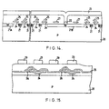
- Figure 13 is a plan view corresponding to the structure of the memory cell array circuit shown in Figure 12 when such a memory is actually provided on a semiconductor chip.
- Figure 14 is a cross-sectional view along the line I-I' in Figure 13.
- Figure 15 is a cross-sectional view along the line II-II' in Figure 13.
- Figure 16 is a cross-sectional view along the line III-III' in Figure 13.
- a P-type silicon semiconductor substrate is used as the substrate 20 in the memory of this embodiment.
- N + region 21A serves as a ground line 13.
- Metal leads 23, made for example of aluminium, are connected to N + regions 21B through contact holes 22 and serve as the bit lines 12.
- Electrodes 24, made of a first polycrystalline silicon layer and put in a floating electrical state, are formed between adjacent N + regions 21, insulated therefrom by an insulating layer. Electrodes 24 are the floating gate electrodes of the various memory cells 11.
- Electrodes 25, made of a third polycrystalline silicon layer, are formed over the sets of electrodes 24 that are disposed horizontally in Figure 13, insulated therefrom by an insulating layer. Electrodes 25 are the control gate electrodes of the memory cell 11 and serve as the column lines 14. Electrodes 26, made of a second polycrystalline silicon layer, are formed between adjacent series circuits disposed in different columns, and partially overlap electrodes 24, insulated therefrom by an insulating layer. Electrodes 26 are the common erase gate electrodes of the various memory cells 11 in the series circuit units.
- N + regions 21C are formed between adjacent N + regions 21B.
- a pair of N + regions 21D are also formed separate from N + regions 21C.
- N + regions 21C and 21D are the source and drain regions of switching transistor 16. Electrodes 27, made of the third polycrystalline silicon layer, are formed between these source and drain regions, insulated therefrom by an insulating layer. Electrodes 27 are the control gate electrodes of transistors 16 and serve as the erase selection lines 17. Electrodes 26, the common erase gate electrodes, are connected to N + regions 21D via a direct contact portion and metal leads 29, of, for example, aluminum, are connected to N + regions 21C via contact holes 28. Metal leads 29 serve as erase lines 15.
- the memory is a matrix of series circuit units 10, each of which comprises eight series connected memory cells 11. One end each of each series circuit unit 10 is connected to a bit line 12, embodied in metal lead 23, and the other end is connected to a ground line 13, embodied in N + region 21A.
- the control gate electrodes of the various memory cells 11 are connected to row lines 14, embodied in electrodes 25.
- the erase gate electrodes of each memory cell in a series circuit unit are commonly connected and coupled to erase lines 15 via transistors 16. The conduction of transistors 16 is controlled by signals from the corresponding erase selection line 17.
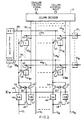
- Figure 1 is a diagram showing the overall configuration of an E 2 PROM according to one embodiment of the present invention.
- N bit lines 12 and N erase lines 15 are coupled to column decoder/input-output circuit 30 to which an erase control signal ER and a column address input are input. Parts of the row address inputs, discussed later, are input to column decoder/input-output circuit 30, and 8-bit input/output data is input to and output from circuit 30.
- the detailed configuration of column decoder/input-output circuit 30 will be described below.
- Eight row lines 14 are coupled to each of the series circuit unit selectors 31 1 to 31 M .
- Series circuit unit selectors 31 and M erase selection lines 17 are coupled to row decoder 32, to which row address input and erase control signal ER are input.
- Row decoder 32 outputs a selection signal to one series circuit unit selector 31 in response to a row address input, and selectively outputs a high voltage to one of M erase selection lines 17 in response to row address input during data erasure.
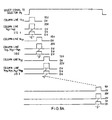
- Figure 2 is a circuit diagram showing the internal configuration of column decoder/input-output circuit 30.
- reference numeral 35 denotes a column decoder to which a column address input and an erase control signal ER are input.
- Erase lines 15 1 to 15 N and control lines 36 1 to 36 N are coupled to column decoder 35.
- Column decoder 35 selects one of control lines 36 1 to 36 N in response to the column address input during data writing and data reading and outputs a high voltage thereto.
- Decoder 35 selects one of erase lines 15 1 to 15 N during data erasure and similarly outputs a high voltage thereto.
- Reference numeral 37 denotes a selector, to which parts of the row address inputs (e.g., 3-bit addresses A 1 , A 2 , A 3 ) are input.
- Selector 37 has eight partial selectors RD1 - RD8 and selects one of control lines 38 1 to 38 N according to an input address, setting it to a high potential.
- Reference numerals 39 1 to 39 N denote first data lines
- reference numerals 40 1 to 40 8 denote second data lines.
- Latch circuits 41 11 ,.., 41 1N to 41 81 ,.., 41 8N for latching 1-bit data are provided at the respective intersections of the first and second data lines.
- the eight latch circuits disposed in a given column are coupled to the same first data line 39 through respective data transfer MOS transistors 42, a single transistor 42 being associated with each latch circuit 41.
- the N latch circuits disposed in a given row are coupled to the same second data line 40 through respective data transfer MOS transistors 43, a single transistor 43 being associated with each latch circuit 41.
- the gates of the N transistors 42 disposed in the same row are coupled to the corresponding one of control lines 38 1 to 38 8 and the gates of the eight transistors 43 disposed in the same column are coupled to the corresponding one of control lines 36 1 to 36 N .
- each first data line 39 Associated with each first data line 39 are two additional data transfer MOS transistors 44, 45. One terminal of both transistors 44, 45 is coupled to the associated data line 39. The remaining terminal of transistor 44 is coupled to the corresponding one of the bit lines 12 1 to 12 N through a sense amplifier 46 while the remaining terminal of transistor 45 is coupled to the corresponding bit line through data input buffer (DB) 47 and data transfer MOS transistor 48, respectively.
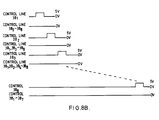
- the gates of MOS transistors 45, 48 are coupled to control line 49, to which a read/write control signal R/W, set to a low potential during data reading and to a high potential during data writing, is applied.
- the gates of MOS transistors 44 are coupled to control line 49 through inverters 50, respectively.
- Data input/output circuits (I/01 to I/08) 51 1 to 51 8 are coupled to second data lines 40 1 to 40 8 , respectively.
- each of the N bit lines 12 eight latch circuits 41 are provided for each of the N bit lines 12.
- the MOS transistors are all N-type.
- FIG. 3 is a circuit diagram showing the detailed configuration of a latch circuit 41 schematically shown in Figure 2.
- Latch circuit 41 is formed by cross-connecting the input and the output terminals of two CMOS inverters 55 and 56, each inverter having P-type and N-type MOS transistors.
- One terminal of the data transfer MOS transistors 42 is coupled to the output terminal of inverters 55 and one terminal of data transfer MOS transistors 43 is coupled to the output terminal of inverters 56.
- FIG 4 is a circuit diagram showing the detailed configuration of sense amplifier 46 schematically shown in Figure 2.
- Sense amplifier 46 may be activated by a chip enable control signal CE and includes a CMOS inverter 63 having a P-type MOS transistor 61 and an N-type MOS transistor 62 arranged such that the input and output terminals of the inverter are shortcircuited.
- P-type MOS transistor 64 is coupled between inverter 63 and power source Vcc and chip enable control signal CE is input to the gate thereof.
- N-channel MOS transistor 65 is coupled between the output terminal of CMOS inverter 63 and reference power source Vss and chip enable control signal CE is input to the gate thereof.
- P-type MOS transistor 66 is coupled between the output of CMOS inverter 63 and a junction between inverter 63 and MOS transistor 64.
- Two CMOS inverters 67, 68 are coupled in cascade to the output of inverter 63.
- the output of inverter 68 is transmitted as a sense amplifier output to corresponding data line 39 through MOS transistor 44 ( Figure 2), and is also fed back to the gate of MOS transistor 66.
- the sense amplifier configured as described above is activated in such a manner that transistor 64 is turned on and transistor 65 is turned off when chip enable control signal CE is set to a low-level potential in order to amplify the potential of co-responding bit line 12. Since the input and output terminals of CMOS inverter 63 are shortcircuited, its input terminal potential, i.e., the bit line potential is set, for example, to 1 V when Vcc is, for example, 5 V.
- FIG. 5 is a circuit diagram showing the detailed configuration of the data input buffer 47 schematically shown in Figure 2.
- Data input buffer 47 includes a CMOS inverter 71 and a depression type N-type MOS transistor 72, the first terminal of which is coupled to the output terminal of inverter 71.
- the voltage Vcc is applied to the gate of transistor 72.
- Two N-type MOS transistors 73, 74 are coupled in series between the second terminal of MOS transistor 72 and power source Vcc.
- N-type MOS transistor 75 is arranged such that its source and drain terminals are coupled together.
- a pulse signal 0 is input thereto to substantially produce a capacitor-like operation.
- the gates of transistors 73 and 75 are coupled to a junction between series-coupled transistors 73 and 74.
- the gate of transistor 74 is connected to the second terminal of MOS transistor 72.
- the data input buffer constructed as described above has a voltage rising function using a pulse signal.
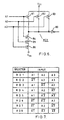
- FIG. 6 is a circuit diagram showing the detailed configuration of partial selector RD1 of the 8 partial selectors of selector 37 schematically shown in Figure 2.
- Partial selector RD1 has three P-type MOS transistors 81, 82, 83 coupled in parallel between power source Vcc and the input terminal of inverter 80.
- Three N-type MOS transistors 84, 85, 86 are coupled in series between the input terminal of inverter 80 and reference power source Vss.
- Bit A1 of the 3-bit row address input is input to the gates of transistors 81 and 84, A2 is input to the gates of transistors 82 and 85, and A3 is input to the gates of transistors 83 and 86.
- partial selector RD1 constructed as described above, when the 3-bit address inputs A1, A2, A3 are all set to a high potential and the three N-type MOS transistors 84, 85, 86 are all turned on, the input terminal of inverter 80 is discharged to Vss. Thus, the output signal of inverter 80 becomes high level, thereby selecting the corresponding control line 38.
- Figure 7 illustrates the address inputs of the eight partial selectors RD1 to RD8.
- Data is written by selecting one series circuit unit 10 and sequentially writing the data in the eight cells of the selected series circuit unit.
- Each cell of the selected series circuit unit is sequentially processed with a potential difference of 15 V imposed on the row line coupled to the control gate electrode of the cell being processed and a potential difference of 20 V imposed on the seven remaining row lines.
- the selected series circuit unit is coupled to bit line 12 1 and the eight row lines 14 11 to 14 81 .
- a selection signal is output from row decoder 32 to series circuit selector 31 1 , thereby selecting series circuit selector 31 1 .
- a selection signal is output from column decoder 35 in column decoder/input-output circuit 30 to control line 36 1 , and the eight transistors 43 whose gates are coupled to control line 36 1 are turned on. Then, data from second data lines 40 1 to 40 8 may be input to the eight latch circuits 41 11 to 41 81 disposed as shown in Figure 2.
- write data input from data input/output circuit 51 1 is transmitted to first data line 39 1 through second data line 40 1 , transistor 43, latch circuit 41 11 and transistor 42.
- signal R/W of control line 49 is set to a high potential during data writing, and thus transistors 45 and 48 are turned on.
- Write data transmitted to data line 39 1 may then be output to bit line 12 1 through data input buffer 47.
- the voltage of bit line 12 is maintained at one of two different voltages by the data input buffer 47 shown in Figure 5 in accordance with the data being written. When high-level data is written, it may be set to 10 V, for example, while when low-level data is written, it may be set to 0 V. At this time, all other bit lines are maintained at 0 V.
- the seven memory cells 11 whose control gate electrodes are supplied with the voltage of 20 V operate as triodes (non-saturation operation). In this operation a channel region is formed between the source and drain regions, as shown in Figure 17.
- bit line 12 1 and ground line 13 1 The voltage between bit line 12 1 and ground line 13 1 is imposed across the source and drain of the selected cell, connected to column line 14 11 . If bit line 12 1 is maintained at 10 V , electrons travel from the selected cell's source region to its drain region. A concentrated electric field, particularly in the depletion layer formed in the vicinity of the drain region, accelerates the electrons and imparts to them sufficient energy to cross the energy barrier of the insulating film from the surface of substrate 20, as shown in Figure 18. These electrons are called “hot electrons” and they are drawn to the selected cell's control gate electrode, which is set at the high voltage of 15 V . These hot electrons jump to and are captured by the floating gate electrode. As a result, the floating gate electrode of the selected cell becomes negatively charge and the threshold voltage rises to a high value.
- bit line 12 1 If a voltage of 0 V is applied to bit line 12 1 , the hot electrons are not generated and the threshold voltage remains in its original low state. Data may be written one cell at a time in this manner.
- output from series circuit selector 31 causes a voltage of 15 V to be imposed on row line 14 21 and a voltage of 20 V to be imposed on the seven remaining row lines.
- output from selector 37 causes a voltage of 5 V to be imposed on control line 38 2 and 0 V to be imposed on the seven remaining control lines.
- the transistor 42 whose gate is coupled to control line 38 2 is turned on, and the data latched in latch circuit 41 21 may be output to first data line 39 1 .
- data input from data input/output circuit 51 2 (I/02) is transmitted to first data line 39 1 through second data line 40 2 , transistor 43, latch circuit 41 21 and transistor 42.
- data may be written to the memory cell connected to row line 14 21 .
- data may be sequentially written to each of the remaining cells 11 in the selected series circuit unit 10.
- the selected series circuit units are coupled to the eight row lines 14 11 to 14 81 .
- a voltage of 2 V is initially applied only to row line 14 11
- a voltage of 7 V is applied to the seven remaining row lines 14 21 to 14 81 .
- the threshold voltages of the selected memory cells 11 have been set in accordance with the data written to them during the data writing operation.
- the voltage of 2 V is, for example, higher than the low threshold voltage of those cells which have had data erased and lower than the high threshold voltage after high-level data is written.
- the voltage of 7 V is sufficiently higher than the high threshold voltage after high-level data is written.
- applying the described voltages to the eight row lines 14 11 to 14 81 has the effect of turning on the memory cells whose control gate electrodes are coupled to the potential difference of 7 V, namely those cells on row lines 14 21 - 81 .
- the ON or OFF state of the selected cells whose control gate electrodes are coupled to column line 14 11 is determined by their threshold voltage, which as noted above, is set during the data write mode.
- Sense amplifier 46 coupled to bit lines 12 1 to 12 N is activated during data reading, and the potential of the corresponding bit line 12 is set to the reading voltage, for example, of 1 V by sense amplifier 46.
- Cells in the row of memory cells which is being processed that have a low threshold voltage i.e. have low-level data written therein
- the read voltage of the corresponding bit line 12 will be discharged to ground level line 13, through the corresponding series circuit unit.
- the cell has a high threshold voltage (i.e. has a high-level data written therein)
- it will remain off despite the imposition of the voltage of row lines 14 11 and the read voltage of the corresponding bit line 12 will not be discharged through the corresponding series circuit unit.
- the voltages of the N bit lines 12 1 to 12 N are dependent upon whether the threshold voltage of each of the selected cells is high or low, and amplification of these potential differences by sense amplifiers 46 makes it possible to determine whether high or low-level data is present on the associated bit line. Since signal R/W of signal line 49 is set to a low potential during data reading, the transistors 44 of Figure 2 are turned on. Thus, the reading data is amplified by sense amplifier 46 and then transmitted in parallel to the N first data lines 39 1 to 39 N .
- a voltage of 2 V is applied to row line 14 21 and a voltage of 7 V is applied to the remaining seven row lines.
- data may be read from the N cells coupled to row line 14 21 in a manner similar to that described above, amplified by sense amplifiers 46, determined to be high- or low-level data, and transmitted to data lines 39 1 to 39 N respectively.
- selector 37 Under the control of selector 37, a voltage of 5 V is applied to control line 38 2 and O V is applied to the seven remaining control lines.
- transistors 42 whose gates are coupled to control line 38 2 (maintained at 5 V), are turned on, and the data transmitted to the first data lines 39 1 to 39 N is latched in parallel in the N latch circuits 41 21 to 41 2N disposed in the same row.
- data is sequentially read from the cells 11 in similarly processed N series circuit units 10, and transferred to latch circuits 41.
- a selection signal is output to control line 36 1 by the output of decoder 35, and the eight transistors 43, whose gates are coupled to control line 36 1 , are turned on.
- the data latched in latch circuits 41 11 to 41 81 disposed as shown in Figure 2, are output in parallel to the eight second data lines 40 1 to 40 8 , and output externally in parallel through data input/output circuits 51 1 to 51 8 (I/01 to I/08).
- the selection signal is output to control line 36 2 , and transistors 43, whose gates are coupled to control line 36 2 , are turned on.
- the data latched in latch circuits 41 12 to 41 82 disposed as shown in Figure 2 is output in parallel to second data lines 40 1 to 40 8 , and output externally in parallel through data input/output circuits 51 1 to 51 8 (I/01 to I/08).
- data stored in the memory cells is sequentially output in eight bit (1 byte) units.
- Data may be read out in parallel from N series circuit units 10 during data reading.
- the reading time required when the data is read into latch circuits 41 from series circuit units 10 according to the present invention can be shortened by a factor of 1/N a compared with the memory of the prior art.
- the overall data reading rate can be accelerated.
- Each row line 14 and bit line 12 is maintained at 0 V during data erasure.
- a high voltage of 30 V is applied to the erase selecting line 17 coupled to the series circuit unit 10 to be erased.
- a high voltage of 25 V is applied to erase line 15 coupled to the series circuit unit 10 to be erased.
- the series circuit unit 10 to be erased is coupled to bit line 12 1 and the eight row lines 14 11 to 14 81 .
- the transistors 16 coupled to the series circuit units 10 disposed in the same row containing the series circuit unit to be erased are turned on.
- the high voltage of erase line 15, however, is applied only to the common erase gate electrode of the series circuit unit 10 coupled to erase line 15, which is maintained at the high voltage of 25 V.
- an electric field emission occurs between the floating gate and erase gate electrodes of the eight cells 11 in the selected series circuit unit 10, and electrons stored in the floating gate electrodes are discharged to the erase gate electrodes. Consequently, the threshold voltages of the cells return to a low-level state, and eight bits of data are erased, i.e., byte erasure is effected.
- row decoder 32 and column decoder 35 may be configured so that a high voltage of 30 V is applied to each erase selecting line 17 and a high voltage of 25 V is applied to each erase line 15. Data may also be erased in bit line units.
- the memory of the above-described embodiment permits reading and writing of data in units of 8 bits (1 byte) and electrical data erasure in byte units. Furthermore, one can look to large-scale integration, since the memory cell array includes only one non-volatile transistor for each memory cell. In contrast, conventional memories which permit electrical data erasure in byte units require each bit to comprise two or four transistors and are therefore unable to increase cell integration density. It is only possible to achieve a memory capacity of around 256 K bits in such a conventional memory. With the embodiment described above, however, since 1 bit comprises 1 transistor, it is possible to produce a memory with a degree of integration that is the same or better than that of the block erasure type memory illustrated in Figure 11.
- the above-described embodiment requires the provision of one switching transistor for every eight memory cells 11 and therefore needs 1.125 transistors per bit, or 0.125 more transistors per bit than the memory of Figure 11.
- the block erasure type memory of Figure 11 requires formation of a contact for each bit, in order to connect cells to corresponding bit lines.
- the memory of the present embodiment only needs one contact for every eight cells and so permits an improvement in the degree of integration.
- This invention is not limited to the embodiment described above but may be modified in a variety of ways.
- description was given above with reference to the case where data erasure is effected in byte units, it is also possible to effect block erasure of data from all cells, as in conventional memories, by the simultaneous imposition of a voltage of 30 V on all the erase selection lines 17 and a voltage of 25 V on all the erase lines 15 in data erasure.
- electrodes 25 in Figure 13 that are used as cell control electrodes and column lines 14 were described as being made of polycrystalline silicon, they may also be made of a high melting point metal silicide, such as titanium silicide or molybdenum silicide, etc., or by another high melting point metal.
- a memory cell array may be comprised of memory cells which comprise a single nonvolatile transistor, latch circuits 41 for use in reading data in parallel may be as many as N x 8, and those for an overhead may be extremely less as compared with the memory array section.
- the circuit of the memory of this embodiment the memory cells can be highly integrated.
Landscapes
- Engineering & Computer Science (AREA)
- Microelectronics & Electronic Packaging (AREA)
- Read Only Memory (AREA)
Claims (14)
- Dispositif pour lire des données ou pour écrire des données dans un ensemble d'unités de circuit (10), chaque unité de circuit (10) ayant une fonction d'enregistrement, desdites unités de circuit (10) étant disposées en une première matrice comprenant un ensemble de rangées et de colonnes, le dispositif comprenant:un ensemble de cellules d'enregistrement temporaire (41); etdes moyens de commande (37, 42, 44, 48) pour adresser les cellules d'enregistrement temporaire (41) et les unités de circuit (10), et pour commander le transfert de données sur des lignes de données (12) entre les cellules d'enregistrement temporaire (41) et les unités de circuit (10),caractérisé en ce que chacune desdites unités de circuit (10) comprend un ensemble de cellules de mémoire (11) connectées en série, et en ce que les cellules d'enregistrement temporaire (41) sont disposées en une seconde matrice comprenant un ensemble de rangées et de colonnes;lesdites lignes de données comprenant un ensemble de premières lignes de données (12), une seule desdites premières lignes de données (12) couplant les cellules d'enregistrement temporaire (41) dans une colonne donnée de la seconde matrice aux unités de circuit (10) dans une colonne donnée de la première matrice; etles moyens de commande comprenant un sélecteur d'adresse (31, 32, 35, 37, 42) comprenant des moyens pour adresser séquentiellement les cellules de mémoire (11) dans une unité de circuit sélectionnée (10), sous la dépendance de données d'adresse, de façon à transférer des données entre les cellules de mémoire (11) dans l'unité de circuit (10) sélectionnée et les cellules d'enregistrement temporaire (41) associées, de manière séquentielle, sur la première ligne de données (12) correspondante.
- Dispositif selon la revendication 1, comprenant des seconds moyens de commande (35, 43) pour commander le transfert de données entre les cellules d'enregistrement temporaire (41) et des moyens d'entrée/sortie (51) pour introduire des données dans le dispositif et pour émettre des données à partir de celui-ci.
- Dispositif selon la revendication 1, dans lequel les moyens de commande pour adresser séquentiellement l'ensemble de cellules de mémoire comprennent:
un ensemble de premiers moyens de commutation (42), un seul desdits premiers moyens de commutation (42) étant couplé entre l'une desdites cellules d'enregistrement temporaire (41) et la première ligne de données (12) correspondante, le premier moyen de commutation (42) qui est associé à une colonne donnée de cellules d'enregistrement temporaire (41) dans la seconde matrice étant activé selon une séquence prédéterminée conformément à des données d'adresse, de façon à effectuer le transfert séquentiel de données entre les cellules de mémoire (11) dans une unité de circuit (10) donnée, et la colonne donnée de cellules d'enregistrement temporaire (41). - Dispositif selon la revendication 1, comprenant en outre:
un ensemble de moyens amplificateurs de lecture (46), un seul desdits moyens amplificateurs de lecture (46) étant couplé à l'une desdites premières lignes de données (12) et étant adapté pour amplifier une tension maintenue sur ladite première ligne de données (12), de façon à effectuer la lecture de données dans les cellules de mémoire (11) d'une unité de circuit (10) qui est couplée à ladite première ligne de données (12). - Dispositif selon la revendication 1, comprenant en outre:
un ensemble de moyens amplificateurs-séparateurs de données (47), un seul desdits moyens amplificateurs-séparateurs de données (47) étant couplé à l'une desdites premières lignes de données (12) et adapté de façon à maintenir des tensions prédéterminées sur ladite première ligne de données (12), pour effectuer l'écriture de données dans les cellules de mémoire (11) d'une unité de circuit (10) qui est couplée à ladite première ligne de données. - Dispositif selon la revendication 1, comprenant en outre:
un ensemble de secondes lignes de données (40), une seule desdites secondes lignes de données (40) couplant les cellules d'enregistrement temporaire (41) dans une rangée donnée de la seconde matrice à des moyens d'entrée/sortie (51) pour introduire des données dans le dispositif et pour émettre des données à partir de celui-ci. - Dispositif selon la revendication 6, comprenant en outre:
un ensemble de seconds moyens de commutation (43), un seul desdits seconds moyens de commutation (43) étant couplé entre l'une desdites cellules d'enregistrement temporaire (41) et la seconde ligne de données (40) correspondante, les seconds moyens de commutation (43) étant activés d'une manière prédéterminée de façon à effectuer le transfert de données entre les cellules d'enregistrement temporaire (41) et les moyens d'entrée/sortie (51). - Dispositif selon l'une quelconque des revendications précédentes, dans lequel les cellules d'enregistrement temporaire comprennent des circuits de bascule.
- Dispositif selon la revendication 1, dans lequel le nombre de cellules d'enregistrement temporaire dans chaque colonne de la seconde matrice est égal au nombre de cellules de mémoire dans une unité de circuit.
- Dispositif selon l'une quelconque des revendications précédentes, dans lequel chaque cellule de mémoire (11) comprend un transistor non volatil programmable de façon électrique.
- Mémoire à semiconducteurs programmable comprenant un ensemble d'unités de circuit (10), comprenant chacune un ensemble de cellules de mémoire (11) connectées en série, et un dispositif selon l'une quelconque des revendications précédentes connecté à celles-ci, pour lire ou écrire des données dans les cellules de mémoire.
- Procédé de lecture de données ou d'écriture de données dans une unité de circuit (10) comprenant au moins deux cellules de mémoire (11) connectées en série, en utilisant un dispositif selon l'une quelconque des revendications précédentes, ce procédé comprenant les étapes suivantes:
on adresse séquentiellement chaque cellule de mémoire (11) dans l'unité de circuit, de façon à mémoriser séquentiellement dans l'une correspondante des cellules d'enregistrement temporaire des données qui sont enregistrées dans chaque cellule de mémoire; et on émet ou on introduit en parallèle les données mémorisées. - Procédé de lecture de données ou d'écriture de données dans un ensemble d'unités de circuit (10), chaque unité de circuit comprenant au moins deux cellules de mémoire (11) connectées en série, en utilisant un dispositif selon l'une quelconque des revendications 1 à 11, ce procédé comprenant les étapes suivantes: on adresse au moins une cellule de mémoire (11) dans chaque unité de l'ensemble d'unités de circuit; et on transfère simultanément des données enregistrées dans les cellules de mémoire adressées, dans chaque unité de circuit, vers des cellules d'enregistrement temporaire respectives qui leur sont associées.
- Procédé selon la revendication 13, comprenant en outre l'étape suivante:
on transfère des données, en parallèle, vers un dispositif de sortie, à partir des cellules d'enregistrement temporaire qui sont associées à chaque unité de circuit.
Priority Applications (2)
| Application Number | Priority Date | Filing Date | Title |
|---|---|---|---|
| EP92201954A EP0508552B1 (fr) | 1988-10-24 | 1988-10-24 | Mémoire à semi-conducteurs programmable |
| DE19883856085 DE3856085T2 (de) | 1988-10-24 | 1988-10-24 | Programmierbarer Halbleiterspeicher |
Applications Claiming Priority (2)
| Application Number | Priority Date | Filing Date | Title |
|---|---|---|---|
| EP92201954A EP0508552B1 (fr) | 1988-10-24 | 1988-10-24 | Mémoire à semi-conducteurs programmable |
| EP88309994A EP0365720B1 (fr) | 1988-10-24 | 1988-10-24 | Mémoire à semi-conducteurs programmable |
Related Parent Applications (1)
| Application Number | Title | Priority Date | Filing Date |
|---|---|---|---|
| EP88309994.7 Division | 1988-10-24 |
Publications (3)
| Publication Number | Publication Date |
|---|---|
| EP0508552A2 EP0508552A2 (fr) | 1992-10-14 |
| EP0508552A3 EP0508552A3 (en) | 1993-02-24 |
| EP0508552B1 true EP0508552B1 (fr) | 1997-12-10 |
Family
ID=8200258
Family Applications (2)
| Application Number | Title | Priority Date | Filing Date |
|---|---|---|---|
| EP88309994A Expired - Lifetime EP0365720B1 (fr) | 1988-10-24 | 1988-10-24 | Mémoire à semi-conducteurs programmable |
| EP92201954A Expired - Lifetime EP0508552B1 (fr) | 1988-10-24 | 1988-10-24 | Mémoire à semi-conducteurs programmable |
Family Applications Before (1)
| Application Number | Title | Priority Date | Filing Date |
|---|---|---|---|
| EP88309994A Expired - Lifetime EP0365720B1 (fr) | 1988-10-24 | 1988-10-24 | Mémoire à semi-conducteurs programmable |
Country Status (2)
| Country | Link |
|---|---|
| EP (2) | EP0365720B1 (fr) |
| DE (1) | DE3855180T2 (fr) |
Families Citing this family (7)
| Publication number | Priority date | Publication date | Assignee | Title |
|---|---|---|---|---|
| JPH07122989B2 (ja) * | 1990-06-27 | 1995-12-25 | 株式会社東芝 | 半導体記憶装置 |
| JP3060680B2 (ja) * | 1990-11-30 | 2000-07-10 | 日本電気株式会社 | 不揮発性半導体記憶装置 |
| JP2564046B2 (ja) * | 1991-02-13 | 1996-12-18 | 株式会社東芝 | 半導体記憶装置 |
| JP3464803B2 (ja) * | 1991-11-27 | 2003-11-10 | 株式会社東芝 | 半導体メモリセル |
| US5544103A (en) * | 1992-03-03 | 1996-08-06 | Xicor, Inc. | Compact page-erasable eeprom non-volatile memory |
| JP3450467B2 (ja) * | 1993-12-27 | 2003-09-22 | 株式会社東芝 | 不揮発性半導体記憶装置及びその製造方法 |
| JP3859766B2 (ja) * | 1996-05-24 | 2006-12-20 | 株式会社ルネサステクノロジ | 半導体記憶装置の入力回路 |
Family Cites Families (5)
| Publication number | Priority date | Publication date | Assignee | Title |
|---|---|---|---|---|
| US4485349A (en) * | 1983-04-08 | 1984-11-27 | Varian Associates, Inc. | Stabilized microwave power amplifier system |
| US4648074A (en) * | 1984-06-29 | 1987-03-03 | Rca Corporation | Reference circuit with semiconductor memory array |
| DE3586523T2 (de) * | 1984-10-17 | 1993-01-07 | Fujitsu Ltd | Halbleiterspeicheranordnung mit einer seriellen dateneingangs- und ausgangsschaltung. |
| JPH0827725B2 (ja) * | 1987-03-17 | 1996-03-21 | 富士通株式会社 | レジスタ回路 |
| JP2647101B2 (ja) * | 1987-11-17 | 1997-08-27 | 株式会社東芝 | 不揮発性半導体メモリ装置 |
-
1988
- 1988-10-24 DE DE19883855180 patent/DE3855180T2/de not_active Expired - Lifetime
- 1988-10-24 EP EP88309994A patent/EP0365720B1/fr not_active Expired - Lifetime
- 1988-10-24 EP EP92201954A patent/EP0508552B1/fr not_active Expired - Lifetime
Also Published As
| Publication number | Publication date |
|---|---|
| EP0508552A3 (en) | 1993-02-24 |
| EP0365720B1 (fr) | 1996-04-03 |
| EP0365720A1 (fr) | 1990-05-02 |
| EP0508552A2 (fr) | 1992-10-14 |
| DE3855180D1 (de) | 1996-05-09 |
| DE3855180T2 (de) | 1996-10-02 |
Similar Documents
| Publication | Publication Date | Title |
|---|---|---|
| KR100323970B1 (ko) | 비휘발성메모리구조 | |
| US6256231B1 (en) | EEPROM array using 2-bit non-volatile memory cells and method of implementing same | |
| US6181597B1 (en) | EEPROM array using 2-bit non-volatile memory cells with serial read operations | |
| US6081456A (en) | Bit line control circuit for a memory array using 2-bit non-volatile memory cells | |
| US6157570A (en) | Program/erase endurance of EEPROM memory cells | |
| US5294819A (en) | Single-transistor cell EEPROM array for analog or digital storage | |
| US4543647A (en) | Electrically programmable non-volatile semiconductor memory device | |
| US6288941B1 (en) | Electrically erasable semiconductor non-volatile memory device having memory cell array divided into memory blocks | |
| US5812453A (en) | Programmable semiconductor memory | |
| US4527259A (en) | Semiconductor device having insulated gate type non-volatile semiconductor memory elements | |
| JPH0869696A (ja) | 半導体記憶装置 | |
| US4630087A (en) | Nonvolatile semiconductor memory device | |
| KR950011965B1 (ko) | 불휘발성 반도체 메모리 장치 | |
| EP0317324A2 (fr) | Mémoire semi-conductrice programmable | |
| EP1214715B1 (fr) | Cellule 1-transistor pour une application de memoire eeprom | |
| EP0508552B1 (fr) | Mémoire à semi-conducteurs programmable | |
| US5245566A (en) | Programmable semiconductor | |
| US4901285A (en) | High density read-only memory | |
| JPH0793985A (ja) | 半導体記憶装置及びそのデータ書込み方法 | |
| US20040156236A1 (en) | Programmable semiconductor memory | |
| JPH06103790A (ja) | 不揮発性半導体記憶装置 | |
| JPH0581194B2 (fr) | ||
| US6466479B2 (en) | Non-volatile memory matrix architecture with vertical insulation strips between adjacent memory blocks | |
| US5719805A (en) | Electrically programmable non-volatile semiconductor memory including series connected memory cells and decoder circuitry for applying a ground voltage to non-selected circuit units | |
| EP0365721B1 (fr) | Mémoire à semi-conducteur programmable |
Legal Events
| Date | Code | Title | Description |
|---|---|---|---|
| PUAI | Public reference made under article 153(3) epc to a published international application that has entered the european phase |
Free format text: ORIGINAL CODE: 0009012 |
|
| 17P | Request for examination filed |
Effective date: 19920720 |
|
| AC | Divisional application: reference to earlier application |
Ref document number: 365720 Country of ref document: EP |
|
| AK | Designated contracting states |
Kind code of ref document: A2 Designated state(s): DE FR GB |
|
| PUAL | Search report despatched |
Free format text: ORIGINAL CODE: 0009013 |
|
| AK | Designated contracting states |
Kind code of ref document: A3 Designated state(s): DE FR GB |
|
| 17Q | First examination report despatched |
Effective date: 19960528 |
|
| GRAG | Despatch of communication of intention to grant |
Free format text: ORIGINAL CODE: EPIDOS AGRA |
|
| GRAG | Despatch of communication of intention to grant |
Free format text: ORIGINAL CODE: EPIDOS AGRA |
|
| GRAH | Despatch of communication of intention to grant a patent |
Free format text: ORIGINAL CODE: EPIDOS IGRA |
|
| GRAH | Despatch of communication of intention to grant a patent |
Free format text: ORIGINAL CODE: EPIDOS IGRA |
|
| GRAA | (expected) grant |
Free format text: ORIGINAL CODE: 0009210 |
|
| AC | Divisional application: reference to earlier application |
Ref document number: 365720 Country of ref document: EP |
|
| AK | Designated contracting states |
Kind code of ref document: B1 Designated state(s): DE FR GB |
|
| REF | Corresponds to: |
Ref document number: 3856085 Country of ref document: DE Date of ref document: 19980122 |
|
| ET | Fr: translation filed | ||
| REG | Reference to a national code |
Ref country code: GB Ref legal event code: 746 Effective date: 19980910 |
|
| PLBE | No opposition filed within time limit |
Free format text: ORIGINAL CODE: 0009261 |
|
| STAA | Information on the status of an ep patent application or granted ep patent |
Free format text: STATUS: NO OPPOSITION FILED WITHIN TIME LIMIT |
|
| 26N | No opposition filed | ||
| REG | Reference to a national code |
Ref country code: FR Ref legal event code: D6 |
|
| REG | Reference to a national code |
Ref country code: GB Ref legal event code: IF02 |
|
| PGFP | Annual fee paid to national office [announced via postgrant information from national office to epo] |
Ref country code: DE Payment date: 20071018 Year of fee payment: 20 |
|
| PGFP | Annual fee paid to national office [announced via postgrant information from national office to epo] |
Ref country code: FR Payment date: 20071009 Year of fee payment: 20 Ref country code: GB Payment date: 20071024 Year of fee payment: 20 |
|
| REG | Reference to a national code |
Ref country code: GB Ref legal event code: PE20 Expiry date: 20081023 |
|
| PG25 | Lapsed in a contracting state [announced via postgrant information from national office to epo] |
Ref country code: GB Free format text: LAPSE BECAUSE OF EXPIRATION OF PROTECTION Effective date: 20081023 |