EP0508337A2 - Circuit inverseur pour une source de lumière capacitive - Google Patents
Circuit inverseur pour une source de lumière capacitive Download PDFInfo
- Publication number
- EP0508337A2 EP0508337A2 EP92105863A EP92105863A EP0508337A2 EP 0508337 A2 EP0508337 A2 EP 0508337A2 EP 92105863 A EP92105863 A EP 92105863A EP 92105863 A EP92105863 A EP 92105863A EP 0508337 A2 EP0508337 A2 EP 0508337A2
- Authority
- EP
- European Patent Office
- Prior art keywords
- inverter circuit
- light source
- voltage
- circuit according
- capacitance
- Prior art date
- Legal status (The legal status is an assumption and is not a legal conclusion. Google has not performed a legal analysis and makes no representation as to the accuracy of the status listed.)
- Withdrawn
Links
- 239000003990 capacitor Substances 0.000 claims abstract description 51
- 238000004804 winding Methods 0.000 claims description 29
- 238000000034 method Methods 0.000 claims description 13
- 230000008569 process Effects 0.000 claims description 13
- 230000001419 dependent effect Effects 0.000 claims description 3
- 230000010355 oscillation Effects 0.000 description 4
- 230000000903 blocking effect Effects 0.000 description 3
- 230000008901 benefit Effects 0.000 description 2
- 230000008859 change Effects 0.000 description 2
- 238000010586 diagram Methods 0.000 description 2
- XEEYBQQBJWHFJM-UHFFFAOYSA-N Iron Chemical group [Fe] XEEYBQQBJWHFJM-UHFFFAOYSA-N 0.000 description 1
- 230000009471 action Effects 0.000 description 1
- 238000013459 approach Methods 0.000 description 1
- 230000008878 coupling Effects 0.000 description 1
- 238000010168 coupling process Methods 0.000 description 1
- 238000005859 coupling reaction Methods 0.000 description 1
- 230000003247 decreasing effect Effects 0.000 description 1
- 230000000694 effects Effects 0.000 description 1
- 239000011888 foil Substances 0.000 description 1
- 230000001939 inductive effect Effects 0.000 description 1
Images


Classifications
-
- H—ELECTRICITY
- H05—ELECTRIC TECHNIQUES NOT OTHERWISE PROVIDED FOR
- H05B—ELECTRIC HEATING; ELECTRIC LIGHT SOURCES NOT OTHERWISE PROVIDED FOR; CIRCUIT ARRANGEMENTS FOR ELECTRIC LIGHT SOURCES, IN GENERAL
- H05B44/00—Circuit arrangements for operating electroluminescent light sources
-
- H—ELECTRICITY
- H05—ELECTRIC TECHNIQUES NOT OTHERWISE PROVIDED FOR
- H05B—ELECTRIC HEATING; ELECTRIC LIGHT SOURCES NOT OTHERWISE PROVIDED FOR; CIRCUIT ARRANGEMENTS FOR ELECTRIC LIGHT SOURCES, IN GENERAL
- H05B47/00—Circuit arrangements for operating light sources in general, i.e. where the type of light source is not relevant
- H05B47/10—Controlling the light source
Definitions
- the invention relates to an inverter circuit for the operation of a capacitive light source, in particular electroluminescent film, for example for aviation devices, the inverter circuit being connected to a direct current source and generating an alternating voltage for the light source.
- Electroluminescent films for lighting purposes are known on the market. For example, they can be used as emergency lighting in aircraft. Such electroluminescent foils are very capacitive. Their active current is in a ratio of, for example, 1 to 6.3 to their reactive current. The AC voltage required for their operation is usually less than 200 V, with operating frequencies between 50 Hz and 5 kHz.
- Aircraft usually work to supply emergency lighting with a DC power source that has, for example, a nominal voltage of 60V.
- the object of the invention is to propose an inverter circuit with which a strongly capacitive light source with the necessary operating alternating voltage and operating frequency can be fed from a direct current source.
- the above object is achieved in an inverter circuit of the type mentioned in that a coil arrangement is connected to the capacitance of the light source, that a first is connected to the coil arrangement and a second circuit branch, that in each of the two circuit branches a switch and a charging capacitor are connected in series, which is kept positively charged by the direct current source in the first circuit branch and negatively charged in the second circuit branch, and that a control circuit periodically switches the two switches alternately on , whereby the capacity of the light source is recharged via the coil arrangement and recharged from the respective charging capacitor.
- this inverter circuit is capable of receiving or temporarily storing the comparatively large capacitive reactive power of the light source during the recharging process of the capacity of the light source, without the reactive power having to be fed back into the direct current source.
- the inverter circuit has the further advantage that it can be constructed with simple and robust components.
- the coil arrangement can be constructed comparatively easily and small, since its inductance can be small. This is possible because it has been found that the light source does not have to be operated with a sinusoidal AC voltage, but can also be operated with an approximately rectangular or trapezoidal AC voltage. This makes it possible to carry out the recharging process quickly in comparison to the period of the AC voltage. This allows the use of comparatively small inductors.
- the frequency of the recharging process can be substantially greater than the operating frequency.
- the permissible level of the frequency of the reloading process in aircraft is restricted by regulations. These regulations serve to limit interference frequencies in the aircraft.
- the frequency of the reloading process can, however, also be reduced to the operating frequency.
- the curve shape then changes continuously from the rectangular shape to the sinus shape. This increases the size of the inductance.
- a certain electroluminescent film (1) can be represented electrically approximately by an equivalent circuit diagram consisting of a capacitor (C) and an ohmic resistor (R), cos phi at 400 Hz being approximately 0.16.
- the reactive current is therefore comparatively high compared to the active current.
- a direct current source (G1) and a reversely polarized direct current source (G2) are provided for feeding the electroluminescent film (1).
- a single direct current source (G) is sufficient.
- the capacitance (C) of the electroluminescent film (1) lies on a coil arrangement (2).
- this is formed by windings (L1, L2) with an iron core connected in series.
- the capacitance (C) lies at the center tap (3) of the windings.
- the inductances of the two windings (L1, L2) are essentially the same size.
- a first circuit branch (4) is connected to the winding (L1).
- a second circuit branch (5) is connected to the winding (L2).
- the series connection of the second circuit branch (5) and the winding (L2) is parallel to the capacitance (C).
- the first circuit branch (4) has a diode (D2), a charging capacitor (C1) and a switch (S1) in series connection.
- D2 Parallel to the partial series connection of the charging capacitor (C1) and the diode (D2) is a diode (D1) which is polarized like the diode (D2).
- a capacitor (CP1) is shown parallel to the diode (D1), which embodies the junction capacitance of the diodes (D1, D2).
- a series connection of a resistor (R1) and a capacitor (C3) is connected in parallel with the switch (S1).
- the second circuit branch (5) is constructed accordingly, but with reversed polarity.
- a diode (D5), a charging capacitor (C2) and a switch (S2) are connected in series to the winding (L2).
- a diode (D6) is connected in parallel with the partial series connection of the diode (D5) and the capacitor (C2).
- a junction capacitance (CP2) based on the diodes (D5, D6) is shown parallel to this.
- a series circuit consisting of a diode (D4) and the direct current source (G2) is connected in parallel with the charging capacitor (C2).
- D4 diode
- G2 direct current source
- C2 charging capacitor
- Parallel to the switch (S2) is a series circuit consisting of a resistor (R2) and a capacitor (C4).
- the switches (S1, S2) are electronic Switching elements, in particular thyristors, are formed. Triacs could also be provided instead.
- the thyristors or triacs have the advantage over transistors that are possible per se that they are easier to control here.
- the switches (S1, S2) are turned on by a control circuit (6) in the manner described in more detail below. This can be simply constructed since it does not have to switch the thyristors or triacs to the blocking state. The thyristors or triacs reach the blocking state in the manner described below.
- the switches (S1, S2) are grounded with one pole.
- the switches (S1) between the diodes (D2, D5) and the windings (L1 or L2), as shown in FIG. 2.
- the charging capacitors (C1, C2) are connected to ground here. These are kept in voltage by a single direct current source (G).
- the diode (D3) is sufficient.
- the diode (D4) can be omitted.
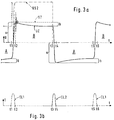
- the mode of operation of the inverter circuit described is essentially as follows (FIG. 3): At time (t1), the switch (S1) is turned on by the control circuit (6). Then the switch (S2) is locked at the latest. At time (t3), the switch (S2) is turned on by the control circuit (6). The switch (S1) is then blocked. At time (t5) the switch (S1) is turned on again. Then the switch (S2) is blocked.
- the intervals between the times (t1, t3 and t5) determine the operating frequency for the electroluminescent film (1). This is, for example, 400 Hz.
- the voltage (UC) across the capacitance (C) is shown in FIG. 3a, the negative half-periods of which are denoted by A and the positive half-periods of which are denoted by B.
- the voltage (U7) at point (7) is shown in dashed lines in Figure 3a, which lies at point (7) between the diode (D5) and the winding (L2).
- the voltage (U2) present at the switch (S2) is shown in dash-dot lines.
- FIG 3b is the current flowing through the winding (L2) (IL1) and the current (IL2) flowing through the winding (L2) are shown.
- the negative half-period (A) comes to an end.
- the capacitance (C) is still negatively charged.
- their voltage value has decreased by the value (b) due to the resistance (R) compared to their initial charging voltage (a).
- the value (b) is clearly small compared to the value (a).
- switch (S1) is switched on.
- the capacitor (C1) charged by the current source (G1) (FIG. 1) or (G) (FIG. 2) is connected to the winding (L1) via the diode (D2).
- the other, negative connection of the capacitor (C1) is connected to ground via the switch (S1).
- a current (IL1) begins to flow through the winding (L1).
- the shape of this current is that of a sine half wave.
- This current (IL1) partially discharges the capacitor (C1) and completely recharges the capacitance (C).
- the current (IL1) is in the form of a sine half-wave.
- the frequency of this current sine half-wave is significantly higher than the operating frequency.
- the frequency of this reloading process is, for example, 8 kHz.
- the voltage (UC) follows this. It has one between the times (t1 and t2) a curve corresponding to a sinusoidal oscillation, this sinusoidal oscillation running between the negative maximum and the positive maximum of a sinusoidal oscillation.
- the current (IL1) cannot become negative because the diodes (D1, D2) prevent a current reversal.
- the result of this is that the switch (S1), especially the thyristor, locks itself.
- the amount of voltage (UC) at time (t2) is equal to the voltage (UC) at time (t1) plus the voltage of the capacitor (C1) at time (t2).
- the capacitance (C) is thus charged in the positive direction at the time (t2) and at the same time increased by the voltage of the capacitor (C1) in the positive direction.
- the voltage (UC) across the capacitance (C) drops as a result of the resistance (R).
- the thyristor specially designed as switch (S1) locks after its release time.
- the voltage (UC) across the capacitance (C), as stated, is negative, so that the diodes (D5, D6) are blocked.
- the voltage across the winding (L2) is equal to the voltage across the winding (L1) due to the transformer coupling of the windings (L1, L2). This in turn is equal to the voltage across the capacitor (C) plus the voltage across the capacitor (C1).
- a capacitor (C5) with a voltage-dependent resistor (R3) connected in parallel is provided. This limits the maximum charge reversal voltage. If the load is suddenly reduced, the output voltage increases. The excess energy is absorbed by the voltage-dependent resistor (R3).
Landscapes
- Physics & Mathematics (AREA)
- Engineering & Computer Science (AREA)
- Microelectronics & Electronic Packaging (AREA)
- Optics & Photonics (AREA)
- Inverter Devices (AREA)
Applications Claiming Priority (2)
| Application Number | Priority Date | Filing Date | Title |
|---|---|---|---|
| DE4111581A DE4111581A1 (de) | 1991-04-10 | 1991-04-10 | Inverterschalter fuer eine kapazitive lichtquelle |
| DE4111581 | 1991-04-10 |
Publications (2)
| Publication Number | Publication Date |
|---|---|
| EP0508337A2 true EP0508337A2 (fr) | 1992-10-14 |
| EP0508337A3 EP0508337A3 (en) | 1993-02-03 |
Family
ID=6429211
Family Applications (1)
| Application Number | Title | Priority Date | Filing Date |
|---|---|---|---|
| EP19920105863 Withdrawn EP0508337A3 (en) | 1991-04-10 | 1992-04-04 | Inverter circuit for a capacitive light source |
Country Status (2)
| Country | Link |
|---|---|
| EP (1) | EP0508337A3 (fr) |
| DE (1) | DE4111581A1 (fr) |
Cited By (2)
| Publication number | Priority date | Publication date | Assignee | Title |
|---|---|---|---|---|
| EP0699015A1 (fr) * | 1994-08-24 | 1996-02-28 | Hewlett-Packard Company | Circuit d'alimentation à récupération de l'énergie pour un dispositif électroluminescent |
| WO1998057524A1 (fr) * | 1997-06-09 | 1998-12-17 | Telefonaktiebolaget Lm Ericsson | Circuit inverseur destine a allumer une lampe electroluminescente |
Family Cites Families (5)
| Publication number | Priority date | Publication date | Assignee | Title |
|---|---|---|---|---|
| US4070663A (en) * | 1975-07-07 | 1978-01-24 | Sharp Kabushiki Kaisha | Control system for driving a capacitive display unit such as an EL display panel |
| US4633141A (en) * | 1985-02-28 | 1986-12-30 | Motorola, Inc. | Low voltage power source power inverter for an electroluminescent drive |
| US5027040A (en) * | 1988-09-14 | 1991-06-25 | Daichi Company, Ltd. | EL operating power supply circuit |
| US5323305A (en) * | 1990-02-07 | 1994-06-21 | Daichi Co., Ltd. | Light emitting power supply circuit |
| JPH04233193A (ja) * | 1990-12-28 | 1992-08-21 | Stanley Electric Co Ltd | El素子駆動回路 |
-
1991
- 1991-04-10 DE DE4111581A patent/DE4111581A1/de active Granted
-
1992
- 1992-04-04 EP EP19920105863 patent/EP0508337A3/de not_active Withdrawn
Cited By (4)
| Publication number | Priority date | Publication date | Assignee | Title |
|---|---|---|---|---|
| EP0699015A1 (fr) * | 1994-08-24 | 1996-02-28 | Hewlett-Packard Company | Circuit d'alimentation à récupération de l'énergie pour un dispositif électroluminescent |
| US5559402A (en) * | 1994-08-24 | 1996-09-24 | Hewlett-Packard Company | Power circuit with energy recovery for driving an electroluminescent device |
| WO1998057524A1 (fr) * | 1997-06-09 | 1998-12-17 | Telefonaktiebolaget Lm Ericsson | Circuit inverseur destine a allumer une lampe electroluminescente |
| US6038153A (en) * | 1997-06-09 | 2000-03-14 | Telefonaktiebolaget Lm Ericsson | Inverter circuit for illuminating an electroluminescent lamp |
Also Published As
| Publication number | Publication date |
|---|---|
| DE4111581A1 (de) | 1992-10-15 |
| EP0508337A3 (en) | 1993-02-03 |
| DE4111581C2 (fr) | 1993-04-08 |
Similar Documents
| Publication | Publication Date | Title |
|---|---|---|
| DE19607704B4 (de) | Vorrichtung zur magnetischen Anregung von neuro-muskularem Gewebe | |
| EP2027647B1 (fr) | Dispositif d'alimentation électrique dans un réseau d'alimentation électrique et convertisseur de tension continue destiné à un tel dispositif | |
| DE19545154C2 (de) | Stromversorgungseinrichtung | |
| DE3785534T2 (de) | Parallel resonanter auf-abwaertskonverter. | |
| DE69118501T2 (de) | Wechselrichteranordnung | |
| EP0301436B1 (fr) | Convertisseur DC-DC | |
| DE2827693A1 (de) | Wechselrichter und dessen verwendung in einem batterieladegeraet | |
| DE60200710T2 (de) | Schaltnetzteil | |
| EP0772902B1 (fr) | Appareil d'alimentation en courant, notamment appareil de chargement de batteries pour vehicules electriques ou similaires | |
| DE3308407C2 (fr) | ||
| DE69410775T2 (de) | Elektronisches Vorschaltgerät für Entladungslampen mit einem Resonanzkreis zur Begrenzung des Formfaktors und zur Verbesserung des Leistungsfaktors | |
| DE1099062B (de) | Steuerbare Einrichtung zur Umformung von Gleichspannungen bzw. -stroemen in einer Brueckenschaltung | |
| DE2106310A1 (de) | Mehrphasen Leistungskonverterschaltung | |
| DE3014419A1 (de) | Vorschaltgeraet zum anschluss einer entladungslampe | |
| EP0057910B1 (fr) | Circuit pour l'alimentation régulée d'un utilisateur | |
| DE2802505A1 (de) | Roentgendiagnostikgenerator mit einem seinen hochspannungstransformator speisenden wechselrichter | |
| EP0135968B1 (fr) | Convertisseur de tension alternative | |
| DE2624123A1 (de) | Speiseschaltung fuer niederdruck- entladungslampen | |
| DE2537299C2 (de) | Serienschwingkreis-Wechselrichter | |
| DE4111581C2 (fr) | ||
| DE3714175C2 (fr) | ||
| DE1918183A1 (de) | Wechselrichter fuer induktive Verbraucher und Verwendung desselben als Frequenzwandler | |
| DE69205476T2 (de) | Verfahren und Vorrichtung zum Dämpfen des Funkstörungseffektes auf Leitern im mehrphasigen Wechselstromnetz. | |
| DE3519414C2 (de) | Transistorwechselrichterschaltung | |
| DE1488180A1 (de) | Wechselrichter fuer hoehere Frequenzen mit steuerbaren Gleichrichtern |
Legal Events
| Date | Code | Title | Description |
|---|---|---|---|
| PUAI | Public reference made under article 153(3) epc to a published international application that has entered the european phase |
Free format text: ORIGINAL CODE: 0009012 |
|
| AK | Designated contracting states |
Kind code of ref document: A2 Designated state(s): DE FR GB IT NL SE |
|
| PUAL | Search report despatched |
Free format text: ORIGINAL CODE: 0009013 |
|
| AK | Designated contracting states |
Kind code of ref document: A3 Designated state(s): DE FR GB IT NL SE |
|
| 17P | Request for examination filed |
Effective date: 19930107 |
|
| 17Q | First examination report despatched |
Effective date: 19941206 |
|
| GRAH | Despatch of communication of intention to grant a patent |
Free format text: ORIGINAL CODE: EPIDOS IGRA |
|
| STAA | Information on the status of an ep patent application or granted ep patent |
Free format text: STATUS: THE APPLICATION IS DEEMED TO BE WITHDRAWN |
|
| 18D | Application deemed to be withdrawn |
Effective date: 19961101 |