EP0505259A2 - Supraleitender Feldeffekttransistor und Verfahren zur Herstellung einer Mehrfachlagenstruktur für diesen Transistor - Google Patents
Supraleitender Feldeffekttransistor und Verfahren zur Herstellung einer Mehrfachlagenstruktur für diesen Transistor Download PDFInfo
- Publication number
- EP0505259A2 EP0505259A2 EP19920400697 EP92400697A EP0505259A2 EP 0505259 A2 EP0505259 A2 EP 0505259A2 EP 19920400697 EP19920400697 EP 19920400697 EP 92400697 A EP92400697 A EP 92400697A EP 0505259 A2 EP0505259 A2 EP 0505259A2
- Authority
- EP
- European Patent Office
- Prior art keywords
- superconductive
- layer
- thickness
- layers
- superconductive layer
- Prior art date
- Legal status (The legal status is an assumption and is not a legal conclusion. Google has not performed a legal analysis and makes no representation as to the accuracy of the status listed.)
- Granted
Links
Images
Classifications
-
- H—ELECTRICITY
- H10—SEMICONDUCTOR DEVICES; ELECTRIC SOLID-STATE DEVICES NOT OTHERWISE PROVIDED FOR
- H10N—ELECTRIC SOLID-STATE DEVICES NOT OTHERWISE PROVIDED FOR
- H10N60/00—Superconducting devices
- H10N60/80—Constructional details
- H10N60/85—Superconducting active materials
- H10N60/855—Ceramic superconductors
- H10N60/857—Ceramic superconductors comprising copper oxide
- H10N60/858—Ceramic superconductors comprising copper oxide having multilayered structures, e.g. superlattices
-
- H—ELECTRICITY
- H10—SEMICONDUCTOR DEVICES; ELECTRIC SOLID-STATE DEVICES NOT OTHERWISE PROVIDED FOR
- H10N—ELECTRIC SOLID-STATE DEVICES NOT OTHERWISE PROVIDED FOR
- H10N60/00—Superconducting devices
- H10N60/20—Permanent superconducting devices
- H10N60/205—Permanent superconducting devices having three or more electrodes, e.g. transistor-like structures
- H10N60/207—Field effect devices
Definitions
- the invention relates to a superconductive field effect transistor and to a method of manufacturing a multilayer structure such as that used in the transistor.
- HTSC High Temperature Super-Conductor
- oxide critical high temperature superconducting material
- FET superconductive field effect transistor
- the superconductive transistor is similar to a conventional field effect transistor and comprises, on the surface of a semiconductor substrate of InSb, InAs or InAsGa for example, an epitaxial semiconductor layer doped with n conductivity type serving as a support for source and drain superconductive electrodes delimiting in the epitaxial layer a channel covered by a gate insulation layer supporting the gate electrode.
- the source-drain distance which defines the electrical length of the transistor channel, corresponds substantially to the coherence length of the superconducting material so as to allow diffusion of Cooper pairs between the source and the drain by Josephson effect.
- the maximum superconductive current I o which can pass through a Josephson junction is inversely proportional to the resistance R n in the normal state of the barrier of the junction.
- the canal plays the role of this barrier.
- the channel epitaxial layer allows the proximity effect of the superconducting charge carriers to pass.
- the device therefore has a transistor effect.
- the second operating principle of a superconductive field effect transistor is illustrated for example in the Japanese patent application published under the number 01-155671.
- the transistor described therein is formed from a metal substrate.
- One face of the substrate carries a multilayer structure made of a dielectric layer covered with a superconductive layer defining a channel between the source and drain electrodes.
- the other side of the substrate carries a control electrode.
- the dielectric layer given as an example was made of oriented SrTiO3 (100) and 200 nm thick, or thick MgO of 150 nm.
- the superconductive layer belonged to the RE-Ba-Cu-O family and was 60 nm thick. In operation, the number of charge carriers which pass through the superconducting channel is adjusted by the electric field produced by the control voltage.
- This electric field causes an accumulation of charges at the interface of the superconductive layer with the dielectric layer and destroys electronic pairs in the superconductive layer. This destruction removes the superconductivity of the superconductive layer and therefore reduces the current flowing through it.
- the inventors claim to have observed such an effect in a transistor including a superconductive layer of YBa2Cu3O 6 + x separated, via a dielectric layer SrTiO3 thick of 200 nm, from a control electrode brought to a voltage of 450 V .
- the control voltage to be applied to the substrate of the transistor to obtain the desired field effect is very high (450 volts, in the example cited), incompatible with current applications of the transistors.
- the Japanese document reports the observation of a current between the source and the drain, without indicating the value. In reality, this current has a very low intensity.
- the superconductive layer carrying this current had a relatively high thickness (60 nm), as did the thickness of the underlying dielectric layer (150 or 200 nm depending on the material used). A decrease in the thickness of the superconductive layer suggests a decrease in the current, while experience shows that an increase in the thickness does not produce a significantly greater current.
- the aforementioned Japanese document gives no indication of the parameters determining the variation in the value of the field effect produced by the prior transistor. It therefore does not optimize the field effect.
- those skilled in the art could think of adjusting the number p of charge carriers in HTSC material.
- the concentration of charge carriers can in fact be adjusted by acting on the oxygen concentration in the HTSC material.
- the oxygen concentration is difficult to control.
- the invention remedies these drawbacks and presents a superconductive field effect transistor capable of conducting large currents, of a few mA for example, under a low drain-source voltage of the order of 10 mV for example, and under the control low voltage, only a few volts.
- the invention further presents a method for adjusting the number p of free carriers for optimizing the field effect.
- a field effect superconductive transistor comprising a substrate carrying a structure made of a non-superconductive layer covered with a superconductive layer defining a channel between source and drain electrodes, and a gate electrode, is characterized in that the gate electrode is arranged on the channel and the superconductive layer has a thickness of the order of magnitude of the Debye length, the structure being able to be repeated n times and being made so that the layers have continuous interfaces between them.
- the invention also relates to a method for manufacturing a multilayer structure such as that defined above, comprising at least one pair made of a non-superconductive layer covered with a superconductive layer, characterized in that it consists in adjusting the thickness of the layers of each pair so that the critical temperature T c varies greatly as a function of the number (p) of charge carriers in the superconductive layer in zero electric field and that the thickness of the non-superconductive layer allows reception optimal charge carriers provided by the superconductive layer.
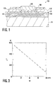
- the field effect superconductive transistor 10 has an insulated gate structure, for example of the MOS (Metal-Oxide-Semiconductor) type. It is formed on the surface of a substrate 11 and comprises a source electrode 12 and a drain electrode 13 resting on a structure constituting a current channel 14 between these two electrodes.
- the channel 14 carries a gate electrode 15 via a gate insulation film 16.
- the dimension ratios shown in Figure 1 have been intentionally modified for clarity of drawings.
- the transistor 10 has the substrate made of MgO, the source and drain electrodes 12, 13 and the grid 15 made of YBa2Cu3O7 superconductive material and the grid insulation film 16 in SiO2.
- the channel 14 is formed of a multilayer structure resting on the substrate 11.
- the channel structure 14 is made from a superconductive layer 17 and a non-superconductive layer 18.
- the pair of layers 17 and 18 is repeated three times in the channel structure 14. In each pair, the superconductive layer 17 is the upper layer.
- each superconductive layer 17 has a very small thickness, of the order of only a few nanometers. The inventors have attempted to explain this value by the following theory, which gives this thickness the order of magnitude of the Debye length L D.
- the critical temperature T c goes from 80K to 70K when the number p decreases from 0.16 to 0.13 charge carriers per group of Cu-O.
- the transition between the superconducting state and the normal state, caused by the application of an electric field, is due to the fact that the critical temperature T c of the zone depleted in carriers of load becomes lower than its zero field operating temperature. Under these conditions, the depth of penetration of the electric field into the channel could be roughly assessed in the following manner.
- the channel structure 14 of the transistor shown in FIG. 1 has been based on the article by JM Triscone et al in the journal Physical Review Letters, Vol. 64, No 7, Feb. 12, 1990, pages 804-807, entitled "YBa2Cu3O7 / PrBa2Cu3O7 Superlattices: Properties of Ultrathin Superconducting Layers Separated by Insulating Layers".
- the structure described is formed by a non-zero whole number of superimposed pairs, each composed of an upper superconductive layer 17 of YBa2Cu3O7 and a dielectric layer 18 of YBa2Cu3O7.
- the superconductive layer 17 of each pair had a thickness of a few nanometers, corresponding approximately to the length of Debye L D.
- the transistor 10 provided with this multilayer channel structure 14 in the transistor 10 makes it possible to pass a larger source-drain current with a low control voltage.
- the method consists in optimizing the charge transfers between the layers of each pair.
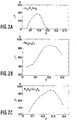
- the operation of the transistor 10 is optimal when the number p of charge carriers of the superconductive layer with zero electric field is adjusted so that the critical temperature T c is very sensitive to the variations in the number p which are induced when a electric field is applied in the channel.
- This adjustment made for example with reference to the curve shown in FIG. 2B relating to YBa2Cu3O7, must therefore be made on the steep end portion of the curve. The number p is thus brought into a part most favorable to the production of an important field effect.
- each superconductive layer 17 a thickness of the order of magnitude of the length of Debye L D , of the order of a few nanometers.
- the thickness of each non-superconductive layer is determined experimentally so as to obtain a concentration p of charge carriers for which the ratio dT c / dp is optimal. This can be done with reference to a curve of the type represented in FIG. 3.
- this reference curve illustrates the variation of the critical temperature T c in Kelvins which makes it possible to obtain, as a function of the thickness w of each non-superconductive layer 18, a predetermined percentage of the resistance in the normal state of each layer 18 when the superconductive layers 18 have a predetermined fixed thickness.
- the dielectric layer 18 also has a thickness of the order of the length of Debye L D.
- each of these two layers is made of at least one superimposed crystalline mesh, the number of these corresponding meshes being fixed so as to obtain the desired thickness of each of the layers.
- the layers of the channel structure 14 were formed by epitaxial growth to have the desired interface.
- the choice of materials in the paired layers of the structure must ensure their compatibility with epitaxial growth. This condition is satisfied with the association YBa2Cu3O7 / PrBa2Cu3O7 described above.
- the method can be applied to other materials than PrBa2Cu3O7 in the case where YBa2Cu3O7 is used, and to other superconductive materials than YBa2Cu3O7.
- the non-superconductive layers of the channel structure 14 may be dielectric layers like those mentioned above, or be semiconductor layers doped or not, or alternatively layers made of a metallic material.
- a transistor 10 according to the invention could operate with a single pair of layers 17, 18 in the channel structure 14.
- this structure could only pass a very low maximum current.
- This structure then allows the passage of a current of total intensity proportional to the number of pairs of layers under a low drain-source voltage and under the action of an equally low gate voltage.
- a channel structure 14 formed of three pairs of layers made in the manner described above can pass a current of a few mA with a drain-source voltage of the order of 10mV and under the action of a gate voltage. only a few volts.
- the multilayer structure of the channel 14 is electrically equivalent to the placing in series of electrical capacitors. It follows that the total input capacity of a transistor 10 according to the invention is low compared to a transistor whose channel would be reduced to a single superconductive layer 17. One of the advantages of this low capacity is increase the bandwidth of the transistor to very high frequencies.
- the high values of the electric field necessary to obtain the desired effect can be more easily obtained if the gate insulation film 16 has a high dielectric permittivity. This condition is therefore contrary to that relating to non-superconductive MOS transistors.
- the source and drain electrodes do not necessarily have to be superconductive. They can be made of a metallic material or of a doped semiconductor material. It is the same for the gate electrode 15. However, these materials do not offer the advantages of electrical conduction of HTSC materials.
Landscapes
- Chemical & Material Sciences (AREA)
- Engineering & Computer Science (AREA)
- Ceramic Engineering (AREA)
- Superconductor Devices And Manufacturing Methods Thereof (AREA)
- Inorganic Compounds Of Heavy Metals (AREA)
- Crystals, And After-Treatments Of Crystals (AREA)
- Thin Film Transistor (AREA)
Applications Claiming Priority (2)
| Application Number | Priority Date | Filing Date | Title |
|---|---|---|---|
| FR9103529 | 1991-03-22 | ||
| FR9103529A FR2674374A1 (fr) | 1991-03-22 | 1991-03-22 | Transistor supraconducteur a effet de champ et procede de fabrication d'une structure multicouche telle que celle utilisee dans le transistor. |
Publications (3)
| Publication Number | Publication Date |
|---|---|
| EP0505259A2 true EP0505259A2 (de) | 1992-09-23 |
| EP0505259A3 EP0505259A3 (en) | 1993-01-27 |
| EP0505259B1 EP0505259B1 (de) | 2000-02-23 |
Family
ID=9411041
Family Applications (1)
| Application Number | Title | Priority Date | Filing Date |
|---|---|---|---|
| EP92400697A Expired - Lifetime EP0505259B1 (de) | 1991-03-22 | 1992-03-16 | Supraleitender Feldeffekttransistor und Verfahren zur Herstellung einer Mehrfachlagenstruktur für diesen Transistor |
Country Status (5)
| Country | Link |
|---|---|
| EP (1) | EP0505259B1 (de) |
| JP (2) | JP2591559B2 (de) |
| DE (1) | DE69230698T2 (de) |
| ES (1) | ES2143986T3 (de) |
| FR (1) | FR2674374A1 (de) |
Cited By (7)
| Publication number | Priority date | Publication date | Assignee | Title |
|---|---|---|---|---|
| EP0533519A3 (en) * | 1991-08-26 | 1993-05-05 | Sumitomo Electric Industries, Ltd. | Superconducting device having an extremely thin superconducting channel formed of oxide superconductor material and method for manufacturing the same |
| EP0545801A1 (de) * | 1991-11-30 | 1993-06-09 | Sumitomo Electric Industries, Ltd. | Supraleitendes Bauelement mit extrem dünnen supraleitenden Kanal und Herstellungsverfahren |
| EP0546959A3 (en) * | 1991-12-13 | 1993-07-14 | Sumitomo Electric Industries, Ltd. | Superconducting device having an extremely thin superconducting channel formed of oxide superconductor material and method for manufacturing the same |
| US5506197A (en) * | 1991-12-13 | 1996-04-09 | Sumitomo Electric Industries, Ltd. | Superconducting device having an extremely thin superconducting channel formed of oxide superconductor material |
| EP0701292A3 (de) * | 1992-06-29 | 1997-03-26 | Matsushita Electric Industrial Co Ltd | Supraleitendes Bauelement des Feld-Effekt-Typs |
| FR2835353A1 (fr) * | 2002-01-25 | 2003-08-01 | Wintici | Dispositifs electroniques de commande a base de materiau supraconducteur |
| CN102664153A (zh) * | 2012-05-08 | 2012-09-12 | 肖德元 | 一种超导场效应晶体管、其制作方法及应用方法 |
Families Citing this family (1)
| Publication number | Priority date | Publication date | Assignee | Title |
|---|---|---|---|---|
| JPH0831625B2 (ja) * | 1992-10-30 | 1996-03-27 | 株式会社日立製作所 | 超電導三端子素子 |
Family Cites Families (4)
| Publication number | Priority date | Publication date | Assignee | Title |
|---|---|---|---|---|
| JPS63160273A (ja) * | 1986-12-23 | 1988-07-04 | Fujitsu Ltd | 高速半導体装置 |
| DE3876228T2 (de) * | 1988-01-15 | 1993-06-03 | Ibm | Feldeffektanordnung mit supraleitendem kanal. |
| JPH0260176A (ja) * | 1988-08-26 | 1990-02-28 | Japan Aviation Electron Ind Ltd | アハロノフ・ボーム効果トランジスタ |
| EP0494580B1 (de) * | 1991-01-07 | 2002-04-03 | International Business Machines Corporation | Supraleitender Feldeffekttransistor mit inverser MISFET-Struktur und Verfahren zu dessen Herstellung |
-
1991
- 1991-03-22 FR FR9103529A patent/FR2674374A1/fr active Granted
-
1992
- 1992-03-16 ES ES92400697T patent/ES2143986T3/es not_active Expired - Lifetime
- 1992-03-16 DE DE69230698T patent/DE69230698T2/de not_active Expired - Fee Related
- 1992-03-16 EP EP92400697A patent/EP0505259B1/de not_active Expired - Lifetime
- 1992-03-19 JP JP4063741A patent/JP2591559B2/ja not_active Expired - Lifetime
-
1995
- 1995-09-28 JP JP7251519A patent/JPH08191157A/ja active Pending
Cited By (13)
| Publication number | Priority date | Publication date | Assignee | Title |
|---|---|---|---|---|
| EP0533519A3 (en) * | 1991-08-26 | 1993-05-05 | Sumitomo Electric Industries, Ltd. | Superconducting device having an extremely thin superconducting channel formed of oxide superconductor material and method for manufacturing the same |
| US5494891A (en) * | 1991-11-30 | 1996-02-27 | Sumitomo Electric Industries, Ltd. | Method for manufacturing three-terminal oxide superconducting devices |
| EP0545801A1 (de) * | 1991-11-30 | 1993-06-09 | Sumitomo Electric Industries, Ltd. | Supraleitendes Bauelement mit extrem dünnen supraleitenden Kanal und Herstellungsverfahren |
| US5399546A (en) * | 1991-11-30 | 1995-03-21 | Sumitomo Electric Industries, Ltd. | Superconducting device having an extremely thin superconducting channel formed of oxide superconductor material |
| US5539215A (en) * | 1991-12-13 | 1996-07-23 | Sumitomo Electric Industries, Ltd. | Superconducting device having an extremely thin superconducting channel formed of oxide superconductor material |
| US5506197A (en) * | 1991-12-13 | 1996-04-09 | Sumitomo Electric Industries, Ltd. | Superconducting device having an extremely thin superconducting channel formed of oxide superconductor material |
| EP0546959A3 (en) * | 1991-12-13 | 1993-07-14 | Sumitomo Electric Industries, Ltd. | Superconducting device having an extremely thin superconducting channel formed of oxide superconductor material and method for manufacturing the same |
| US5789346A (en) * | 1991-12-13 | 1998-08-04 | Sumitomo Electric Industries, Ltd. | Method for manufacturing an oxide superconductor device |
| EP0701292A3 (de) * | 1992-06-29 | 1997-03-26 | Matsushita Electric Industrial Co Ltd | Supraleitendes Bauelement des Feld-Effekt-Typs |
| US5828079A (en) * | 1992-06-29 | 1998-10-27 | Matsushita Electric Industrial Co., Ltd. | Field-effect type superconducting device including bi-base oxide compound containing copper |
| FR2835353A1 (fr) * | 2002-01-25 | 2003-08-01 | Wintici | Dispositifs electroniques de commande a base de materiau supraconducteur |
| WO2003063259A3 (fr) * | 2002-01-25 | 2004-04-01 | Wintici | Dispositifs electroniques de commande a base de materiau supraconducteur |
| CN102664153A (zh) * | 2012-05-08 | 2012-09-12 | 肖德元 | 一种超导场效应晶体管、其制作方法及应用方法 |
Also Published As
| Publication number | Publication date |
|---|---|
| JP2591559B2 (ja) | 1997-03-19 |
| DE69230698D1 (de) | 2000-03-30 |
| JPH06237023A (ja) | 1994-08-23 |
| FR2674374A1 (fr) | 1992-09-25 |
| DE69230698T2 (de) | 2000-06-15 |
| FR2674374B1 (de) | 1997-02-07 |
| EP0505259A3 (en) | 1993-01-27 |
| EP0505259B1 (de) | 2000-02-23 |
| ES2143986T3 (es) | 2000-06-01 |
| JPH08191157A (ja) | 1996-07-23 |
Similar Documents
| Publication | Publication Date | Title |
|---|---|---|
| Mannhart et al. | Electric field effect on superconducting YBa2Cu3O7− δ films | |
| FR2626715A1 (fr) | Dispositif en couches minces de materiau supraconducteur et procede de realisation | |
| EP2294637A1 (de) | Feldeffekt-supraleitertransistor und verfahren zur herstellung eines solchen transistors | |
| EP0511056B1 (de) | Josephsonjunctionstruktur | |
| EP0494580B1 (de) | Supraleitender Feldeffekttransistor mit inverser MISFET-Struktur und Verfahren zu dessen Herstellung | |
| EP0505259B1 (de) | Supraleitender Feldeffekttransistor und Verfahren zur Herstellung einer Mehrfachlagenstruktur für diesen Transistor | |
| JPH03174781A (ja) | 放射線検出素子およびジョセフソン素子 | |
| JPH104223A (ja) | 酸化物超電導体ジョセフソン素子 | |
| EP0508843B1 (de) | Josephsoneffekt-Halbleiteranordnung | |
| Kroger | Josephson devices coupled by semiconductor links | |
| US5447907A (en) | Superconducting device with c-axis channel and a-axis source and drain having a continuous crystal structure | |
| EP0083621B1 (de) | Verfahren zum erhöhen der kritischen temperatur in quasi-eindimensionalen organischen supraleitern und nach diesem verfahren erhaltene neue supraleitende verbindungen | |
| Muramatsu et al. | Photocarrier Injection and Current–Voltage Characteristics of La0. 8Sr0. 2MnO3/SrTiO3: Nb Heterojunction at Low Temperature | |
| Uematsu et al. | Intrinsic Josephson effect in La 2− x Sr x CuO 4 mesa junctions with niobium counter electrode | |
| Morohashi et al. | High‐quality Nb/HfO x‐Hf/Nb Josephson junction | |
| Jiranapakul et al. | Photoelectric properties of oxygen-doped a-Si: H prepared by rf sputtering | |
| Nevala et al. | Fabrication and characterization of epitaxial NbN/TaN/NbN Josephson junctions grown by pulsed laser ablation | |
| JP2774713B2 (ja) | 超電導素子 | |
| FR2463512A1 (fr) | Perfectionnements aux dispositifs a jonctions tunnel et aux procedes de fabrication de telles jonctions | |
| Alexanian et al. | On resonance phototunneling and photoelectric properties ofpInSb-nCdTe heterojunction | |
| FR2545988A1 (fr) | Transistor a effet de champ, fonctionnant en mode de desertion profonde | |
| Suh et al. | Superconductivity and electric field effect of 90 degree grain boundaries in YBa2Cu/sub 3/O/sub 7-x/thin films | |
| JPH06164002A (ja) | 超電導光センサ | |
| WO2017198866A1 (fr) | Dispositif comprenant une jonction josephson | |
| Rahman et al. | Current switching in superconductor–semiconductor bilayers |
Legal Events
| Date | Code | Title | Description |
|---|---|---|---|
| PUAI | Public reference made under article 153(3) epc to a published international application that has entered the european phase |
Free format text: ORIGINAL CODE: 0009012 |
|
| AK | Designated contracting states |
Kind code of ref document: A2 Designated state(s): DE ES FR GB IT SE |
|
| PUAL | Search report despatched |
Free format text: ORIGINAL CODE: 0009013 |
|
| AK | Designated contracting states |
Kind code of ref document: A3 Designated state(s): DE ES FR GB IT SE |
|
| 17P | Request for examination filed |
Effective date: 19921218 |
|
| RAP3 | Party data changed (applicant data changed or rights of an application transferred) |
Owner name: BULL S.A. |
|
| 17Q | First examination report despatched |
Effective date: 19950816 |
|
| GRAG | Despatch of communication of intention to grant |
Free format text: ORIGINAL CODE: EPIDOS AGRA |
|
| GRAG | Despatch of communication of intention to grant |
Free format text: ORIGINAL CODE: EPIDOS AGRA |
|
| GRAH | Despatch of communication of intention to grant a patent |
Free format text: ORIGINAL CODE: EPIDOS IGRA |
|
| GRAH | Despatch of communication of intention to grant a patent |
Free format text: ORIGINAL CODE: EPIDOS IGRA |
|
| GRAA | (expected) grant |
Free format text: ORIGINAL CODE: 0009210 |
|
| AK | Designated contracting states |
Kind code of ref document: B1 Designated state(s): DE ES FR GB IT SE |
|
| GBT | Gb: translation of ep patent filed (gb section 77(6)(a)/1977) |
Effective date: 20000223 |
|
| REF | Corresponds to: |
Ref document number: 69230698 Country of ref document: DE Date of ref document: 20000330 |
|
| ITF | It: translation for a ep patent filed | ||
| REG | Reference to a national code |
Ref country code: ES Ref legal event code: FG2A Ref document number: 2143986 Country of ref document: ES Kind code of ref document: T3 |
|
| EN | Fr: translation not filed | ||
| EN4 | Fr: notification of non filing translation in an earlier bopi is erroneous | ||
| PLBE | No opposition filed within time limit |
Free format text: ORIGINAL CODE: 0009261 |
|
| STAA | Information on the status of an ep patent application or granted ep patent |
Free format text: STATUS: NO OPPOSITION FILED WITHIN TIME LIMIT |
|
| 26N | No opposition filed | ||
| REG | Reference to a national code |
Ref country code: GB Ref legal event code: IF02 |
|
| PGFP | Annual fee paid to national office [announced via postgrant information from national office to epo] |
Ref country code: SE Payment date: 20060222 Year of fee payment: 15 |
|
| PGFP | Annual fee paid to national office [announced via postgrant information from national office to epo] |
Ref country code: GB Payment date: 20060223 Year of fee payment: 15 |
|
| PGFP | Annual fee paid to national office [announced via postgrant information from national office to epo] |
Ref country code: DE Payment date: 20060227 Year of fee payment: 15 |
|
| PGFP | Annual fee paid to national office [announced via postgrant information from national office to epo] |
Ref country code: ES Payment date: 20060309 Year of fee payment: 15 |
|
| PG25 | Lapsed in a contracting state [announced via postgrant information from national office to epo] |
Ref country code: SE Free format text: LAPSE BECAUSE OF NON-PAYMENT OF DUE FEES Effective date: 20070317 |
|
| EUG | Se: european patent has lapsed | ||
| GBPC | Gb: european patent ceased through non-payment of renewal fee |
Effective date: 20070316 |
|
| PGFP | Annual fee paid to national office [announced via postgrant information from national office to epo] |
Ref country code: IT Payment date: 20070619 Year of fee payment: 16 |
|
| PG25 | Lapsed in a contracting state [announced via postgrant information from national office to epo] |
Ref country code: DE Free format text: LAPSE BECAUSE OF NON-PAYMENT OF DUE FEES Effective date: 20071002 |
|
| PG25 | Lapsed in a contracting state [announced via postgrant information from national office to epo] |
Ref country code: GB Free format text: LAPSE BECAUSE OF NON-PAYMENT OF DUE FEES Effective date: 20070316 |
|
| REG | Reference to a national code |
Ref country code: ES Ref legal event code: FD2A Effective date: 20070317 |
|
| PG25 | Lapsed in a contracting state [announced via postgrant information from national office to epo] |
Ref country code: ES Free format text: LAPSE BECAUSE OF NON-PAYMENT OF DUE FEES Effective date: 20070317 |
|
| PG25 | Lapsed in a contracting state [announced via postgrant information from national office to epo] |
Ref country code: IT Free format text: LAPSE BECAUSE OF NON-PAYMENT OF DUE FEES Effective date: 20080316 |
|
| PGFP | Annual fee paid to national office [announced via postgrant information from national office to epo] |
Ref country code: FR Payment date: 20110412 Year of fee payment: 20 |