EP0505259A2 - Superconducting field effect transistor and method for making a multilayer structure used in that transistor - Google Patents
Superconducting field effect transistor and method for making a multilayer structure used in that transistor Download PDFInfo
- Publication number
- EP0505259A2 EP0505259A2 EP19920400697 EP92400697A EP0505259A2 EP 0505259 A2 EP0505259 A2 EP 0505259A2 EP 19920400697 EP19920400697 EP 19920400697 EP 92400697 A EP92400697 A EP 92400697A EP 0505259 A2 EP0505259 A2 EP 0505259A2
- Authority
- EP
- European Patent Office
- Prior art keywords
- superconductive
- layer
- thickness
- layers
- superconductive layer
- Prior art date
- Legal status (The legal status is an assumption and is not a legal conclusion. Google has not performed a legal analysis and makes no representation as to the accuracy of the status listed.)
- Granted
Links
Images
Classifications
-
- H—ELECTRICITY
- H10—SEMICONDUCTOR DEVICES; ELECTRIC SOLID-STATE DEVICES NOT OTHERWISE PROVIDED FOR
- H10N—ELECTRIC SOLID-STATE DEVICES NOT OTHERWISE PROVIDED FOR
- H10N60/00—Superconducting devices
- H10N60/80—Constructional details
- H10N60/85—Superconducting active materials
- H10N60/855—Ceramic superconductors
- H10N60/857—Ceramic superconductors comprising copper oxide
- H10N60/858—Ceramic superconductors comprising copper oxide having multilayered structures, e.g. superlattices
-
- H—ELECTRICITY
- H10—SEMICONDUCTOR DEVICES; ELECTRIC SOLID-STATE DEVICES NOT OTHERWISE PROVIDED FOR
- H10N—ELECTRIC SOLID-STATE DEVICES NOT OTHERWISE PROVIDED FOR
- H10N60/00—Superconducting devices
- H10N60/20—Permanent superconducting devices
- H10N60/205—Permanent superconducting devices having three or more electrodes, e.g. transistor-like structures
- H10N60/207—Field effect devices
Definitions
- the invention relates to a superconductive field effect transistor and to a method of manufacturing a multilayer structure such as that used in the transistor.
- HTSC High Temperature Super-Conductor
- oxide critical high temperature superconducting material
- FET superconductive field effect transistor
- the superconductive transistor is similar to a conventional field effect transistor and comprises, on the surface of a semiconductor substrate of InSb, InAs or InAsGa for example, an epitaxial semiconductor layer doped with n conductivity type serving as a support for source and drain superconductive electrodes delimiting in the epitaxial layer a channel covered by a gate insulation layer supporting the gate electrode.
- the source-drain distance which defines the electrical length of the transistor channel, corresponds substantially to the coherence length of the superconducting material so as to allow diffusion of Cooper pairs between the source and the drain by Josephson effect.
- the maximum superconductive current I o which can pass through a Josephson junction is inversely proportional to the resistance R n in the normal state of the barrier of the junction.
- the canal plays the role of this barrier.
- the channel epitaxial layer allows the proximity effect of the superconducting charge carriers to pass.
- the device therefore has a transistor effect.
- the second operating principle of a superconductive field effect transistor is illustrated for example in the Japanese patent application published under the number 01-155671.
- the transistor described therein is formed from a metal substrate.
- One face of the substrate carries a multilayer structure made of a dielectric layer covered with a superconductive layer defining a channel between the source and drain electrodes.
- the other side of the substrate carries a control electrode.
- the dielectric layer given as an example was made of oriented SrTiO3 (100) and 200 nm thick, or thick MgO of 150 nm.
- the superconductive layer belonged to the RE-Ba-Cu-O family and was 60 nm thick. In operation, the number of charge carriers which pass through the superconducting channel is adjusted by the electric field produced by the control voltage.
- This electric field causes an accumulation of charges at the interface of the superconductive layer with the dielectric layer and destroys electronic pairs in the superconductive layer. This destruction removes the superconductivity of the superconductive layer and therefore reduces the current flowing through it.
- the inventors claim to have observed such an effect in a transistor including a superconductive layer of YBa2Cu3O 6 + x separated, via a dielectric layer SrTiO3 thick of 200 nm, from a control electrode brought to a voltage of 450 V .
- the control voltage to be applied to the substrate of the transistor to obtain the desired field effect is very high (450 volts, in the example cited), incompatible with current applications of the transistors.
- the Japanese document reports the observation of a current between the source and the drain, without indicating the value. In reality, this current has a very low intensity.
- the superconductive layer carrying this current had a relatively high thickness (60 nm), as did the thickness of the underlying dielectric layer (150 or 200 nm depending on the material used). A decrease in the thickness of the superconductive layer suggests a decrease in the current, while experience shows that an increase in the thickness does not produce a significantly greater current.
- the aforementioned Japanese document gives no indication of the parameters determining the variation in the value of the field effect produced by the prior transistor. It therefore does not optimize the field effect.
- those skilled in the art could think of adjusting the number p of charge carriers in HTSC material.
- the concentration of charge carriers can in fact be adjusted by acting on the oxygen concentration in the HTSC material.
- the oxygen concentration is difficult to control.
- the invention remedies these drawbacks and presents a superconductive field effect transistor capable of conducting large currents, of a few mA for example, under a low drain-source voltage of the order of 10 mV for example, and under the control low voltage, only a few volts.
- the invention further presents a method for adjusting the number p of free carriers for optimizing the field effect.
- a field effect superconductive transistor comprising a substrate carrying a structure made of a non-superconductive layer covered with a superconductive layer defining a channel between source and drain electrodes, and a gate electrode, is characterized in that the gate electrode is arranged on the channel and the superconductive layer has a thickness of the order of magnitude of the Debye length, the structure being able to be repeated n times and being made so that the layers have continuous interfaces between them.
- the invention also relates to a method for manufacturing a multilayer structure such as that defined above, comprising at least one pair made of a non-superconductive layer covered with a superconductive layer, characterized in that it consists in adjusting the thickness of the layers of each pair so that the critical temperature T c varies greatly as a function of the number (p) of charge carriers in the superconductive layer in zero electric field and that the thickness of the non-superconductive layer allows reception optimal charge carriers provided by the superconductive layer.
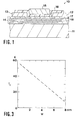
- the field effect superconductive transistor 10 has an insulated gate structure, for example of the MOS (Metal-Oxide-Semiconductor) type. It is formed on the surface of a substrate 11 and comprises a source electrode 12 and a drain electrode 13 resting on a structure constituting a current channel 14 between these two electrodes.
- the channel 14 carries a gate electrode 15 via a gate insulation film 16.
- the dimension ratios shown in Figure 1 have been intentionally modified for clarity of drawings.
- the transistor 10 has the substrate made of MgO, the source and drain electrodes 12, 13 and the grid 15 made of YBa2Cu3O7 superconductive material and the grid insulation film 16 in SiO2.
- the channel 14 is formed of a multilayer structure resting on the substrate 11.
- the channel structure 14 is made from a superconductive layer 17 and a non-superconductive layer 18.
- the pair of layers 17 and 18 is repeated three times in the channel structure 14. In each pair, the superconductive layer 17 is the upper layer.
- each superconductive layer 17 has a very small thickness, of the order of only a few nanometers. The inventors have attempted to explain this value by the following theory, which gives this thickness the order of magnitude of the Debye length L D.
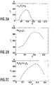
- the critical temperature T c goes from 80K to 70K when the number p decreases from 0.16 to 0.13 charge carriers per group of Cu-O.
- the transition between the superconducting state and the normal state, caused by the application of an electric field, is due to the fact that the critical temperature T c of the zone depleted in carriers of load becomes lower than its zero field operating temperature. Under these conditions, the depth of penetration of the electric field into the channel could be roughly assessed in the following manner.
- the channel structure 14 of the transistor shown in FIG. 1 has been based on the article by JM Triscone et al in the journal Physical Review Letters, Vol. 64, No 7, Feb. 12, 1990, pages 804-807, entitled "YBa2Cu3O7 / PrBa2Cu3O7 Superlattices: Properties of Ultrathin Superconducting Layers Separated by Insulating Layers".
- the structure described is formed by a non-zero whole number of superimposed pairs, each composed of an upper superconductive layer 17 of YBa2Cu3O7 and a dielectric layer 18 of YBa2Cu3O7.
- the superconductive layer 17 of each pair had a thickness of a few nanometers, corresponding approximately to the length of Debye L D.
- the transistor 10 provided with this multilayer channel structure 14 in the transistor 10 makes it possible to pass a larger source-drain current with a low control voltage.
- the method consists in optimizing the charge transfers between the layers of each pair.
- the operation of the transistor 10 is optimal when the number p of charge carriers of the superconductive layer with zero electric field is adjusted so that the critical temperature T c is very sensitive to the variations in the number p which are induced when a electric field is applied in the channel.
- This adjustment made for example with reference to the curve shown in FIG. 2B relating to YBa2Cu3O7, must therefore be made on the steep end portion of the curve. The number p is thus brought into a part most favorable to the production of an important field effect.
- each superconductive layer 17 a thickness of the order of magnitude of the length of Debye L D , of the order of a few nanometers.
- the thickness of each non-superconductive layer is determined experimentally so as to obtain a concentration p of charge carriers for which the ratio dT c / dp is optimal. This can be done with reference to a curve of the type represented in FIG. 3.
- this reference curve illustrates the variation of the critical temperature T c in Kelvins which makes it possible to obtain, as a function of the thickness w of each non-superconductive layer 18, a predetermined percentage of the resistance in the normal state of each layer 18 when the superconductive layers 18 have a predetermined fixed thickness.
- the dielectric layer 18 also has a thickness of the order of the length of Debye L D.
- each of these two layers is made of at least one superimposed crystalline mesh, the number of these corresponding meshes being fixed so as to obtain the desired thickness of each of the layers.
- the layers of the channel structure 14 were formed by epitaxial growth to have the desired interface.
- the choice of materials in the paired layers of the structure must ensure their compatibility with epitaxial growth. This condition is satisfied with the association YBa2Cu3O7 / PrBa2Cu3O7 described above.
- the method can be applied to other materials than PrBa2Cu3O7 in the case where YBa2Cu3O7 is used, and to other superconductive materials than YBa2Cu3O7.
- the non-superconductive layers of the channel structure 14 may be dielectric layers like those mentioned above, or be semiconductor layers doped or not, or alternatively layers made of a metallic material.
- a transistor 10 according to the invention could operate with a single pair of layers 17, 18 in the channel structure 14.
- this structure could only pass a very low maximum current.
- This structure then allows the passage of a current of total intensity proportional to the number of pairs of layers under a low drain-source voltage and under the action of an equally low gate voltage.
- a channel structure 14 formed of three pairs of layers made in the manner described above can pass a current of a few mA with a drain-source voltage of the order of 10mV and under the action of a gate voltage. only a few volts.
- the multilayer structure of the channel 14 is electrically equivalent to the placing in series of electrical capacitors. It follows that the total input capacity of a transistor 10 according to the invention is low compared to a transistor whose channel would be reduced to a single superconductive layer 17. One of the advantages of this low capacity is increase the bandwidth of the transistor to very high frequencies.
- the high values of the electric field necessary to obtain the desired effect can be more easily obtained if the gate insulation film 16 has a high dielectric permittivity. This condition is therefore contrary to that relating to non-superconductive MOS transistors.
- the source and drain electrodes do not necessarily have to be superconductive. They can be made of a metallic material or of a doped semiconductor material. It is the same for the gate electrode 15. However, these materials do not offer the advantages of electrical conduction of HTSC materials.
Landscapes
- Chemical & Material Sciences (AREA)
- Engineering & Computer Science (AREA)
- Ceramic Engineering (AREA)
- Superconductor Devices And Manufacturing Methods Thereof (AREA)
- Inorganic Compounds Of Heavy Metals (AREA)
- Crystals, And After-Treatments Of Crystals (AREA)
- Thin Film Transistor (AREA)
Abstract
Description
L'invention se rapporte à un transistor supraconducteur à effet de champ et à un procédé de fabrication d'une structure multicouche telle que celle utilisée dans le transistor.The invention relates to a superconductive field effect transistor and to a method of manufacturing a multilayer structure such as that used in the transistor.
On appelle ordinairement dans ce domaine un matériau HTSC (High Temperature Super-Conductor) un matériau supraconducteur à haute température critique, couramment un oxyde. Depuis l'apparition des oxydes HTSC en 1986, des travaux ont été menés pour étudier leur emploi éventuel dans le domaine de l'électronique. La supraconductivité ouvrait en effet la perspective de réaliser des dispositifs rapides à très faible consommation d'énergie et fonctionnant à la température de l'azote liquide. Différents transistors supraconducteurs à effet de champ ont déjà été présentés. On distingue actuellement deux principes de fonctionnement des transistors à effet de champ (FET) supraconducteurs.In this field, an HTSC (High Temperature Super-Conductor) material is usually called a critical high temperature superconducting material, commonly an oxide. Since the appearance of HTSC oxides in 1986, work has been carried out to study their possible use in the field of electronics. Superconductivity opened up the prospect of making rapid devices with very low energy consumption and operating at the temperature of liquid nitrogen. Various superconductive field effect transistors have already been presented. There are currently two operating principles for superconductive field effect transistors (FETs).
Le premier principe a été proposé pour la première fois par T.D. Clark dans sa thèse soutenue à l'université de Londres en 1971 (non publiée). Le transistor supraconducteur est semblable à un transistor à effet de champ classique et comprend, à la surface d'un substrat semiconducteur de InSb, de InAs ou de InAsGa par exemple, une couche semiconductrice épitaxiale dopée de type de conductivite n servant de support à des électrodes supraconductrices de source et de drain délimitant dans la couche épitaxiale un canal recouvert par une couche d'isolation de grille supportant l'électrode de grille. La distance source-drain, qui définit la longueur électrique du canal du transistor, correspond sensiblement à la longueur de cohérence du matériau supraconducteur de façon à permettre la diffusion de paires de Cooper entre la source et le drain par effet Josephson. Il est connu que le courant supraconducteur maximal Io pouvant traverser une jonction Josephson est inversement proportionnel à la résistance Rn à l'état normal de la barrière de la jonction. Le canal joue le rôle de cette barrière. La couche épitaxiale de canal laisse passer par effet de proximité des porteurs de charge supraconducteurs. La nature semiconductrice du canal permet, en appliquant une tension de commande sur la grille, de moduler le nombre de porteurs de charge présents et de faire varier en conséquence la valeur de la résistance Rn. Si un courant I constant et supérieur à Io circule entre la source et le drain, la tension VDS entre ces deux électrodes satisfait à la relation VDS = Rn(I²- Io²)1/2. Le dispositif présente donc bien un effet transistor. Sa construction est bien adaptée aux matériaux supraconducteurs classiques à basse température tels que les composés au niobium, car leur longueur de cohérence est en général relativement grande (de l'ordre de 100nm). Les matériaux HTSC présentent par contre une longueur de cohérence beaucoup plus faible (de l'ordre de quelques nanomètres), qui rend alors la réalisation du transistor très difficile.The first principle was first proposed by TD Clark in his thesis defended at the University of London in 1971 (unpublished). The superconductive transistor is similar to a conventional field effect transistor and comprises, on the surface of a semiconductor substrate of InSb, InAs or InAsGa for example, an epitaxial semiconductor layer doped with n conductivity type serving as a support for source and drain superconductive electrodes delimiting in the epitaxial layer a channel covered by a gate insulation layer supporting the gate electrode. The source-drain distance, which defines the electrical length of the transistor channel, corresponds substantially to the coherence length of the superconducting material so as to allow diffusion of Cooper pairs between the source and the drain by Josephson effect. It is known that the maximum superconductive current I o which can pass through a Josephson junction is inversely proportional to the resistance R n in the normal state of the barrier of the junction. The canal plays the role of this barrier. The channel epitaxial layer allows the proximity effect of the superconducting charge carriers to pass. The semiconductor nature of the channel makes it possible, by applying a control voltage to the gate, to modulate the number of charge carriers present and to vary the value of the resistance R n accordingly . If a current I constant and greater than I o flows between the source and the drain, the voltage VDS between these two electrodes satisfies the relation V DS = R n (I²- I o ²) 1/2 . The device therefore has a transistor effect. Its construction is well suited to conventional superconducting materials at low temperature such as niobium compounds, because their coherence length is generally relatively large (of the order of 100nm). HTSC materials, on the other hand, have a much shorter coherence length (of the order of a few nanometers), which then makes it very difficult to make the transistor.
Le deuxième principe de fonctionnement d'un transistor supraconducteur à effet de champ est illustré par exemple dans la demande de brevet japonais publiée sous le n° 01-155671. Le transistor qui y est décrit est formé à partir d'un substrat métallique. Une face du substrat porte une structure multicouche faite d'une couche diélectrique recouverte d'une couche supraconductrice définissant un canal entre les électrodes de source et de drain. L'autre face du substrat porte une électrode de commande. La couche diélectrique donnée à titre d'exemple était faite de SrTiO₃ orienté (100) et épaisse de 200 nm, ou de MgO épais de 150 nm. La couche supraconductrice appartenait à la famille RE-Ba-Cu-O et était épaisse de 60 nm. En fonctionnement, le nombre des porteurs de charge qui transitent dans le canal supraconducteur est ajusté par le champ électrique produit par la tension de commande. Ce champ électrique provoque une accumulation de charges à l'interface de la couche supraconductrice avec la couche diélectrique et détruit des paires électroniques dans la couche supraconductrice. Cette destruction supprime la supraconductivité de la couche supraconductrice et réduit donc le courant qui la traverse. Les inventeurs assurent avoir observé un tel effet dans un transistor incluant une couche supraconductrice de YBa₂Cu₃O6+x séparée, par l'intermédiaire d'une couche diélectrique SrTiO₃ épaisse de 200 nm, d'une électrode de commande portée à une tension de 450 V.The second operating principle of a superconductive field effect transistor is illustrated for example in the Japanese patent application published under the number 01-155671. The transistor described therein is formed from a metal substrate. One face of the substrate carries a multilayer structure made of a dielectric layer covered with a superconductive layer defining a channel between the source and drain electrodes. The other side of the substrate carries a control electrode. The dielectric layer given as an example was made of oriented SrTiO₃ (100) and 200 nm thick, or thick MgO of 150 nm. The superconductive layer belonged to the RE-Ba-Cu-O family and was 60 nm thick. In operation, the number of charge carriers which pass through the superconducting channel is adjusted by the electric field produced by the control voltage. This electric field causes an accumulation of charges at the interface of the superconductive layer with the dielectric layer and destroys electronic pairs in the superconductive layer. This destruction removes the superconductivity of the superconductive layer and therefore reduces the current flowing through it. The inventors claim to have observed such an effect in a transistor including a superconductive layer of YBa₂Cu₃O 6 + x separated, via a dielectric layer SrTiO₃ thick of 200 nm, from a control electrode brought to a voltage of 450 V .
Ce principe de fonctionnement est intéressant, mais le transistor proposé présente trois inconvénients majeurs. D'abord, la tension de commande à appliquer sur le substrat du transistor pour obtenir l'effet de champ désiré est très élevée (450 volts, dans l'exemple cité), incompatible avec les applications courantes des transistors. Ensuite, le document japonais signale l'observation d'un courant entre la source et le drain, sans en indiquer la valeur. En réalité, ce courant a une très faible intensité. Pourtant, la couche supraconductrice véhiculant ce courant avait une épaisseur relativement élevée (60 nm), de même que l'épaisseur de la couche diélectrique sous-jacente (150 ou 200 nm selon le matériau utilisé). Une diminution de l'épaisseur de la couche supraconductrice laisse prévoir une diminution du courant, tandis que l'expérience révèle qu'une augmentation de l'épaisseur ne produit pas un courant sensiblement plus important. Enfin, le document japonais précité ne donne aucune indication sur les paramètres déterminant la variation de la valeur de l'effet de champ produit par le transistor antérieur. Il ne permet donc pas d'optimiser l'effet de champ. Afin d'accroître l'effet de champ du transistor antérieur, l'homme du métier pourrait penser à ajuster le nombre p de porteurs de charge dans le matériau HTSC. La concentration en porteurs de charge peut en effet être réglée en agissant sur la concentration en oxygène dans le matériau HTSC. Cependant, la concentration en oxygène est difficile à maîtriser.This operating principle is interesting, but the proposed transistor has three major drawbacks. First, the control voltage to be applied to the substrate of the transistor to obtain the desired field effect is very high (450 volts, in the example cited), incompatible with current applications of the transistors. Then, the Japanese document reports the observation of a current between the source and the drain, without indicating the value. In reality, this current has a very low intensity. However, the superconductive layer carrying this current had a relatively high thickness (60 nm), as did the thickness of the underlying dielectric layer (150 or 200 nm depending on the material used). A decrease in the thickness of the superconductive layer suggests a decrease in the current, while experience shows that an increase in the thickness does not produce a significantly greater current. Finally, the aforementioned Japanese document gives no indication of the parameters determining the variation in the value of the field effect produced by the prior transistor. It therefore does not optimize the field effect. In order to increase the field effect of the anterior transistor, those skilled in the art could think of adjusting the number p of charge carriers in HTSC material. The concentration of charge carriers can in fact be adjusted by acting on the oxygen concentration in the HTSC material. However, the oxygen concentration is difficult to control.
L'invention remédie à ces inconvénients et présente un transistor supraconducteur à effet de champ capable de conduire des courants importants, de quelques mA par exemple, sous une faible tension drain-source de l'ordre de 10 mV par exemple, et sous la commande d'une tension faible, de quelques volts seulement. L'invention présente en outre un procédé d'ajustement du nombre p de porteurs libres pour l'optimisation de l'effet de champ.The invention remedies these drawbacks and presents a superconductive field effect transistor capable of conducting large currents, of a few mA for example, under a low drain-source voltage of the order of 10 mV for example, and under the control low voltage, only a few volts. The invention further presents a method for adjusting the number p of free carriers for optimizing the field effect.
Un transistor supraconducteur à effet de champ conforme à l'invention, comprenant un substrat portant une structure faite d'une couche non supraconductrice recouverte d'une couche supraconductrice définissant un canal entre des électrodes de source et de drain, et une électrode de grille, est caractérisé en ce que l'électrode de grille est disposée sur le canal et la couche supraconductrice a une épaisseur de l'ordre de grandeur de la longueur de Debye, la structure pouvant se répéter n fois et étant faite de façon que les couches présentent des interfaces continues entre elles.A field effect superconductive transistor according to the invention, comprising a substrate carrying a structure made of a non-superconductive layer covered with a superconductive layer defining a channel between source and drain electrodes, and a gate electrode, is characterized in that the gate electrode is arranged on the channel and the superconductive layer has a thickness of the order of magnitude of the Debye length, the structure being able to be repeated n times and being made so that the layers have continuous interfaces between them.
L'invention se rapporte aussi à un procédé de fabrication d'une structure multicouche telle que celle définie précédemment, comprenant au moins une paire faite d'une couche non supraconductrice recouverte d'une couche supraconductrice, caractérisé en ce qu'il consiste à ajuster l'épaisseur des couches de chaque paire de façon que la température critique Tc varie fortement en fonction du nombre (p) de porteurs de charge dans la couche supraconductrice en champ électrique nul et que l'épaisseur de la couche non supraconductrice permette la réception optimale des porteurs de charge fournis par la couche supraconductrice.The invention also relates to a method for manufacturing a multilayer structure such as that defined above, comprising at least one pair made of a non-superconductive layer covered with a superconductive layer, characterized in that it consists in adjusting the thickness of the layers of each pair so that the critical temperature T c varies greatly as a function of the number (p) of charge carriers in the superconductive layer in zero electric field and that the thickness of the non-superconductive layer allows reception optimal charge carriers provided by the superconductive layer.
Les caractéristiques et avantages de l'invention ressortent de la description qui suit, donnée à titre d'exemple et faite en référence aux dessins annexés.The characteristics and advantages of the invention appear from the following description, given by way of example and made with reference to the accompanying drawings.
Dans les dessins :
- la figure 1 illustre schématiquement la structure vue en coupe transversale partielle d'un substrat portant un transistor supraconducteur à effet de champ conforme à l'invention ;
- les figures 2A, 2B et 2C sont des graphes illustrant les variations de la température critique Tc en kelvins avec le nombre p de porteurs de charge libres positifs par atome de cuivre dans respectivement les composés La2-xSrxCuO₄ , YBa₂Cu₃O₇ et Bi₂Sr₂CaCu₂Ox ; et
- la figure 3 est un graphe illustrant la variation de la température critique Tc en kelvins pour laquelle a été obtenu 10% de la résistance à l'état normal d'un ensemble de couches alternées de YBa₂Cu₃O₇ d'épaisseur constante de 1,2 nm et de PrBa₂Cu₃O₇ ayant chacune l'épaisseur w indiquée en abscisses.
- Figure 1 schematically illustrates the structure seen in partial cross section of a substrate carrying a field effect superconducting transistor according to the invention;
- FIGS. 2A, 2B and 2C are graphs illustrating the variations of the critical temperature T c in kelvins with the number p of positive free charge carriers per copper atom in the compounds La 2-x Sr x CuO₄, YBa₂Cu₃O₇ and Bi₂Sr₂CaCu₂O respectively x ; and
- FIG. 3 is a graph illustrating the variation of the critical temperature T c in kelvins for which 10% of the resistance in the normal state has been obtained from a set of alternating layers of YBa₂Cu₃O₇ of constant thickness of 1.2 nm and of PrBa₂Cu₃O₇ each having the thickness w indicated on the abscissa.
Le transistor supraconducteur à effet de champ 10 conforme à l'invention, représenté sur la figure 1, a une structure à grille isolée, par exemple de type MOS (Métal-Oxyde-Semiconducteur). Il est formé sur la surface d'un substrat 11 et comprend une électrode de source 12 et une électrode de drain 13 reposant sur une structure constituant un canal de courant 14 entre ces deux électrodes. Le canal 14 porte une électrode de grille 15 par l'intermédiaire d'un film d'isolation de grille 16. Les rapports des dimensions représentées sur la figure 1 ont été volontairement modifiés pour la clarté des dessins. Dans l'exemple préferé qui est illustré dans la figure 1, le transistor 10 a le substrat fait de MgO, les électrodes de source et de drain 12, 13 et la grille 15 en matériau supraconducteur YBa₂Cu₃O₇ et le film d'isolation de grille 16 en SiO₂. Le canal 14 est formé d'une structure multicouche reposant sur le substrat 11. La structure de canal 14 est faite à partir d'une couche supraconductrice 17 et d'une couche non supraconductrice 18. Dans l'exemple préféré qui est illustré dans la figure 1, la paire de couches 17 et 18 est répétée trois fois dans la structure de canal 14. Dans chaque paire, la couche supraconductrice 17 est la couche supérieure.The field effect
Dans la structure de canal 14, chaque couche supraconductrice 17 a une épaisseur très faible, de l'ordre de quelques nanomètres seulement. Les inventeurs ont tenté d'expliquer cette valeur par la théorie suivante, qui donne à cette épaisseur l'ordre de grandeur de la longueur de Debye LD.In the
Les nouveaux oxydes supraconducteurs doivent leur supraconductivité à l'existence dans leur maille élémentaire de plans incluant des atomes Cu et O. Les figures 2A, 2B et 2C annexées se rapportent respectivement aux oxydes supraconducteurs La2-xSrxCuO₄, YBa₂Cu₃O₇ et Bi₂Sr₂CaCu₂O₈ et font ressortir que la température critique Tc dépend très fortement du nombre p de porteurs de charge libres positifs par atome de cuivre dans les composés respectifs et, par conséquent, de la charge des groupes Cu-O des plans de leur maille. Par exemple, dans le cas de YBa₂Cu₃O₇ (figure 2B), la température critique Tc passe de 80K à 70K quand le nombre p décroît de 0,16 à 0,13 porteurs de charge par groupe de Cu-O. La transition entre l'état supraconducteur et l'état normal, provoquée par l'application d'un champ électrique, est due au fait que la température critique Tc de la zone appauvrie en porteurs de charge devient inférieure à sa température de fonctionnement à champ nul. Dans ces conditions, la profondeur de pénétration du champ électrique dans le canal pourrait s'apprécier grossièrement de la manière suivante. En assimilant les propriétés du matériau HTSC d'une couche supraconductrice à celles d'un matériau de type métallique, la profondeur de pénétration z d'un champ électrique E dans un tel matériau suit une loi exponentielle décroissante exprimée par la formule E = A e-z/LD , où A est un coefficient de proportionnalité et LD la longueur de Debye. La longueur de Debye LD dans un modèle simple de Thomas-Fermi vérifie la formule : LD = noe²/EEo, où no est la densité d'états au niveau de Fermi, e est la charge électronique, et Eo et E sont les permittivités respectives du vide et du matériau HTSC utilisé. Dans le cas de YBa₂Cu₃O₇, si le matériau HTSC est légèrement déficitaire en oxygène, on peut avoir environ no = 5.10²⁰ cm⁻³.eV⁻¹ et LD = 2,5 nm. Par conséquent, selon cette théorie, la densité de porteurs de charge ne peut varier que sur une profondeur maximale de quelques nanomètres. Cette théorie peut donc justifier en première approximation l'emploi d'une faible épaisseur de matériau HTSC dans le canal du transistor conforme à l'invention. D'après cette théorie, l'épaisseur serait de l'ordre de grandeur de la longueur de Debye, et si le matériau HTSC est plus épais, la partie du canal non soumise au champ électrique restera supraconductrice et masquera l'effet recherché.The new superconductive oxides owe their superconductivity to the existence in their elementary lattice of planes including atoms Cu and O. Figures 2A, 2B and 2C appended relate respectively to the superconductive oxides La 2-x Sr x CuO₄, YBa₂Cu₃O₇ and Bi₂Sr₂CaCu₂O₈ and show that the critical temperature T c very strongly depends on the number p of positive free charge carriers per atom of copper in the respective compounds and, consequently, on the charge of the Cu-O groups of the planes of their lattice. For example, in the case of YBa₂Cu₃O₇ (Figure 2B), the critical temperature T c goes from 80K to 70K when the number p decreases from 0.16 to 0.13 charge carriers per group of Cu-O. The transition between the superconducting state and the normal state, caused by the application of an electric field, is due to the fact that the critical temperature T c of the zone depleted in carriers of load becomes lower than its zero field operating temperature. Under these conditions, the depth of penetration of the electric field into the channel could be roughly assessed in the following manner. By assimilating the properties of the HTSC material of a superconductive layer to those of a metallic type material, the penetration depth z of an electric field E in such a material follows a decreasing exponential law expressed by the formula E = A e -z / LD , where A is a proportionality coefficient and L D the Debye length. The Debye length L D in a simple Thomas-Fermi model satisfies the formula: L D = n o e² / EE o , where n o is the density of states at Fermi level, e is the electronic charge, and E o and E are the respective permittivities of the vacuum and the HTSC material used. In the case of YBa₂Cu₃O₇, if the HTSC material is slightly deficient in oxygen, one can have approximately n o = 5.10²⁰ cm⁻³.eV⁻¹ and L D = 2.5 nm. Consequently, according to this theory, the density of charge carriers can only vary over a maximum depth of a few nanometers. This theory can therefore justify, as a first approximation, the use of a small thickness of HTSC material in the channel of the transistor according to the invention. According to this theory, the thickness would be of the order of magnitude of the length of Debye, and if the HTSC material is thicker, the part of the channel not subjected to the electric field will remain superconductive and will mask the desired effect.
L'avantage constaté est effectivement dans l'application d'une faible valeur de la tension de commande. Mais l'inconvénient demeure de n'obtenir qu'un très faible courant avec l'emploi d'une structure de canal 14 ayant une seule paire de couches 17, 18, dont la couche supraconductrice 17 a la faible épaisseur précitée.The advantage observed is actually in the application of a low value of the control voltage. However, the drawback remains of obtaining only a very low current with the use of a
Pour accroître l'intensité du courant, la structure de canal 14 du transistor représenté sur la figure 1 a été réalisée en s'inspirant de l'article de J.M. Triscone et al dans la revue Physical Review Letters, Vol. 64, No 7, Feb. 12, 1990, pages 804-807, intitulé « YBa₂Cu₃O₇/PrBa₂Cu₃O₇ Superlattices : Properties of Ultrathin Superconducting Layers Separated by Insulating Layers ». La structure décrite est formée d'un nombre entier non nul de paires superposées, composées chacune d'une couche supraconductrice supérieure 17 de YBa₂Cu₃O₇ et d'une couche diélectrique 18 de YBa₂Cu₃O₇. Conformément à l'invention, la couche supraconductrice 17 de chaque paire avait une épaisseur de quelques nanomètres, correspondant environ à la longueur de Debye LD. Le transistor 10 pourvu de cette structure multicouche de canal 14 dans le transistor 10 permet de faire passer un courant source-drain plus important avec une tension de commande faible.To increase the intensity of the current, the
Dans l'article précité, d'autre part, les auteurs ont observé, pour une épaisseur de YBa₂Cu₃O₇ inchangée, les variations de la température critique Tc en fonction de l'épaisseur w de chaque couche adjacente de PrBa₂Cu₃O₇ et ont tracé la courbe représentée sur la figure 3. Les auteurs ont interprété cette courbe en la reliant à un couplage Josephson entre couches supraconductrices de YBa₂Cu₃O₇ de la structure.In the aforementioned article, on the other hand, the authors observed, for an unchanged thickness of YBa₂Cu₃O₇, the variations of the critical temperature T c as a function of the thickness w of each adjacent layer of PrBa₂Cu₃O₇ and drew the curve shown in Figure 3. The authors interpreted this curve by connecting it to a Josephson coupling between YBa₂Cu₃O₇ superconducting layers of the structure.
Selon les inventeurs, elle serait plutôt due à un transfert des porteurs de charge des couches supraconductrices vers les couches diélectriques de la structure. Les inventeurs en ont ainsi déduit un procédé très intéressant d'optimisation des transferts de charges entre les couches adjacentes de chaque paire. Selon ce procédé, on considère les couches supraconductrices comme des donneurs de charges et les couches non supraconductrices adjacentes comme des récepteurs de ces charges. Pour optimiser le nombre de porteurs de charge dans une couche supraconductrice de la structure multicouche, le procédé consiste à optimiser les transferts de charges entre les couches de chaque paire.According to the inventors, it is rather due to a transfer of charge carriers from the superconductive layers to the dielectric layers of the structure. The inventors have thus deduced therefrom a very interesting process for optimizing the transfer of charges between the adjacent layers of each pair. According to this method, the superconductive layers are considered as charge donors and the adjacent non-superconductive layers as receptors for these charges. To optimize the number of charge carriers in a superconductive layer of the multilayer structure, the method consists in optimizing the charge transfers between the layers of each pair.
L'ampleur de ces transferts de charges est alors déterminée par les épaisseurs des couches de chaque paire. Ceci corrobore l'avantage observé d'une faible épaisseur de chaque couche supraconductrice. Selon le procédé, le fonctionnement du transistor 10 est optimal quand le nombre p de porteurs de charge de la couche supraconductrice à champ électrique nul est ajusté de façon que la température critique Tc soit très sensible aux variations du nombre p qui sont induites quand un champ électrique est appliqué dans le canal. Cet ajustement, fait par exemple en référence à la courbe représentée sur la figure 2B relative à YBa₂Cu₃O₇, doit donc se faire sur la partie d'extrémité à forte pente de la courbe. Le nombre p est ainsi amené dans une partie la plus favorable à la production d'un effet de champ important. On a vu précédemment que l'étude théorique explicative faite par les inventeurs conduit à donner à chaque couche supraconductrice 17 une épaisseur de l'ordre de grandeur de la longueur de Debye LD, de l'ordre de quelques nanomètres. L'épaisseur de chaque couche non supraconductrice est déterminée expérimentalement de façon à obtenir une concentration p de porteurs de charge pour laquelle le rapport dTc/dp soit optimal. Ceci peut être fait en référence à une courbe du type de celle représentee sur la figure 3. D'une manière générale, dans la structure multicouche 14 ayant des couches supraconductrices 17 d'épaisseur prédéterminée et des couches non supraconductrices 18 d'épaisseur w, cette courbe de référence illustre la variation de la température critique Tc en Kelvins qui permet d'obtenir, en fonction de l'épaisseur w de chaque couche non supraconductrice 18, un pourcentage prédeterminé de la résistance à l'état normal de chaque couche 18 lorsque les couches supraconductrices 18 ont une épaisseur fixe prédéterminée. En pratique, la couche diélectrique 18 a aussi une épaisseur de l'ordre de la longueur de Debye LD. Avantageusement, chacune de ces deux couches est faite d'au moins une maille cristalline superposée, le nombre de ces mailles correspondant étant fixé de façon à obtenir l'épaisseur désirée de chacune des couches. Pour assurer l'optimisation du transfert de charges entre couches de chaque paire, leur interface doit être continûment de bonne qualité. Par exemple, les couches de la structure de canal 14 ont été formées par croissance épitaxiale pour avoir l'interface désirée. Dans ce cas, le choix des matériaux des couches appairées de la structure doit assurer leur compatibilité avec la croissance épitaxiale. Cette condition est satisfaite avec l'association YBa₂Cu₃O₇/PrBa₂Cu₃O₇ décrite précédemment.The magnitude of these charge transfers is then determined by the thicknesses of the layers of each pair. This corroborates the observed advantage of a small thickness of each superconductive layer. According to the method, the operation of the
D'une manière générale, on peut appliquer la méthode à d'autres matériaux que le PrBa₂Cu₃O₇ dans le cas où on utilise YBa₂Cu₃O₇, et à d'autres matériaux supraconducteurs que YBa₂Cu₃O₇. En outre, les couches non supraconductrices de la structure de canal 14 peuvent être des couches diélectriques comme celles précitées, ou être des couches semiconductrices dopées ou non, ou encore des couches faites en un matériau métallique. Par exemple, un mode réalisation préféré de l'invention utilise le BiSr₂(Ca₁-xYx) Cu₂O₈ comme matériau semiconducteur avec x = 0,35 et ce même matériau avec x = 0,15 comme matériau HTSC compatible avec la croissance épitaxiale. Il serait aussi possible d'associer par exemple des couches à base de thallium au lieu du bismuth précité.In general, the method can be applied to other materials than PrBa₂Cu₃O₇ in the case where YBa₂Cu₃O₇ is used, and to other superconductive materials than YBa₂Cu₃O₇. In addition, the non-superconductive layers of the
A la limite, on a vu qu'un transistor 10 conforme à l'invention pourrait fonctionner avec une seule paire de couches 17, 18 dans la structure de canal 14. Cependant, cette structure ne pourrait que faire passer un courant maximal très faible. L'empilement de plusieurs couches supraconductrices et non supraconductrices, entre lesquelles se produit un transfert de charges et dont l'épaisseur est de quelques mailles élémentaires (donc de l'ordre de grandeur de LD), atténue fortement l'effet d'écran au champ électrique appliqué. Cette structure permet alors le passage d'un courant d'une intensité totale proportionnelle au nombre de paires de couches sous une faible tension drain-source et sous l'action d'une tension de grille également faible. Par exemple, une structure de canal 14 formée de trois paires de couches faites de la façon décrite précédemment peut passer un courant de quelques mA avec une tension drain-source de l'ordre de 10mV et sous l'action d'une tension de grille de quelques volts seulement.Ultimately, we saw that a
En outre, la structure multicouche du canal 14 est électriquement équivalente à la mise en série de capacités électriques. Il s'ensuit que la capacité totale d'entrée d'un transistor 10 conforme à l'invention est faible par rapport à un transistor dont le canal serait réduit à une seule couche supraconductrice 17. Un des avantages de cette faible capacité est d'accroître la bande passante du transistor jusqu'à des fréquences très élevées.In addition, the multilayer structure of the
Par ailleurs, les valeurs élevées du champ électrique nécessaire pour obtenir l'effet désiré peuvent être plus facilement obtenues si le film d'isolation de grille 16 présente une forte permittivité diélectrique. Cette condition est donc contraire à celle relative aux transistors MOS non supraconducteurs.Furthermore, the high values of the electric field necessary to obtain the desired effect can be more easily obtained if the
Dans le transistor 10 conforme à l'invention, les électrodes de source et de drain ne doivent pas être nécessairement supraconductrices. Elles peuvent être faites d'un matériau métallique ou d'un matériau semiconducteur dopé. Il en est de même pour l'électrode de grille 15. Cependant, ces matériaux n'offrent pas les avantages de conduction électrique des matériaux HTSC.In the
Enfin, il ressort clairement à l'homme de métier que l'invention qui a été décrite en référence à un transistor de type MOSFET peut s'appliquer aussi à un transistor supraconducteur à effet de champ de type MESFET (Metal Semiconductor Field Effect Transistor) à barrière Schottky, dont l'électrode de grille 15 est disposée sur la structure multicouche de canal 14 sans l'intermédaire du film d'isolation de grille 16.Finally, it is clear to a person skilled in the art that the invention which has been described with reference to a MOSFET type transistor can also be applied to a MESFET (Metal Field type superconductive transistor). Semiconductor Field Effect Transistor) with Schottky barrier, the
Claims (15)
Applications Claiming Priority (2)
| Application Number | Priority Date | Filing Date | Title |
|---|---|---|---|
| FR9103529 | 1991-03-22 | ||
| FR9103529A FR2674374A1 (en) | 1991-03-22 | 1991-03-22 | FIELD EFFECT SUPERCONDUCTING TRANSISTOR AND METHOD FOR MANUFACTURING MULTILAYER STRUCTURE SUCH AS THAT USED IN THE TRANSISTOR. |
Publications (3)
| Publication Number | Publication Date |
|---|---|
| EP0505259A2 true EP0505259A2 (en) | 1992-09-23 |
| EP0505259A3 EP0505259A3 (en) | 1993-01-27 |
| EP0505259B1 EP0505259B1 (en) | 2000-02-23 |
Family
ID=9411041
Family Applications (1)
| Application Number | Title | Priority Date | Filing Date |
|---|---|---|---|
| EP92400697A Expired - Lifetime EP0505259B1 (en) | 1991-03-22 | 1992-03-16 | Superconducting field effect transistor and method for making a multilayer structure used in that transistor |
Country Status (5)
| Country | Link |
|---|---|
| EP (1) | EP0505259B1 (en) |
| JP (2) | JP2591559B2 (en) |
| DE (1) | DE69230698T2 (en) |
| ES (1) | ES2143986T3 (en) |
| FR (1) | FR2674374A1 (en) |
Cited By (7)
| Publication number | Priority date | Publication date | Assignee | Title |
|---|---|---|---|---|
| EP0533519A3 (en) * | 1991-08-26 | 1993-05-05 | Sumitomo Electric Industries, Ltd. | Superconducting device having an extremely thin superconducting channel formed of oxide superconductor material and method for manufacturing the same |
| EP0545801A1 (en) * | 1991-11-30 | 1993-06-09 | Sumitomo Electric Industries, Ltd. | Superconducting device having an extremely thin superconducting channel formed of oxide superconductor material and method for manufacturing the same |
| EP0546959A3 (en) * | 1991-12-13 | 1993-07-14 | Sumitomo Electric Industries, Ltd. | Superconducting device having an extremely thin superconducting channel formed of oxide superconductor material and method for manufacturing the same |
| US5506197A (en) * | 1991-12-13 | 1996-04-09 | Sumitomo Electric Industries, Ltd. | Superconducting device having an extremely thin superconducting channel formed of oxide superconductor material |
| EP0701292A3 (en) * | 1992-06-29 | 1997-03-26 | Matsushita Electric Industrial Co Ltd | Field effect type superconducting device |
| FR2835353A1 (en) * | 2002-01-25 | 2003-08-01 | Wintici | ELECTRONIC CONTROL DEVICES BASED ON SUPERCONDUCTING MATERIAL |
| CN102664153A (en) * | 2012-05-08 | 2012-09-12 | 肖德元 | Superconductive field effect transistor as well as manufacturing method and application method thereof |
Families Citing this family (1)
| Publication number | Priority date | Publication date | Assignee | Title |
|---|---|---|---|---|
| JPH0831625B2 (en) * | 1992-10-30 | 1996-03-27 | 株式会社日立製作所 | Superconducting 3-terminal element |
Family Cites Families (4)
| Publication number | Priority date | Publication date | Assignee | Title |
|---|---|---|---|---|
| JPS63160273A (en) * | 1986-12-23 | 1988-07-04 | Fujitsu Ltd | High-speed semiconductor device |
| DE3876228T2 (en) * | 1988-01-15 | 1993-06-03 | Ibm | FIELD EFFECT ARRANGEMENT WITH SUPRAL-CONDUCTING CHANNEL. |
| JPH0260176A (en) * | 1988-08-26 | 1990-02-28 | Japan Aviation Electron Ind Ltd | Aharonov-bohm effect transistor |
| EP0494580B1 (en) * | 1991-01-07 | 2002-04-03 | International Business Machines Corporation | Superconducting field-effect transistor with inverted MISFET structure and method for making the same |
-
1991
- 1991-03-22 FR FR9103529A patent/FR2674374A1/en active Granted
-
1992
- 1992-03-16 ES ES92400697T patent/ES2143986T3/en not_active Expired - Lifetime
- 1992-03-16 DE DE69230698T patent/DE69230698T2/en not_active Expired - Fee Related
- 1992-03-16 EP EP92400697A patent/EP0505259B1/en not_active Expired - Lifetime
- 1992-03-19 JP JP4063741A patent/JP2591559B2/en not_active Expired - Lifetime
-
1995
- 1995-09-28 JP JP7251519A patent/JPH08191157A/en active Pending
Cited By (13)
| Publication number | Priority date | Publication date | Assignee | Title |
|---|---|---|---|---|
| EP0533519A3 (en) * | 1991-08-26 | 1993-05-05 | Sumitomo Electric Industries, Ltd. | Superconducting device having an extremely thin superconducting channel formed of oxide superconductor material and method for manufacturing the same |
| US5494891A (en) * | 1991-11-30 | 1996-02-27 | Sumitomo Electric Industries, Ltd. | Method for manufacturing three-terminal oxide superconducting devices |
| EP0545801A1 (en) * | 1991-11-30 | 1993-06-09 | Sumitomo Electric Industries, Ltd. | Superconducting device having an extremely thin superconducting channel formed of oxide superconductor material and method for manufacturing the same |
| US5399546A (en) * | 1991-11-30 | 1995-03-21 | Sumitomo Electric Industries, Ltd. | Superconducting device having an extremely thin superconducting channel formed of oxide superconductor material |
| US5539215A (en) * | 1991-12-13 | 1996-07-23 | Sumitomo Electric Industries, Ltd. | Superconducting device having an extremely thin superconducting channel formed of oxide superconductor material |
| US5506197A (en) * | 1991-12-13 | 1996-04-09 | Sumitomo Electric Industries, Ltd. | Superconducting device having an extremely thin superconducting channel formed of oxide superconductor material |
| EP0546959A3 (en) * | 1991-12-13 | 1993-07-14 | Sumitomo Electric Industries, Ltd. | Superconducting device having an extremely thin superconducting channel formed of oxide superconductor material and method for manufacturing the same |
| US5789346A (en) * | 1991-12-13 | 1998-08-04 | Sumitomo Electric Industries, Ltd. | Method for manufacturing an oxide superconductor device |
| EP0701292A3 (en) * | 1992-06-29 | 1997-03-26 | Matsushita Electric Industrial Co Ltd | Field effect type superconducting device |
| US5828079A (en) * | 1992-06-29 | 1998-10-27 | Matsushita Electric Industrial Co., Ltd. | Field-effect type superconducting device including bi-base oxide compound containing copper |
| FR2835353A1 (en) * | 2002-01-25 | 2003-08-01 | Wintici | ELECTRONIC CONTROL DEVICES BASED ON SUPERCONDUCTING MATERIAL |
| WO2003063259A3 (en) * | 2002-01-25 | 2004-04-01 | Wintici | Electronic control devices based on superconducting material |
| CN102664153A (en) * | 2012-05-08 | 2012-09-12 | 肖德元 | Superconductive field effect transistor as well as manufacturing method and application method thereof |
Also Published As
| Publication number | Publication date |
|---|---|
| JP2591559B2 (en) | 1997-03-19 |
| DE69230698D1 (en) | 2000-03-30 |
| JPH06237023A (en) | 1994-08-23 |
| FR2674374A1 (en) | 1992-09-25 |
| DE69230698T2 (en) | 2000-06-15 |
| FR2674374B1 (en) | 1997-02-07 |
| EP0505259A3 (en) | 1993-01-27 |
| EP0505259B1 (en) | 2000-02-23 |
| ES2143986T3 (en) | 2000-06-01 |
| JPH08191157A (en) | 1996-07-23 |
Similar Documents
| Publication | Publication Date | Title |
|---|---|---|
| Mannhart et al. | Electric field effect on superconducting YBa2Cu3O7− δ films | |
| FR2626715A1 (en) | THIN FILM DEVICE OF SUPERCONDUCTING MATERIAL AND METHOD OF MAKING SAME | |
| EP2294637A1 (en) | Field effect superconductor transistor and method for making such transistor | |
| EP0511056B1 (en) | Josephson junction structure | |
| EP0494580B1 (en) | Superconducting field-effect transistor with inverted MISFET structure and method for making the same | |
| EP0505259B1 (en) | Superconducting field effect transistor and method for making a multilayer structure used in that transistor | |
| JPH03174781A (en) | Radiation detecting element and josephson element | |
| JPH104223A (en) | Oxide superconductor Josephson device | |
| EP0508843B1 (en) | Semiconductor device using Josephson effect | |
| Kroger | Josephson devices coupled by semiconductor links | |
| US5447907A (en) | Superconducting device with c-axis channel and a-axis source and drain having a continuous crystal structure | |
| EP0083621B1 (en) | Method for increasing the critical temperature of super conduction in quasi-unidimensional organic superconductors and new superconductor compounds thus obtained | |
| Muramatsu et al. | Photocarrier Injection and Current–Voltage Characteristics of La0. 8Sr0. 2MnO3/SrTiO3: Nb Heterojunction at Low Temperature | |
| Uematsu et al. | Intrinsic Josephson effect in La 2− x Sr x CuO 4 mesa junctions with niobium counter electrode | |
| Morohashi et al. | High‐quality Nb/HfO x‐Hf/Nb Josephson junction | |
| Jiranapakul et al. | Photoelectric properties of oxygen-doped a-Si: H prepared by rf sputtering | |
| Nevala et al. | Fabrication and characterization of epitaxial NbN/TaN/NbN Josephson junctions grown by pulsed laser ablation | |
| JP2774713B2 (en) | Superconducting element | |
| FR2463512A1 (en) | Josephson junction device - comprising superconducting or semiconducting strip on insulating substrate and sub-regions sepd. by barrier from the strip | |
| Alexanian et al. | On resonance phototunneling and photoelectric properties ofpInSb-nCdTe heterojunction | |
| FR2545988A1 (en) | FIELD EFFECT TRANSISTOR OPERATING IN DEEP DESERTION MODE | |
| Suh et al. | Superconductivity and electric field effect of 90 degree grain boundaries in YBa2Cu/sub 3/O/sub 7-x/thin films | |
| JPH06164002A (en) | Superconducting light guide sensor | |
| WO2017198866A1 (en) | Device comprising a josephson junction | |
| Rahman et al. | Current switching in superconductor–semiconductor bilayers |
Legal Events
| Date | Code | Title | Description |
|---|---|---|---|
| PUAI | Public reference made under article 153(3) epc to a published international application that has entered the european phase |
Free format text: ORIGINAL CODE: 0009012 |
|
| AK | Designated contracting states |
Kind code of ref document: A2 Designated state(s): DE ES FR GB IT SE |
|
| PUAL | Search report despatched |
Free format text: ORIGINAL CODE: 0009013 |
|
| AK | Designated contracting states |
Kind code of ref document: A3 Designated state(s): DE ES FR GB IT SE |
|
| 17P | Request for examination filed |
Effective date: 19921218 |
|
| RAP3 | Party data changed (applicant data changed or rights of an application transferred) |
Owner name: BULL S.A. |
|
| 17Q | First examination report despatched |
Effective date: 19950816 |
|
| GRAG | Despatch of communication of intention to grant |
Free format text: ORIGINAL CODE: EPIDOS AGRA |
|
| GRAG | Despatch of communication of intention to grant |
Free format text: ORIGINAL CODE: EPIDOS AGRA |
|
| GRAH | Despatch of communication of intention to grant a patent |
Free format text: ORIGINAL CODE: EPIDOS IGRA |
|
| GRAH | Despatch of communication of intention to grant a patent |
Free format text: ORIGINAL CODE: EPIDOS IGRA |
|
| GRAA | (expected) grant |
Free format text: ORIGINAL CODE: 0009210 |
|
| AK | Designated contracting states |
Kind code of ref document: B1 Designated state(s): DE ES FR GB IT SE |
|
| GBT | Gb: translation of ep patent filed (gb section 77(6)(a)/1977) |
Effective date: 20000223 |
|
| REF | Corresponds to: |
Ref document number: 69230698 Country of ref document: DE Date of ref document: 20000330 |
|
| ITF | It: translation for a ep patent filed | ||
| REG | Reference to a national code |
Ref country code: ES Ref legal event code: FG2A Ref document number: 2143986 Country of ref document: ES Kind code of ref document: T3 |
|
| EN | Fr: translation not filed | ||
| EN4 | Fr: notification of non filing translation in an earlier bopi is erroneous | ||
| PLBE | No opposition filed within time limit |
Free format text: ORIGINAL CODE: 0009261 |
|
| STAA | Information on the status of an ep patent application or granted ep patent |
Free format text: STATUS: NO OPPOSITION FILED WITHIN TIME LIMIT |
|
| 26N | No opposition filed | ||
| REG | Reference to a national code |
Ref country code: GB Ref legal event code: IF02 |
|
| PGFP | Annual fee paid to national office [announced via postgrant information from national office to epo] |
Ref country code: SE Payment date: 20060222 Year of fee payment: 15 |
|
| PGFP | Annual fee paid to national office [announced via postgrant information from national office to epo] |
Ref country code: GB Payment date: 20060223 Year of fee payment: 15 |
|
| PGFP | Annual fee paid to national office [announced via postgrant information from national office to epo] |
Ref country code: DE Payment date: 20060227 Year of fee payment: 15 |
|
| PGFP | Annual fee paid to national office [announced via postgrant information from national office to epo] |
Ref country code: ES Payment date: 20060309 Year of fee payment: 15 |
|
| PG25 | Lapsed in a contracting state [announced via postgrant information from national office to epo] |
Ref country code: SE Free format text: LAPSE BECAUSE OF NON-PAYMENT OF DUE FEES Effective date: 20070317 |
|
| EUG | Se: european patent has lapsed | ||
| GBPC | Gb: european patent ceased through non-payment of renewal fee |
Effective date: 20070316 |
|
| PGFP | Annual fee paid to national office [announced via postgrant information from national office to epo] |
Ref country code: IT Payment date: 20070619 Year of fee payment: 16 |
|
| PG25 | Lapsed in a contracting state [announced via postgrant information from national office to epo] |
Ref country code: DE Free format text: LAPSE BECAUSE OF NON-PAYMENT OF DUE FEES Effective date: 20071002 |
|
| PG25 | Lapsed in a contracting state [announced via postgrant information from national office to epo] |
Ref country code: GB Free format text: LAPSE BECAUSE OF NON-PAYMENT OF DUE FEES Effective date: 20070316 |
|
| REG | Reference to a national code |
Ref country code: ES Ref legal event code: FD2A Effective date: 20070317 |
|
| PG25 | Lapsed in a contracting state [announced via postgrant information from national office to epo] |
Ref country code: ES Free format text: LAPSE BECAUSE OF NON-PAYMENT OF DUE FEES Effective date: 20070317 |
|
| PG25 | Lapsed in a contracting state [announced via postgrant information from national office to epo] |
Ref country code: IT Free format text: LAPSE BECAUSE OF NON-PAYMENT OF DUE FEES Effective date: 20080316 |
|
| PGFP | Annual fee paid to national office [announced via postgrant information from national office to epo] |
Ref country code: FR Payment date: 20110412 Year of fee payment: 20 |