EP0501657B1 - Method of manufacturing a colour filter - Google Patents
Method of manufacturing a colour filter Download PDFInfo
- Publication number
- EP0501657B1 EP0501657B1 EP92301330A EP92301330A EP0501657B1 EP 0501657 B1 EP0501657 B1 EP 0501657B1 EP 92301330 A EP92301330 A EP 92301330A EP 92301330 A EP92301330 A EP 92301330A EP 0501657 B1 EP0501657 B1 EP 0501657B1
- Authority
- EP
- European Patent Office
- Prior art keywords
- film
- colour filter
- manufacturing
- pattern
- forming
- Prior art date
- Legal status (The legal status is an assumption and is not a legal conclusion. Google has not performed a legal analysis and makes no representation as to the accuracy of the status listed.)
- Expired - Lifetime
Links
Images


Classifications
-
- G—PHYSICS
- G03—PHOTOGRAPHY; CINEMATOGRAPHY; ANALOGOUS TECHNIQUES USING WAVES OTHER THAN OPTICAL WAVES; ELECTROGRAPHY; HOLOGRAPHY
- G03F—PHOTOMECHANICAL PRODUCTION OF TEXTURED OR PATTERNED SURFACES, e.g. FOR PRINTING, FOR PROCESSING OF SEMICONDUCTOR DEVICES; MATERIALS THEREFOR; ORIGINALS THEREFOR; APPARATUS SPECIALLY ADAPTED THEREFOR
- G03F7/00—Photomechanical, e.g. photolithographic, production of textured or patterned surfaces, e.g. printing surfaces; Materials therefor, e.g. comprising photoresists; Apparatus specially adapted therefor
- G03F7/16—Coating processes; Apparatus therefor
- G03F7/164—Coating processes; Apparatus therefor using electric, electrostatic or magnetic means; powder coating
-
- G—PHYSICS
- G02—OPTICS
- G02F—OPTICAL DEVICES OR ARRANGEMENTS FOR THE CONTROL OF LIGHT BY MODIFICATION OF THE OPTICAL PROPERTIES OF THE MEDIA OF THE ELEMENTS INVOLVED THEREIN; NON-LINEAR OPTICS; FREQUENCY-CHANGING OF LIGHT; OPTICAL LOGIC ELEMENTS; OPTICAL ANALOGUE/DIGITAL CONVERTERS
- G02F1/00—Devices or arrangements for the control of the intensity, colour, phase, polarisation or direction of light arriving from an independent light source, e.g. switching, gating or modulating; Non-linear optics
- G02F1/01—Devices or arrangements for the control of the intensity, colour, phase, polarisation or direction of light arriving from an independent light source, e.g. switching, gating or modulating; Non-linear optics for the control of the intensity, phase, polarisation or colour
- G02F1/13—Devices or arrangements for the control of the intensity, colour, phase, polarisation or direction of light arriving from an independent light source, e.g. switching, gating or modulating; Non-linear optics for the control of the intensity, phase, polarisation or colour based on liquid crystals, e.g. single liquid crystal display cells
- G02F1/133—Constructional arrangements; Operation of liquid crystal cells; Circuit arrangements
- G02F1/1333—Constructional arrangements; Manufacturing methods
- G02F1/1335—Structural association of cells with optical devices, e.g. polarisers or reflectors
- G02F1/133509—Filters, e.g. light shielding masks
- G02F1/133512—Light shielding layers, e.g. black matrix
-
- G—PHYSICS
- G03—PHOTOGRAPHY; CINEMATOGRAPHY; ANALOGOUS TECHNIQUES USING WAVES OTHER THAN OPTICAL WAVES; ELECTROGRAPHY; HOLOGRAPHY
- G03F—PHOTOMECHANICAL PRODUCTION OF TEXTURED OR PATTERNED SURFACES, e.g. FOR PRINTING, FOR PROCESSING OF SEMICONDUCTOR DEVICES; MATERIALS THEREFOR; ORIGINALS THEREFOR; APPARATUS SPECIALLY ADAPTED THEREFOR
- G03F7/00—Photomechanical, e.g. photolithographic, production of textured or patterned surfaces, e.g. printing surfaces; Materials therefor, e.g. comprising photoresists; Apparatus specially adapted therefor
- G03F7/0005—Production of optical devices or components in so far as characterised by the lithographic processes or materials used therefor
- G03F7/0007—Filters, e.g. additive colour filters; Components for display devices
Definitions
- the present invention relates to a method of manufacturing a colour filter, and although the invention is not so restricted, it relates more particularly to the manufacture of a colour filter used for a liquid crystal colour display and a coloured scale of a video image camera.
- a colour filter having high accuracy and a very fine pattern, for use in a camera or the like, is therefore usually produced by photo-lithography.
- photo-lithography provides a sufficiently high accuracy and fineness, a separate photo-lithographic process has to be carried out for each colour, and this makes the manufacture extremely complicated.
- a method of manufacturing a colour filter has been developed by forming colour layers by electrodeposition.
- the method has a relatively simple process and produces a relatively high accurate pattern.
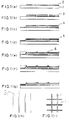
- a coloured layer 3 (as shown in Fig. 4(b) is formed by electrodeposition over a conductive film 2 (as shown in Fig. 4(a)) having an arbitrary pattern.
- a negative type photosensitive resin 7 having black pigments dispersed therein is applied (as shown in Fig. 4(c)).
- the substrate usually glass, has its back exposed (as shown in Fig. 4 (c)) by using the coloured layer as a photo mask.
- a transparent conductive film 4 is formed (as shown in Fig. 4 (e)).
- Liquid crystal displays of the thin film technology type have been expected in recent years to have a promising future.
- a shielding film is required to improve its shielding efficiency so as to prevent optical leakage when used as a switching element.
- the shielding film is required to have a lattice-shaped pattern.
- black pigment is dispersed in the resist so that the shielding film can only be added in limited amounts and thereby fails to have the required shielding efficiency. Since, moreover, the shielding film is formed by the exposure of the substrate back using the coloured layer as the mask, there arises a problem in that it is difficult to form the shielding film into the lattice shape.
- an object of the present invention to solve the above-specified problem of the prior art and to provide a process for manufacturing a multi-colour pattern having a shielding film which has a high shielding efficiency and can be formed into an arbitrary pattern shape.
- a colour filter comprising:
- the shielding film used is exemplified by the metal film so that a high shielding efficiency can be achieved. Since, moreover, the metal film can be easily patterned into an arbitrary shape by a lift-off method or an etching method, it is possible to form a shielding film having a pattern shape suited for a variety of display device systems.
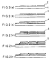
- Fig. 1 is a first example of the present invention for producing a colour filter.
- Fig. 2 is a second example of the present invention for producing a colour filter.
- Fig. 3 is a third example of the present invention for producing a colour filter
- Fig. 4 illustrates the prior art.
- Fig. 1 shows a first example of manufacturing a colour filter and is as follows:
- a shielding film having a shielding efficiency of 100% and a lattice-shaped pattern can be formed remarkably simply so as to realise a remarkably convenient multi-colour pattern manufacturing process together with electrodeposition.
- Fig. 2 shows a second example of manufacturing a colour filter and the steps are as follows:
- This example is a process for patterning the metal film using a lift-off method and so can dispense with etching the metal film. In contrast to the first example this simplifies the manufacturing more.
- Fig. 3 shows a third example of manufacturing a colour filter, the steps of which are as follows:
- the multi-colour pattern is more effective when the colour filter is used as a display device than those of the foregoing examples.
- a SiO 2 film was formed before formation of the further ITO film 4 of any of the foregoing examples by a sputtering method. As a result, contact of the ITO film 4 was improved. Similar results were obtained by an inorganic film other than the SiO 2 film.
- the metal film is formed as the shielding film.
- improvements in the shielding efficiency of the shielding film which has been impossible in the prior art, and has the capability of forming the shielding film in an arbitrary pattern. Since, moreover the first ITO film and the metal film are laminated, another effect is that the later ITO film is laminated, another effect is that the ITO film can have its final resistance reduced by the metal film even if ordinarily it has a high resistance.
- the ITO film can be thinned, it is possible to improve the transparency of the ITO film and to shorten the time period for forming the ITO film.
- the former can lead to an improvement in the quality of the multi-colour pattern itself, and the latter can contribute to a reduction in the cost of manufacturing.
Landscapes
- Physics & Mathematics (AREA)
- General Physics & Mathematics (AREA)
- Nonlinear Science (AREA)
- Mathematical Physics (AREA)
- Chemical & Material Sciences (AREA)
- Crystallography & Structural Chemistry (AREA)
- Optics & Photonics (AREA)
- Optical Filters (AREA)
- Liquid Crystal (AREA)
Applications Claiming Priority (2)
| Application Number | Priority Date | Filing Date | Title |
|---|---|---|---|
| JP30464/91 | 1991-02-25 | ||
| JP3030464A JPH04269713A (ja) | 1991-02-25 | 1991-02-25 | 多色パターンの製造方法 |
Publications (2)
| Publication Number | Publication Date |
|---|---|
| EP0501657A1 EP0501657A1 (en) | 1992-09-02 |
| EP0501657B1 true EP0501657B1 (en) | 1998-06-24 |
Family
ID=12304609
Family Applications (1)
| Application Number | Title | Priority Date | Filing Date |
|---|---|---|---|
| EP92301330A Expired - Lifetime EP0501657B1 (en) | 1991-02-25 | 1992-02-19 | Method of manufacturing a colour filter |
Country Status (6)
| Country | Link |
|---|---|
| US (1) | US6203950B1 (Sortimente) |
| EP (1) | EP0501657B1 (Sortimente) |
| JP (1) | JPH04269713A (Sortimente) |
| KR (1) | KR100276861B1 (Sortimente) |
| DE (1) | DE69225987T2 (Sortimente) |
| TW (1) | TW216830B (Sortimente) |
Families Citing this family (3)
| Publication number | Priority date | Publication date | Assignee | Title |
|---|---|---|---|---|
| JPH07294725A (ja) * | 1994-03-01 | 1995-11-10 | Seiko Instr Inc | カラーフィルター及び多色液晶表示装置の製造方法 |
| RU2226293C2 (ru) * | 2001-10-02 | 2004-03-27 | ОПТИВА, Инк. | Панель дисплея и многослойная пластина для ее изготовления |
| CN105527747A (zh) | 2016-02-18 | 2016-04-27 | 京东方科技集团股份有限公司 | 彩膜基板及其制作方法、显示面板、显示装置 |
Family Cites Families (11)
| Publication number | Priority date | Publication date | Assignee | Title |
|---|---|---|---|---|
| NL8105071A (nl) * | 1981-11-10 | 1983-06-01 | Philips Nv | Kleurenbeeldopneeminrichting. |
| US4522691A (en) | 1982-12-22 | 1985-06-11 | Seiko Instruments & Electronics Ltd. | Method for manufacturing a multicolor filter and a multicolor display device |
| JPS6033506A (ja) | 1983-08-04 | 1985-02-20 | Seiko Instr & Electronics Ltd | カラ−固体撮像素子の製造方法 |
| EP0226218B1 (en) | 1985-12-18 | 1993-07-14 | Canon Kabushiki Kaisha | Liquid crystal device |
| JP2640097B2 (ja) | 1986-03-20 | 1997-08-13 | セイコー電子工業株式会社 | 多色表示装置 |
| JPS6432233A (en) * | 1987-07-28 | 1989-02-02 | Sharp Kk | Liquid crystal display device |
| JP2593670B2 (ja) * | 1987-11-26 | 1997-03-26 | セイコー電子工業株式会社 | カラー表示装置の製造方法 |
| JPH01170902A (ja) * | 1987-12-25 | 1989-07-06 | Seiko Instr & Electron Ltd | カラーフィルターの製造方法 |
| EP0326112B1 (en) * | 1988-01-29 | 1994-09-14 | Toppan Printing Co., Ltd. | Electrode plate for display device and method for preparation thereof |
| EP0338412B2 (en) * | 1988-04-21 | 2000-05-10 | Asahi Glass Company Ltd. | Color liquid crystal display device and method for driving same |
| JPH0322221U (Sortimente) * | 1989-07-14 | 1991-03-07 |
-
1991
- 1991-02-25 JP JP3030464A patent/JPH04269713A/ja active Pending
-
1992
- 1992-02-19 DE DE69225987T patent/DE69225987T2/de not_active Expired - Fee Related
- 1992-02-19 EP EP92301330A patent/EP0501657B1/en not_active Expired - Lifetime
- 1992-02-24 US US07/840,345 patent/US6203950B1/en not_active Expired - Fee Related
- 1992-02-25 KR KR1019920002902A patent/KR100276861B1/ko not_active Expired - Fee Related
- 1992-04-17 TW TW081101481A patent/TW216830B/zh active
Also Published As
| Publication number | Publication date |
|---|---|
| EP0501657A1 (en) | 1992-09-02 |
| US6203950B1 (en) | 2001-03-20 |
| DE69225987T2 (de) | 1998-10-22 |
| KR100276861B1 (ko) | 2001-01-15 |
| TW216830B (Sortimente) | 1993-12-01 |
| JPH04269713A (ja) | 1992-09-25 |
| DE69225987D1 (de) | 1998-07-30 |
Similar Documents
| Publication | Publication Date | Title |
|---|---|---|
| TWI237726B (en) | Active matrix substrate having column spacers integral with protective layer and process for fabrication thereof | |
| EP0905544B1 (en) | A method of fabricating a liquid crystal display | |
| US6057900A (en) | Color liquid crystal display device and method for producing color filter substrate | |
| CA2352168C (en) | Color filters for flat panel displays | |
| KR100236613B1 (ko) | 액티브 매트릭스 액정표시 장치의 블랙 매트릭스 제조 방법 | |
| EP0631171B1 (en) | Method of manufacturing a liquid crystal display device | |
| EP0501657B1 (en) | Method of manufacturing a colour filter | |
| JPH0687084B2 (ja) | カラーフイルタの製造方法 | |
| KR100670062B1 (ko) | 액정 표시 장치용 색 필터 기판 및 그 제조 방법 | |
| JPH07248412A (ja) | カラーフィルタとカラーフィルタの製造方法 | |
| JP2000162643A (ja) | 液晶表示装置及びその製造方法 | |
| JP4369543B2 (ja) | カラーフィルタおよびその製造方法 | |
| JPH10177109A (ja) | カラーフィルタおよびその製造方法 | |
| EP0387805B1 (en) | Method of manufacturing liquid crystal display device | |
| JPH04355406A (ja) | カラーフィルタとその製造方法 | |
| KR100433660B1 (ko) | 액정표시소자및그제조방법 | |
| JPH08278497A (ja) | カラーフィルタおよびその製造方法 | |
| JPH06331818A (ja) | カラーフィルタ | |
| CN108845447A (zh) | 彩色滤光结构、彩色滤光结构的制造方法及光刻制程 | |
| KR960009378Y1 (ko) | 액정 디스플레이용 칼라필터 기판의 구조 | |
| JP2626668B2 (ja) | 表面着色体の製造方法 | |
| JPH09258206A (ja) | カラーフィルタ層付駆動基板の製造方法 | |
| JP2000347021A (ja) | カラーフィルタおよびその製造方法 | |
| KR970002981B1 (ko) | 액정 디스플레이용 컬러필터의 제조방법 | |
| KR101017205B1 (ko) | 칼라 필터가 형성된 박막 트랜지스터 기판 및 그 제조 방법 |
Legal Events
| Date | Code | Title | Description |
|---|---|---|---|
| PUAI | Public reference made under article 153(3) epc to a published international application that has entered the european phase |
Free format text: ORIGINAL CODE: 0009012 |
|
| AK | Designated contracting states |
Kind code of ref document: A1 Designated state(s): DE FR GB IT NL |
|
| 17P | Request for examination filed |
Effective date: 19930227 |
|
| 17Q | First examination report despatched |
Effective date: 19960902 |
|
| GRAG | Despatch of communication of intention to grant |
Free format text: ORIGINAL CODE: EPIDOS AGRA |
|
| GRAG | Despatch of communication of intention to grant |
Free format text: ORIGINAL CODE: EPIDOS AGRA |
|
| GRAH | Despatch of communication of intention to grant a patent |
Free format text: ORIGINAL CODE: EPIDOS IGRA |
|
| GRAH | Despatch of communication of intention to grant a patent |
Free format text: ORIGINAL CODE: EPIDOS IGRA |
|
| GRAA | (expected) grant |
Free format text: ORIGINAL CODE: 0009210 |
|
| AK | Designated contracting states |
Kind code of ref document: B1 Designated state(s): DE FR GB IT NL |
|
| REF | Corresponds to: |
Ref document number: 69225987 Country of ref document: DE Date of ref document: 19980730 |
|
| ET | Fr: translation filed | ||
| REG | Reference to a national code |
Ref country code: FR Ref legal event code: TP |
|
| PLBE | No opposition filed within time limit |
Free format text: ORIGINAL CODE: 0009261 |
|
| 26N | No opposition filed | ||
| REG | Reference to a national code |
Ref country code: GB Ref legal event code: IF02 |
|
| PGFP | Annual fee paid to national office [announced via postgrant information from national office to epo] |
Ref country code: FR Payment date: 20030210 Year of fee payment: 12 |
|
| PGFP | Annual fee paid to national office [announced via postgrant information from national office to epo] |
Ref country code: GB Payment date: 20030219 Year of fee payment: 12 |
|
| PGFP | Annual fee paid to national office [announced via postgrant information from national office to epo] |
Ref country code: NL Payment date: 20030226 Year of fee payment: 12 |
|
| PGFP | Annual fee paid to national office [announced via postgrant information from national office to epo] |
Ref country code: DE Payment date: 20030227 Year of fee payment: 12 |
|
| PG25 | Lapsed in a contracting state [announced via postgrant information from national office to epo] |
Ref country code: GB Free format text: LAPSE BECAUSE OF NON-PAYMENT OF DUE FEES Effective date: 20040219 |
|
| PG25 | Lapsed in a contracting state [announced via postgrant information from national office to epo] |
Ref country code: NL Free format text: LAPSE BECAUSE OF NON-PAYMENT OF DUE FEES Effective date: 20040901 Ref country code: DE Free format text: LAPSE BECAUSE OF NON-PAYMENT OF DUE FEES Effective date: 20040901 |
|
| GBPC | Gb: european patent ceased through non-payment of renewal fee |
Effective date: 20040219 |
|
| PG25 | Lapsed in a contracting state [announced via postgrant information from national office to epo] |
Ref country code: FR Free format text: LAPSE BECAUSE OF NON-PAYMENT OF DUE FEES Effective date: 20041029 |
|
| NLV4 | Nl: lapsed or anulled due to non-payment of the annual fee |
Effective date: 20040901 |
|
| REG | Reference to a national code |
Ref country code: FR Ref legal event code: ST |
|
| PG25 | Lapsed in a contracting state [announced via postgrant information from national office to epo] |
Ref country code: IT Free format text: LAPSE BECAUSE OF NON-PAYMENT OF DUE FEES Effective date: 20050219 |