EP0501481B1 - Schaltung zur Stromsteuerung - Google Patents
Schaltung zur Stromsteuerung Download PDFInfo
- Publication number
- EP0501481B1 EP0501481B1 EP92103374A EP92103374A EP0501481B1 EP 0501481 B1 EP0501481 B1 EP 0501481B1 EP 92103374 A EP92103374 A EP 92103374A EP 92103374 A EP92103374 A EP 92103374A EP 0501481 B1 EP0501481 B1 EP 0501481B1
- Authority
- EP
- European Patent Office
- Prior art keywords
- mosfet
- node
- control circuit
- current control
- gate
- Prior art date
- Legal status (The legal status is an assumption and is not a legal conclusion. Google has not performed a legal analysis and makes no representation as to the accuracy of the status listed.)
- Expired - Lifetime
Links
- 239000003990 capacitor Substances 0.000 claims description 19
- 230000000630 rising effect Effects 0.000 claims 1
- 230000014509 gene expression Effects 0.000 description 28
- 230000003247 decreasing effect Effects 0.000 description 8
- 238000010586 diagram Methods 0.000 description 6
- 102220124597 rs374821619 Human genes 0.000 description 1
- 230000002747 voluntary effect Effects 0.000 description 1
Images




Classifications
-
- H—ELECTRICITY
- H03—ELECTRONIC CIRCUITRY
- H03K—PULSE TECHNIQUE
- H03K17/00—Electronic switching or gating, i.e. not by contact-making and –breaking
- H03K17/16—Modifications for eliminating interference voltages or currents
- H03K17/161—Modifications for eliminating interference voltages or currents in field-effect transistor switches
- H03K17/162—Modifications for eliminating interference voltages or currents in field-effect transistor switches without feedback from the output circuit to the control circuit
- H03K17/163—Soft switching
-
- G—PHYSICS
- G11—INFORMATION STORAGE
- G11B—INFORMATION STORAGE BASED ON RELATIVE MOVEMENT BETWEEN RECORD CARRIER AND TRANSDUCER
- G11B5/00—Recording by magnetisation or demagnetisation of a record carrier; Reproducing by magnetic means; Record carriers therefor
- G11B5/02—Recording, reproducing, or erasing methods; Read, write or erase circuits therefor
- G11B5/09—Digital recording
Definitions
- This invention relates to a current control circuit, and more particularly to, a current control circuit used for a magnetic head of a tape recorder.
- a tape recorder includes a magnetic head, a switch connected to a power supply for applying a predetermined voltage to the magnetic head, and a current control circuit for controlling amount of current flowing through the magnetic head.
- the current control circuit includes a p-MOSFET connected at a drain to a first node, at a gate to an input terminal and at a source to a power supply, an n-MOSFET connected at a drain to the first node, at a gate to the input terminal and at a source to ground, an n-MOSFET connected at a drain to an output terminal, at a gate to a second node and at a source to ground, a resistor connected between the first node and the second node, and a capacitor connected between the second node and ground.
- a reproducing circuit In a reproducing mode, a reproducing circuit has positive and negative threshold levels for detecting a recorded data.
- the positive and negative threshold levels are set to be intermediate values between high level data and low level data on the positive and negative sides, respectively.
- the magnetic head detects the magnetic data of the magnetic tape which is then compared with the threshold levels in the reproducing circuit.
- the threshold levels of the magnetic data reproduction are different between the positive and negative sides, because the absolute values of low level data are different between the positive and negative sides for the reason that the changing rates of currents flowing through the magnetic head are different between the positive and negative sides due to a circuit structure of the current controller. This will be explained in more detail later. Therefore, noise margins become different between the positive and negative sides, so that operation of the magnetic data reproduction is unstable. Further, it is necessary in the reproducing circuit to be provided with two different detectors each having a different threshold level for detecting a corresponding side of positive and negative levels, so that structure of the reproducing circuit including the magnetic head becomes complicated.
- the threshold levels of the magnetic head are set to be the same level, if a resistance of a resistor and a capacitance of a capacitor are set to be sufficient high in the current controller to equalize the current changing rates on the positive and negative sides.
- a large space is necessary for the large resistor and the large capacitor, so that the current control circuit is difficult to be fabricated compactly.
- JP-A-1276402 discloses a current controller for controlling the current through a magnetic head. According to this current controller the current through the magnetic head is controlled so that the current rises and falls with the same changing rate.
- a current control circuit includes the features set forth in claims 1 and 4, respectively.
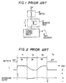
- Fig. 1 shows a tape recorder 10 of a general type for recording a predetermined digital data on a magnetic tape (not shown) and reproducing the recorded data from the magnetic tape.
- the tape recorder 10 includes a magnetic head 12, a switch 14 connected to a power supply V cc for applying a predetermined voltage to the magnetic head 12, and a current control circuit 16 for controlling current "I" flowing through the magnetic head 12.
- Fig. 2 shows timing chart of the tape recorder 10.
- digital data having a level corresponding to a changing rate of the current "I" is recorded on the magnetic tape.
- positive data of high level is recorded at the initial stage of the time T1
- negative data of high level is recorded at the initial stage of the time T4
- negative data of low level is recorded for the time T2
- positive data of low level is recorded for the time T3.
- the recorded data is reproduced to be the same level as the recording level.
- the changing rate of the current "I" is changed by the current control circuit 16, so that it is possible that a voluntary data is recorded on a magnetic tape. And, the recorded data can be reproduced from the magnetic tape by detecting level and polarity of the recorded data.
- Fig. 3 shows the current control circuit 16 as mentioned above.
- the current control circuit 16 includes a p-MOSFET 20 connected at a drain to a first node 22, at a gate to an input terminal IN and at a source to a power supply V cc , an n-MOSFET 24 connected at a drain to the first node 22, at a gate to the input terminal IN and at a source to ground GND, an n-MOSFET 26 connected at a drain to an output terminal OUT, at a gate to a second node 32, and at a source to ground GND, a resistor 28 connected between the first node 22 and the second node 32, and a capacitor 30 connected between the second node 32 and ground GND.
- V Cf V CC (e -1/c30 ⁇ R28 )
- the current "I" flowing through the n-MOSFET 26 can be calculated by the below expressions (4a) and (4b) on condition that the n-MOSFET 26 is operating in a saturation region thereof.
- I 0 : (V CS ⁇ V TN )
- I ( ⁇ N /2)(V Cf - V TN ) 2
- V Cf > V TN ) ( ⁇ N /2)[V CC (e -1/c30 ⁇ R28 ) - V TN ] 2
- a changing rate (dI/dt) of the current "I" is set to be low at each side of positive and negative sides by setting value of the resistor 28 and the capacitor 30 to be high, respectively.
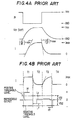
- a ratio "R” of the absolute value of "(dI/dt)f ⁇ max" to "(dI/dt)r ⁇ max" can be calculated by the below expression (7).
- positive and negative threshold levels VS1 and VS2 are determined to be intermediate value between a high level H r and the low level L r , and between a high level H f and the low level L f , respectively, as shown in Fig. 4B.
- the threshold levels VS1 and VS2 are determined to be different values in the magnetic head 12, so that noise margins are different between the positive and negative sides. As a result operation of the magnetic head 12 becomes unstable. Further, it is necessary in a reproducing circuit to be provided with two different detectors each having a different detecting level for detecting a corresponding side of positive and negative data, so that structure of the reproducing circuit including the magnetic head 12 becomes complicated.
- the threshold levels VS1 and VS2 are set to be the same level.
- the large resistor and the large capacitor necessitates large space, so that the current control circuit 16 is difficult to be fabricated compactly.
- Fig. 5 shows a current control circuit 36 of a first preferred embodiment according to the invention.
- the current control circuit 36 includes a p-MOSFET 40 connected at a drain to a first node 42, at a gate to an input terminal IN and at a source to a power supply V CC , an n-MOSFET 44 connected at a drain to the first node 42, at a gate to the input terminal IN and at a source to ground GND, a resistor 45 connected between the first connecting point 42 and the drain of the n-MOSFET 44, an n-MOSFET 46 connected at a drain to an output terminal OUT, at a gate to a second node 52 and at a source to ground GND, a resistor 48 connected between the first node 22 and the second node 52, and a capacitor 50 connected between the second node 32 and ground GND.
- a voltage V Ar at the second node 52 that is a gate voltage of the n-MOSFET 46 can be calculated by the below expression (8) on condition that a resistance R48 of the resistor 48 is sufficiently larger than an on resistance of the p-MOSFET 40.
- C50 indicates a capacitance of the capacitor 50.
- V Ar V CC [1- e( -1/c50 ⁇ R48) ]
- I current flowing through the n-MOSFET 46 can be calculated by the below expressions (9a) and (9b) using a gain constant " ⁇ N " of an n-MOSFET and a threshold voltage "V TN " of an n-MOSFET, on condition that the n-MOSFET 46 is operating in a saturation region thereof.
- a voltage V Af at the second node 52 that is the gate voltage of the n-MOSFET 46 can be calculated by the below expression (10) on condition that a total resistance R45+ R48 of the resistors 45 and 48 is sufficiently larger than an on-resistance of the n-MOSFET 44.
- V Af V CC [e -1/c50(R45+R48) ]
- the current "I" flowing through the n-MOSFET 46 can be calculated by the below expressions (11a) and (11b) on condition that the n-MOSFET 46 is operating in a saturation region thereof.
- I 0 : (V Af ⁇ V TN )
- I ( ⁇ N /2) (V Af - V TN ) 2
- V Af > V TN ) ( ⁇ N /2) [V cc (e -1/c50(R45+R48) ) - V TN ] 2
- changing rate (dI/dt) of the current "I" can be determined to be low easily by controlling values of the resistors 45 and 48 and the capacitor 50, respectively.
- a ratio "R” of the absolute value of "(dI/dt)f ⁇ max" to "(dI/dt)r ⁇ max" can be calculated by the below expression (14).
- the current control circuit 36 even if the capacitor 50 is connected between the second node 52 and the power supply V CC , the current control circuit 36 operates in the same manner as in the aforementioned circuit shown in Fig. 5.
- Fig. 7 shows a current control circuit 56 of a second preferred embodiment according to the invention.
- explanation of structure corresponding to that of the first preferred embodiment is omitted.
- the current control circuit 56 includes a switch 58 connected between a resistor 48 and a second node 52, a p-MOSFET 60 connected at a drain to the second node 52 and at a source to a power supply V cc , and an n-MOSFET 62 connected at a drain to the second node 62 and at a source to ground GND.
- the switch 58 includes an n-MOSFET 65 supplied at a gate with a control signal S1 and a p-MOSFET 63 supplied at a gate with an inverted signal S1 ⁇ of the signal S1.
- the p-MOSFET 60 and the n-MOSFET 62 are supplied at gates with control signals S2 and S3, respectively.
- both of low level data and high level data of positive and negative sides can be supplied. If high level data of positive side is not necessary, the p-MOSFET 60 can be omitted. And, if high level data of negative side is not necessary, the n-MOSFET 62 can be omitted.
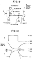
- Fig. 9 shows a current control circuit 66 of a third preferred embodiment according to the invention.
- the current control circuit 66 has a much similar structure to the current control circuit 34 of the first preferred embodiment, so that explanation of corresponding components is omitted.
- the current control circuit 66 includes a resistor 67 connected between a first node 68 and a drain of a p-MOSFET 40, and a p-MOSFET 70 connected at a source to a power supply V cc , at a drain to an output terminal OUT and at a gate to a second node 72.
- a voltage level at the input terminal IN changes from low to high on condition that a resistance R48 of a resistor 48 is sufficiently larger than an on-resistance of the n-MOSFET 44
- a voltage V Bf at the second node 72 that is a gate voltage of the p-MOSFET 70 can be calculated by the below expression (16).
- V Bf V CC (e -1/c50 ⁇ R48 )
- current "I" flowing through the p-MOSFET 70 can be calculated by the below expressions (17a) and (17b) using a gain constant ⁇ P "of a p-MOSFET and a threshold voltage "V TP " of a p-MOSFET, on condition that the p-MOSFET 70 is operating in a saturation region thereof.
- ⁇ P indicates a gain constant of a p-MOSFET
- V TP indicates a threshold voltage of a P-MOSFET.
- V Br V CC [1 - e -1/c50(R67+R48) ]
- the current "I" flowing through the p-MOSFET 70 on condition that the p-MOSFET 70 is operating in a saturation region thereof, can be calculated by the below expressions (19a) and (19b).
- I 0 : (V CC - V Br ⁇ V TP )
- I ( ⁇ P /2)(V CC - V Br - V TP ) 2 : (V CC - V Br )>
- V TP ( ⁇ P /2)[V CC (e -1/c50(R67+R48) ) - V TP ] 2
- changing rate (dI/dt) of the current "I" can be determined to be low easily by controlling values of the resistors 67 and 48 and the capacitor 50, respectively.
- a ratio "R” of the absolute value of "(dI/dt)f ⁇ max" to "(dI/dt)r ⁇ max” can be calculated by the below expression (22).
- the maximum changing rate "(dI/dt)r ⁇ max" in a gradually increasing state and the maximum changing rate "(dI/dt)f ⁇ max" in a gradually decreasing state can be set the same value by controlling the resistances R67 and R48 so that the ratio "R" becomes 1.
- Fig. 11 shows a current control circuit 76 of a fourth preferred embodiment according to the invention.
- explanation of structure corresponding to those of the second and third preferred embodiments is omitted.
- the current control circuit 76 includes a switch 58 connected between a resistor 48 and a second node 52, and a p-MOSFET 78 connected at a drain to the second node 52 and at a source to a power supply V CC .
- the p-MOSFET 78 is supplied at gate with control signal S2.
Landscapes
- Electronic Switches (AREA)
- Digital Magnetic Recording (AREA)
Claims (6)
- Stromsteuerschaltung mit:einem ersten MOSFET (40) von einem ersten Leitfähigkeitstyp, der mit seinem Drain mit einem ersten Knoten (42) verbunden ist, mit seinem Gate mit einem Eingangsanschluß (IN) und mit seiner Source mit einem ersten Spannungsversorgungsanschluß (Vcc);einem zweiten MOSFET (44) von einem zweiten Leitfähigkeitstyp, der mit seinem Drain mit dem ersten Knoten (42) verbunden ist, mit seinem Gate mit dem Eingangsanschluß (IN) und mit seiner Source mit einem zweiten Versorgungsspannungsanschluß (GND);einem dritten MOSFET (46) vom zweiten Leitfähigkeitstyp, der mit seinem Drain an einem Ausgangsanschluß (OUT) verbunden ist, mit seinem Gate mit dem ersten Knoten (42) über einen ersten Widerstand (48) und mit seiner Source mit dem zweiten Spannungsversorgungsanschluß (GND); undeinem Kondensator (50), der zwischen dem Gate des dritten MOSFET (46) und dem zweiten Spannungsversorgungsanschluß (GND) verbunden ist;gekennzeichnet durch
einen zweiten Widerstand (45), der zwischen dem Drain des zweiten MOSFET (44) und dem ersten Knoten (42) vorgesehen ist, wobei der erste und zweite Widerstand (48, 45) und der Kondensator (50) so gesetzt sind, daß die maximalen Ladegeschwindigkeiten der ansteigenden und abfallenden Ströme vom Ausgangsanschluß (OUT) über den dritten MOSFET (46) gleichgemacht sind. - Stromsteuerschaltung nach Anspruch 1,
dadurch gekennzeichnet, daß er weiter aufweist:
eine Schaltschaltung (58), die zwischen dem Gate des dritten MOSFET (46) und einem gemeinsamen Knoten des ersten Widerstands (48) und des Kondensators (50) verbunden ist. - Stromsteuerschaltung nach Anspruch 2,
dadurch gekennzeichnet, daß der Schaltschaltkreis (58) einen P-MOSFET (63) und einen N-MOSFET (65) aufweist. - Stromsteuerschaltung mit:einem ersten MOSFET (40) von einem ersten Leitfähigkeitstyp, der mit seinem Drain mit einem ersten Knoten (68) verbunden ist, mit seinem Gate mit einem Eingangsanschluß (IN) und mit seiner Source mit einem ersten Spannungsversorgungsanschluß (Vcc);einem zweiten MOSFET (44) von einem zweiten Leitfähigkeitstyp, der mit seinem Drain mit dem ersten Knoten (68) verbunden ist, mit seinem Gate mit dem Eingangsanschluß (IN) und mit seiner Source mit einem zweiten Spannungsversorgungsanschluß (GND);einem dritten MOSFET (70) vom ersten Leitfähigkeitstyp, der mit seinem Drain mit einem Ausgangsanschluß (OUT) verbunden ist, mit seinem Gate mit dem ersten Knoten (68) über einen ersten Widerstand (48) und mit seiner Source mit dem ersten Spannungsversorgungsanschluß (Vcc); undeinem Kondensator (50), der zwischen dem Gate des dritten MOSFET (70) und dem zweiten Spannungsversorgungsanschluß (GND) verbunden ist;gekennzeichnet durch
einen zweiten Widerstand (67), der zwischen den Drain des ersten MOSFET (40) und dem ersten Knoten (68) vorgesehen ist, wobei der erste und zweite Widerstand (48, 67) und der Kondensator (50) so gesetzt sind, daß die maximale Ladungsgeschwindigkeit der ansteigenden und abfallenden Ströme von dem Ausgangsanschluß über den dritten MOSFET gleichgemacht werden. - Stromsteuerschaltung nach Anspruch 4,
dadurch gekennzeichnet, daß er ferner aufweist einen Schaltschaltkreis (58), der zwischen dem Gate des dritten MOSFET (70) und einem gemeinsamen Knoten des ersten Widerstands und des Kondensators geschaltet ist. - Stromsteuerschaltung nach Anspruch 5,
dadurch gekennzeichnet, daß der Schaltschaltkreis (58) einen P-MOSFET (63) und einen N-MOSFET (65) aufweist.
Applications Claiming Priority (2)
| Application Number | Priority Date | Filing Date | Title |
|---|---|---|---|
| JP34310/91 | 1991-02-28 | ||
| JP3034310A JP2932722B2 (ja) | 1991-02-28 | 1991-02-28 | 電流駆動回路 |
Publications (3)
| Publication Number | Publication Date |
|---|---|
| EP0501481A2 EP0501481A2 (de) | 1992-09-02 |
| EP0501481A3 EP0501481A3 (en) | 1993-03-17 |
| EP0501481B1 true EP0501481B1 (de) | 1997-04-23 |
Family
ID=12410591
Family Applications (1)
| Application Number | Title | Priority Date | Filing Date |
|---|---|---|---|
| EP92103374A Expired - Lifetime EP0501481B1 (de) | 1991-02-28 | 1992-02-27 | Schaltung zur Stromsteuerung |
Country Status (4)
| Country | Link |
|---|---|
| US (1) | US5281870A (de) |
| EP (1) | EP0501481B1 (de) |
| JP (1) | JP2932722B2 (de) |
| DE (1) | DE69219188T2 (de) |
Families Citing this family (13)
| Publication number | Priority date | Publication date | Assignee | Title |
|---|---|---|---|---|
| GB9414261D0 (en) * | 1994-07-14 | 1994-08-31 | Motorola Gmbh | MOS N-channel transistor protection |
| JP3229164B2 (ja) * | 1994-07-28 | 2001-11-12 | インターナショナル・ビジネス・マシーンズ・コーポレーション | ラッチ回路 |
| US5514995A (en) * | 1995-01-30 | 1996-05-07 | Micrel, Inc. | PCMCIA power interface |
| DE69521028T2 (de) * | 1995-03-29 | 2001-09-06 | Agilent Technologies, Inc. | Vortreiberschaltung zum rauscharmen Schalten hoher Ströme in einer Last |
| US5650744A (en) * | 1996-02-20 | 1997-07-22 | Vlsi Technology, Inc. | Charge neutralizing system for circuits having charge injection problems and method therefor |
| DE10064123B4 (de) | 2000-12-21 | 2004-11-18 | Infineon Technologies Ag | Schaltungsanordnung zur Ansteuerung eines Halbleiterschaltelements |
| US6753708B2 (en) * | 2002-06-13 | 2004-06-22 | Hewlett-Packard Development Company, L.P. | Driver circuit connected to pulse shaping circuitry and method of operating same |
| US20040246039A1 (en) * | 2003-06-03 | 2004-12-09 | Chi-Ming Hsiao | Switched capacitor circuit capable of minimizing clock feedthrough effect in a voltage controlled oscillator circuit |
| JP2008193144A (ja) * | 2007-01-31 | 2008-08-21 | Mitsumi Electric Co Ltd | サーマルヘッド駆動回路 |
| JP2008306618A (ja) * | 2007-06-11 | 2008-12-18 | Nissan Motor Co Ltd | 電圧駆動型素子を駆動するための駆動回路 |
| US8525575B2 (en) * | 2010-11-12 | 2013-09-03 | Fairchild Semiconductor Corporation | Pass transistor capacitance and jitter reduction |
| FR2985115B1 (fr) * | 2011-12-21 | 2014-03-07 | Continental Automotive France | Commande d'une charge inductive avec mecanisme de reduction de courant sensible a la temperature |
| JP6716419B2 (ja) * | 2015-11-30 | 2020-07-01 | ルネサスエレクトロニクス株式会社 | 送信回路および通信回路 |
Family Cites Families (9)
| Publication number | Priority date | Publication date | Assignee | Title |
|---|---|---|---|---|
| JPS5453955A (en) * | 1977-10-07 | 1979-04-27 | Hitachi Ltd | Driving circuit |
| GB2163589B (en) * | 1984-07-20 | 1987-11-25 | Victor Company Of Japan | Control system for controlling multi-track recording head device |
| KR900004191B1 (ko) * | 1987-03-18 | 1990-06-18 | 삼성전자 주식회사 | Rc시정수를 이용한 가변 클럭 지연회로 |
| JPH01240013A (ja) * | 1988-03-22 | 1989-09-25 | Hitachi Ltd | 半導体集積回路装置 |
| JP2736789B2 (ja) * | 1988-09-24 | 1998-04-02 | 三菱電機株式会社 | ドライバ回路装置 |
| JPH0292017A (ja) * | 1988-09-28 | 1990-03-30 | Nec Corp | 出力回路 |
| US5068553A (en) * | 1988-10-31 | 1991-11-26 | Texas Instruments Incorporated | Delay stage with reduced Vdd dependence |
| US5120999A (en) * | 1991-02-08 | 1992-06-09 | Texas Instruments Incorporated | Output-buffer noise-control circuit |
| US5120992A (en) * | 1991-07-03 | 1992-06-09 | National Semiconductor Corporation | CMOS output driver with transition time control circuit |
-
1991
- 1991-02-28 JP JP3034310A patent/JP2932722B2/ja not_active Expired - Fee Related
-
1992
- 1992-02-27 EP EP92103374A patent/EP0501481B1/de not_active Expired - Lifetime
- 1992-02-27 DE DE69219188T patent/DE69219188T2/de not_active Expired - Fee Related
- 1992-02-28 US US07/843,553 patent/US5281870A/en not_active Expired - Fee Related
Also Published As
| Publication number | Publication date |
|---|---|
| JP2932722B2 (ja) | 1999-08-09 |
| EP0501481A2 (de) | 1992-09-02 |
| EP0501481A3 (en) | 1993-03-17 |
| US5281870A (en) | 1994-01-25 |
| DE69219188D1 (de) | 1997-05-28 |
| JPH04273613A (ja) | 1992-09-29 |
| DE69219188T2 (de) | 1997-11-20 |
Similar Documents
| Publication | Publication Date | Title |
|---|---|---|
| US5869988A (en) | High speed write driver for inductive heads | |
| EP0501481B1 (de) | Schaltung zur Stromsteuerung | |
| US5880626A (en) | Active damping for a disk drive write circuit | |
| JP2749729B2 (ja) | 磁気記録再生回路 | |
| US5300837A (en) | Delay compensation technique for buffers | |
| US6297921B1 (en) | Write driver circuit having programmable overshoot and undershoot | |
| US5297024A (en) | Voice coil driver with variable gain in seek and track-follow modes | |
| US4873673A (en) | Driver circuit having a current mirror circuit | |
| US6429987B1 (en) | High speed inductor current driver with minimum overshoot | |
| US5724201A (en) | Method and apparatus for reducing transition time for a magnetic head to switch from a write made to a read mode by reducing a maximum current value at different rates | |
| US6215607B1 (en) | Write driver using continuous damping network to reduce overshoot, undershoot and settling time for magnetic inductive recording head | |
| US6671113B2 (en) | Characteristically terminated write driver with compensation for magnetic response and method therefor | |
| EP1187102A2 (de) | Verfahren zum differentielem Schreiben auf einer Speicherplatte | |
| JPH08501438A (ja) | パルス信号を用いた制御方法及び装置 | |
| JP3283389B2 (ja) | 磁気記録回路 | |
| US20050218983A1 (en) | Differential amplifier | |
| US6920002B2 (en) | Reproducing amplifier and magnetic recording and reproducing apparatus employing the reproducing amplifier | |
| JPH0345474B2 (de) | ||
| US6580238B2 (en) | Motor driver | |
| US5331477A (en) | Low voltage, constant current magnetic transducer drive system for digital recording | |
| EP0366489A2 (de) | NAND Gateschaltungen | |
| US6594097B1 (en) | Reproduction amplifier circuit of hard disk drive | |
| JP2003272105A (ja) | 磁気ヘッド駆動用ライトドライバー回路 | |
| JP2001084505A (ja) | 電流ドライバ回路 | |
| JP3526103B2 (ja) | 電圧検出器のヒステリシス回路 |
Legal Events
| Date | Code | Title | Description |
|---|---|---|---|
| PUAI | Public reference made under article 153(3) epc to a published international application that has entered the european phase |
Free format text: ORIGINAL CODE: 0009012 |
|
| 17P | Request for examination filed |
Effective date: 19920227 |
|
| AK | Designated contracting states |
Kind code of ref document: A2 Designated state(s): DE FR GB NL |
|
| PUAL | Search report despatched |
Free format text: ORIGINAL CODE: 0009013 |
|
| AK | Designated contracting states |
Kind code of ref document: A3 Designated state(s): DE FR GB NL |
|
| 17Q | First examination report despatched |
Effective date: 19960126 |
|
| GRAG | Despatch of communication of intention to grant |
Free format text: ORIGINAL CODE: EPIDOS AGRA |
|
| GRAH | Despatch of communication of intention to grant a patent |
Free format text: ORIGINAL CODE: EPIDOS IGRA |
|
| GRAH | Despatch of communication of intention to grant a patent |
Free format text: ORIGINAL CODE: EPIDOS IGRA |
|
| GRAA | (expected) grant |
Free format text: ORIGINAL CODE: 0009210 |
|
| AK | Designated contracting states |
Kind code of ref document: B1 Designated state(s): DE FR GB NL |
|
| REF | Corresponds to: |
Ref document number: 69219188 Country of ref document: DE Date of ref document: 19970528 |
|
| ET | Fr: translation filed | ||
| PLBE | No opposition filed within time limit |
Free format text: ORIGINAL CODE: 0009261 |
|
| STAA | Information on the status of an ep patent application or granted ep patent |
Free format text: STATUS: NO OPPOSITION FILED WITHIN TIME LIMIT |
|
| 26N | No opposition filed | ||
| REG | Reference to a national code |
Ref country code: GB Ref legal event code: IF02 |
|
| PGFP | Annual fee paid to national office [announced via postgrant information from national office to epo] |
Ref country code: FR Payment date: 20030210 Year of fee payment: 12 |
|
| PGFP | Annual fee paid to national office [announced via postgrant information from national office to epo] |
Ref country code: NL Payment date: 20030226 Year of fee payment: 12 Ref country code: GB Payment date: 20030226 Year of fee payment: 12 |
|
| PGFP | Annual fee paid to national office [announced via postgrant information from national office to epo] |
Ref country code: DE Payment date: 20030306 Year of fee payment: 12 |
|
| REG | Reference to a national code |
Ref country code: GB Ref legal event code: 732E |
|
| NLS | Nl: assignments of ep-patents |
Owner name: NEC ELECTRONICS CORPORATION |
|
| REG | Reference to a national code |
Ref country code: FR Ref legal event code: TP |
|
| PG25 | Lapsed in a contracting state [announced via postgrant information from national office to epo] |
Ref country code: GB Free format text: LAPSE BECAUSE OF NON-PAYMENT OF DUE FEES Effective date: 20040227 |
|
| PG25 | Lapsed in a contracting state [announced via postgrant information from national office to epo] |
Ref country code: NL Free format text: LAPSE BECAUSE OF NON-PAYMENT OF DUE FEES Effective date: 20040901 Ref country code: DE Free format text: LAPSE BECAUSE OF NON-PAYMENT OF DUE FEES Effective date: 20040901 |
|
| GBPC | Gb: european patent ceased through non-payment of renewal fee | ||
| PG25 | Lapsed in a contracting state [announced via postgrant information from national office to epo] |
Ref country code: FR Free format text: LAPSE BECAUSE OF NON-PAYMENT OF DUE FEES Effective date: 20041029 |
|
| NLV4 | Nl: lapsed or anulled due to non-payment of the annual fee |
Effective date: 20040901 |
|
| REG | Reference to a national code |
Ref country code: FR Ref legal event code: ST |