EP0497358A1 - Dispositif optique intégré pour démultiplexage de plusieurs canaux de longueurs d'onde différents et méthode de sa fabrication - Google Patents
Dispositif optique intégré pour démultiplexage de plusieurs canaux de longueurs d'onde différents et méthode de sa fabrication Download PDFInfo
- Publication number
- EP0497358A1 EP0497358A1 EP92101575A EP92101575A EP0497358A1 EP 0497358 A1 EP0497358 A1 EP 0497358A1 EP 92101575 A EP92101575 A EP 92101575A EP 92101575 A EP92101575 A EP 92101575A EP 0497358 A1 EP0497358 A1 EP 0497358A1
- Authority
- EP
- European Patent Office
- Prior art keywords
- layer
- waveguide
- coupling
- optical
- diffraction grating
- Prior art date
- Legal status (The legal status is an assumption and is not a legal conclusion. Google has not performed a legal analysis and makes no representation as to the accuracy of the status listed.)
- Granted
Links
Images


Classifications
-
- G—PHYSICS
- G02—OPTICS
- G02B—OPTICAL ELEMENTS, SYSTEMS OR APPARATUS
- G02B6/00—Light guides; Structural details of arrangements comprising light guides and other optical elements, e.g. couplings
- G02B6/24—Coupling light guides
- G02B6/26—Optical coupling means
- G02B6/28—Optical coupling means having data bus means, i.e. plural waveguides interconnected and providing an inherently bidirectional system by mixing and splitting signals
- G02B6/293—Optical coupling means having data bus means, i.e. plural waveguides interconnected and providing an inherently bidirectional system by mixing and splitting signals with wavelength selective means
- G02B6/29304—Optical coupling means having data bus means, i.e. plural waveguides interconnected and providing an inherently bidirectional system by mixing and splitting signals with wavelength selective means operating by diffraction, e.g. grating
- G02B6/29316—Light guides comprising a diffractive element, e.g. grating in or on the light guide such that diffracted light is confined in the light guide
- G02B6/29325—Light guides comprising a diffractive element, e.g. grating in or on the light guide such that diffracted light is confined in the light guide of the slab or planar or plate like form, i.e. confinement in a single transverse dimension only
- G02B6/29326—Diffractive elements having focusing properties, e.g. curved gratings
-
- G—PHYSICS
- G02—OPTICS
- G02B—OPTICAL ELEMENTS, SYSTEMS OR APPARATUS
- G02B6/00—Light guides; Structural details of arrangements comprising light guides and other optical elements, e.g. couplings
- G02B6/10—Light guides; Structural details of arrangements comprising light guides and other optical elements, e.g. couplings of the optical waveguide type
- G02B6/12—Light guides; Structural details of arrangements comprising light guides and other optical elements, e.g. couplings of the optical waveguide type of the integrated circuit kind
- G02B6/12007—Light guides; Structural details of arrangements comprising light guides and other optical elements, e.g. couplings of the optical waveguide type of the integrated circuit kind forming wavelength selective elements, e.g. multiplexer, demultiplexer
-
- G—PHYSICS
- G02—OPTICS
- G02B—OPTICAL ELEMENTS, SYSTEMS OR APPARATUS
- G02B6/00—Light guides; Structural details of arrangements comprising light guides and other optical elements, e.g. couplings
- G02B6/24—Coupling light guides
- G02B6/26—Optical coupling means
- G02B6/28—Optical coupling means having data bus means, i.e. plural waveguides interconnected and providing an inherently bidirectional system by mixing and splitting signals
- G02B6/293—Optical coupling means having data bus means, i.e. plural waveguides interconnected and providing an inherently bidirectional system by mixing and splitting signals with wavelength selective means
- G02B6/29304—Optical coupling means having data bus means, i.e. plural waveguides interconnected and providing an inherently bidirectional system by mixing and splitting signals with wavelength selective means operating by diffraction, e.g. grating
- G02B6/29316—Light guides comprising a diffractive element, e.g. grating in or on the light guide such that diffracted light is confined in the light guide
- G02B6/29325—Light guides comprising a diffractive element, e.g. grating in or on the light guide such that diffracted light is confined in the light guide of the slab or planar or plate like form, i.e. confinement in a single transverse dimension only
- G02B6/29328—Diffractive elements operating in reflection
-
- G—PHYSICS
- G02—OPTICS
- G02B—OPTICAL ELEMENTS, SYSTEMS OR APPARATUS
- G02B6/00—Light guides; Structural details of arrangements comprising light guides and other optical elements, e.g. couplings
- G02B6/24—Coupling light guides
- G02B6/42—Coupling light guides with opto-electronic elements
- G02B6/4201—Packages, e.g. shape, construction, internal or external details
- G02B6/4202—Packages, e.g. shape, construction, internal or external details for coupling an active element with fibres without intermediate optical elements, e.g. fibres with plane ends, fibres with shaped ends, bundles
-
- H—ELECTRICITY
- H01—ELECTRIC ELEMENTS
- H01S—DEVICES USING THE PROCESS OF LIGHT AMPLIFICATION BY STIMULATED EMISSION OF RADIATION [LASER] TO AMPLIFY OR GENERATE LIGHT; DEVICES USING STIMULATED EMISSION OF ELECTROMAGNETIC RADIATION IN WAVE RANGES OTHER THAN OPTICAL
- H01S5/00—Semiconductor lasers
- H01S5/02—Structural details or components not essential to laser action
- H01S5/026—Monolithically integrated components, e.g. waveguides, monitoring photo-detectors, drivers
- H01S5/0262—Photo-diodes, e.g. transceiver devices, bidirectional devices
-
- H—ELECTRICITY
- H01—ELECTRIC ELEMENTS
- H01S—DEVICES USING THE PROCESS OF LIGHT AMPLIFICATION BY STIMULATED EMISSION OF RADIATION [LASER] TO AMPLIFY OR GENERATE LIGHT; DEVICES USING STIMULATED EMISSION OF ELECTROMAGNETIC RADIATION IN WAVE RANGES OTHER THAN OPTICAL
- H01S5/00—Semiconductor lasers
- H01S5/02—Structural details or components not essential to laser action
- H01S5/026—Monolithically integrated components, e.g. waveguides, monitoring photo-detectors, drivers
- H01S5/0268—Integrated waveguide grating router, e.g. emission of a multi-wavelength laser array is combined by a "dragon router"
-
- H—ELECTRICITY
- H01—ELECTRIC ELEMENTS
- H01S—DEVICES USING THE PROCESS OF LIGHT AMPLIFICATION BY STIMULATED EMISSION OF RADIATION [LASER] TO AMPLIFY OR GENERATE LIGHT; DEVICES USING STIMULATED EMISSION OF ELECTROMAGNETIC RADIATION IN WAVE RANGES OTHER THAN OPTICAL
- H01S5/00—Semiconductor lasers
- H01S5/40—Arrangement of two or more semiconductor lasers, not provided for in groups H01S5/02 - H01S5/30
- H01S5/4025—Array arrangements, e.g. constituted by discrete laser diodes or laser bar
- H01S5/4031—Edge-emitting structures
- H01S5/4062—Edge-emitting structures with an external cavity or using internal filters, e.g. Talbot filters
-
- H—ELECTRICITY
- H01—ELECTRIC ELEMENTS
- H01S—DEVICES USING THE PROCESS OF LIGHT AMPLIFICATION BY STIMULATED EMISSION OF RADIATION [LASER] TO AMPLIFY OR GENERATE LIGHT; DEVICES USING STIMULATED EMISSION OF ELECTROMAGNETIC RADIATION IN WAVE RANGES OTHER THAN OPTICAL
- H01S5/00—Semiconductor lasers
- H01S5/40—Arrangement of two or more semiconductor lasers, not provided for in groups H01S5/02 - H01S5/30
- H01S5/4025—Array arrangements, e.g. constituted by discrete laser diodes or laser bar
- H01S5/4087—Array arrangements, e.g. constituted by discrete laser diodes or laser bar emitting more than one wavelength
Definitions
- the transmission capacity of glass fibers can be significantly increased and, since it is a multi-channel optical technique, the individual optical wavelength channels can be accessed in a simple manner.
- the previous state of the art for a channel spacing of about 5 nm comprises integrated optical arrangements for demultiplexing a plurality of different optical wavelength channels with an optical diffraction grating spectrally separating the different wavelength channels, which are formed in SiO2 (see, for example, C. Cremer, A. Reichelt: Method for the production of a diffraction grating formed on a layer waveguide, German patent application P 39 13 242.0 (GR 89 P 1298 DE; CH Henry, RF Kazarinov, Y. Shani, RC Kistler, V. Pol, KJ Orlowsky: Four-channel wavelength division multiplexers, and bandpass filters based on elliptical Bragg reflectors, J. LT.Vol. 8, No.
- an integrated optical arrangement for demultiplexing a plurality of different wavelength channels which is an optical layer waveguide which is integrated on a substrate and delimited by an edge and is formed on the edge has optical diffraction gratings to improve their functional properties by additional integration of further optical components on the substrate, these further optical components should be able to be integrated individually or in combination with one another on the substrate without the compactness of the arrangement and its technological production being impaired.
- the invention specified in claim 1 is based on the problem of specifying an easy to manufacture and compact integrated optical arrangement for demultiplexing a plurality of different optical wavelength channels with an optical diffraction grating, which not only spectrally split the supplied optical wavelength channels, but also the light of the spectrally split channels into optical ones Can detect detectors.
- the advantages achieved by the invention are, in particular, that reliable and, above all, inexpensive reception modules are possible, in which optical demultiplexers are integrated together with optical detectors on a common substrate, all wavelength channels being able to be received in parallel.
- the advantageous embodiment of the arrangement according to claim 1 specified in claim 2 has the advantage that imaging elements such as lenses or mirrors, which bring about additional attenuation and take up space on the substrate, are avoided.
- imaging elements such as lenses or mirrors, which bring about additional attenuation and take up space on the substrate.
- There are numerous arrangements for focusing gratings see MC Hutley. Diffraction Gratings, Techniques of physics, Ed. NH March, Academic Press 1982).
- the highest Resolution provides a stigmatically focusing grating.
- the invention specified in claim 3, which can be implemented in combination with the invention according to claim 1 or 2, is based on the problem of achieving the most defined possible coupling of the arrangement to a supplying line fiber, the light of the supplied and coupled wavelength channels being as possible with one large divergence angle emerges in the layer waveguide in order to illuminate as large a region of the diffraction grating as possible and thereby achieve a high resolution.
- the connection of several coupling-in waveguides guided next to one another has the advantage that when the light is coupled into adjacent coupling-in waveguides, the spectrum is shifted at the optical detectors and a desired central wavelength can be placed on an optical detector by selecting a suitable coupling-out waveguide.
- the invention specified in claim 4 which can be implemented in combination with the inventions specified in claims 1 to 3, is based on the problem of improving the insertion loss and detection sensitivity of the integrated optical arrangement and / or compensating for losses in the diffraction grating of this arrangement.
- an advantageous embodiment of the arrangement according to claim 4 is specified in claim 5.
- the design of an input waveguide as an optical amplifier offers the advantage that the amplifier noise from the subsequent diffraction grating is distributed to the optical detectors and is therefore reduced per detector.
- the design of an output waveguide as an optical amplifier in which this amplifier is thus arranged between the diffraction grating and the optical detector, offers the advantages that there is no additional crosstalk between the wavelength channels, that a very high gain is possible for each channel and that the amplifiers can be adapted to the respective channel wavelength.
- the optical amplifier of the integrated optical arrangement according to the invention as claimed in claim 4 or 5 can advantageously be produced in such a way that the amplifier, in the case of claim 5 the coupling-in and coupling-out waveguides, is grown by selective epitaxy of its own layer package and then structured.
- the technological processes of waveguide-amplifier integration correspond to those of waveguide-laser integration and can be adopted from there.
- Another advantageous production possibility for the optical amplifier is that the optical detector, for example a photodiode, consists of the same layer package as the amplifier. With this option, no additional epitaxy is necessary for the amplifier.
- the functioning of an optical amplifier used as a detector is described, for example, in M. Gustavsson, A. Karlsson, L.
- Thylén Traveling wave semiconductor laser amplifier detectors, IEEE LT 8 (1990), pp. 610-616. From this it can be seen that up to data rates of 200 Mb / s these detectors are on a par with pin photodiodes.
- the embodiment of the invention specified in claim 6 has the advantage that space is gained for the optical detectors, in particular for their contacts, and that crosstalk is avoided that occurs when using electrical lines to divide at high bit rates as high capacitive crosstalk.
- the invention specified in claim 8 is based on the problem of creating an integrated optical arrangement for demultiplexing a plurality of different optical wavelength channels for bidirectional operation.
- the invention specified in claim 8 provides a cost-effective component which can be produced inexpensively and can be used for the subscriber connection in a bidirectional optical multi-channel system with wavelength division multiplex transmission of many wavelength channels from the center to the subscriber and a single or more wavelength channels from the subscriber to the center.
- the invention according to claim 8 is generally realizable and in its configurations according to claim 9 or 10 with all other specified inventions and their configurations.
- the method according to claim 14 has the advantage that only one epitaxial step is required for the production.
- two epitaxial steps are required, but they can be used to easily produce integrated optical arrangements with reduced polarization dispersion.
- the method of claim 16 differs from the method of claim 15 only in that the two required epitaxial steps are reversed in order.
- strip waveguide means a waveguide in which the width of the strip-like waveguide is determined by the width of the waveguiding layer itself, while rib waveguide means that the width of the strip-like waveguide is defined by the width of the cover layer forming a rib on the waveguiding layer.
- Strip-like waveguide is intended to mean that the waveguide is longer than it is wide and the optical wave is guided essentially only in the longitudinal direction of this waveguide.
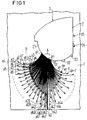
- the layer waveguide 2 with the diffraction grating 3, a plurality of coupling-in waveguides 40, a multiplicity of coupling-out waveguides al to an and a multiplicity of optical detectors d1 to dn are integrated on the substrate 1.
- a plurality of coupling-in waveguides 40, a multiplicity of coupling-out waveguides al to an and a multiplicity of optical detectors d1 to dn are integrated on the substrate 1.
- Figure 2 section A lead ten adjacent current input waveguide 40 to a respective coupling point 10 on the edge 21 of the slab waveguide 2.
- the coupling-in waveguide 40 in the form of ridge waveguides and the Auskoppelwellenleiter are for example performed al up in the form of strip waveguides .
- Each coupling waveguide leads from a coupling point p1 to pn assigned to it to an optical detector d1 to dn assigned to it.
- the wavelength channels ⁇ 1 to ⁇ n to be demultiplexed are coupled into a coupling waveguide 40 and guided to the associated coupling point 10, in which they are coupled into the layer waveguide 2.
- the wavelength channels ⁇ 1 to ⁇ n are guided to a diffraction grating which is formed on a section of the edge 21 of the layered waveguide 2.
- the grid 3 is preferred a focusing grating, in which the relevant section of the edge 21 runs along a curved line in a sawtooth shape, as is not shown to scale and exaggerated in FIG.
- the grating splits the supplied wavelength channels ⁇ 1 to ⁇ n spectrally.
- the channels ⁇ 1 to ⁇ n spectrally decomposed are guided by the layer waveguide 2 in the direction of the coupling-out waveguides al up to the edge 21 of the layer waveguide 2.
- the focusing grating 3 has the effect that each wavelength channel is focused on an associated decoupling point on the edge of the layer waveguide 21.
- the outcoupling waveguide coupled to this outcoupling point acts like an exit slit in a spectrograph and corresponds to a wavelength channel.
- the width of the coupling waveguide or the distance between the coupling waveguides determine the channel width or the channel spacing.
- Each coupling-out waveguide feeds the wavelength channel coupled into it to the optical detector to which it is connected.
- the optical detector detects this channel.
- a method for producing the exemplary embodiment according to FIG. 1 is described below by way of example: A layer package is applied to a substrate 1 made of InP, which consists of a buffer layer 101 made of InP applied directly on the substrate 1 but not always necessary, of a wave-guiding layer 102 made of InGaAsP on the buffer layer 101, and a cover layer 103 made of InP on the wave-guiding layer Layer 102, an absorption layer 104 made of InGaAs on the cover layer 103 and a contact layer 105 made of InP on the absorption layer 104.
- a passivation layer for example made of SiN x, is applied to the contact layer 105 and can be produced by means of a CVD process.
- a local doping 109 is carried out, which in the case of n-doped substrate 1 is p-doping and p-doped substrate 1 is n-doping. This doping can take place by means of diffusion or ion implantation.
- This first structural level can be omitted if the contact layer 105 is already produced in the epitaxy in a doped manner. This leads to a simpler structure, but also to stability problems of the photodiode, since the pn junction at the heterojunction is exposed on the flank of the mesa-shaped raised region 119 produced in this method.
- the doped contact layer 105 is contacted in the local areas.
- contact pads 108 made of TiPtAu are structured, which are produced, for example, by means of known lifting technology and contact the contact layer 105 through an opening 116 in the passivation layer 106.
- the mesa-shaped raised regions 119 are produced by etching down to the top layer 103.
- This etching can be done for example by reactive ion etching (RIE), for example with CH mit / H2.
- RIE reactive ion etching
- the layer waveguide 2, the grating 3 and the input and output waveguides 40 and al are defined up to now with the aid of a mask layer 107.
- This mask layer 107 can be a passivation layer that remains on the arrangement.
- the mask layer 107 can consist of SiN x , which is applied by means of a CVD process.
- the structure of the mask layer 107 is shown in a top view in FIG.
- the mask layer 107 of the coupling-in waveguide 40 is first covered in a fifth structure level with a second mask layer, not shown, which also covers regions of the cover layer 103 lying laterally of the mask layer 107.
- This second mask layer can consist of photoresist, for example.
- etching is carried out to a depth below the waveguiding layer 102.
- RIE with CH4 / H2 is also suitable for this etching.
- the coupling-in waveguides 40 are etched as etched waveguides by etching the exposed lateral areas of the cover layer 103. This can also be done using RIE with CH4 / H2. In this step, the other waveguide 2 and Al to An and the diffraction grating 3 are etched deeper.
- the etched end faces of the diffraction grating 3 are vapor-deposited with metal in order to increase the diffraction efficiency of the grating. This can be done using known lifting technology.
- the layer package is dimensioned such that it can be produced together with the photodiode in an epitaxy.
- the gap wavelength of the material of the waveguiding layer which is 1.05 ⁇ m, keeps the polarization dispersion low.
- the buffer layer 101 has a thickness of more than 2 ⁇ m.
- the waveguiding layer 102 has a gap wavelength of 1.05 ⁇ m and a thickness of 0.5 ⁇ m.
- the thickness of the cover layer 103 is 0.2 ⁇ m.
- the thickness of the absorption layer is 1 ⁇ m and the thickness of the contact layer is 0.5 ⁇ m. All these Layers are applied in an epitaxial step.
- the substrate 1 made of InP can be n-doped or semi-insulating in order to achieve better HF properties.
- n-doping is carried out in the lower half of the buffer layer 101 in order to enable a low-resistance connection of the n-region of the photodiodes. Additional structural steps are also required to define the n-type contact and pull the p-type contacts out onto the semi-insulating substrate.
- the version with the n-doped substrate 1 is technologically simpler.
- the width of the single-mode coupling waveguide 40 is chosen at a rib height of 0.2 ⁇ m so that the light emerges at the coupling point 10 with the largest possible divergence angle of, for example, ⁇ 10 ° in order to illuminate as many grating teeth as possible, which means high resolution.
- the spectrum at the photodiodes d1 to dn can be shifted and a desired central wavelength can be placed on a photodiode by selecting a suitable coupling-in waveguide 40.
- the curved diffraction grating 3 is dimensioned in such a way that, given the resolution of the lithography method, the greatest possible dispersion in the smallest possible order of the arrangement is possible.
- the section of the edge 21 of the layer waveguide 2, on which the coupling points p1 to pn lie, is an arc that corresponds to the Rowland circle.
- the distance between the coupling-out waveguides is chosen to be about 10 ⁇ m for a channel distance of 4 nm.
- the width of the coupling waveguide is chosen as large as possible at 9 ⁇ m.
- the coupling-out waveguides a1 to an are guided on circular arcs with a radius of more than 1 mm until the spacing of these waveguides is so great that bond pads with an area of 50x100 ⁇ m2 have space on the photodiodes. If a semi-insulating substrate is used, the photodiodes can be made narrower because the bond pads are no longer on the photodiode itself. In this case, the required distance of the coupling-out waveguides from one another results from the routing of the conductor tracks from the p-contacts to the bond pads and their position on the substrate.
- the pads can be wired using wedge bonding.
- the photodiodes d1 to dn are arranged in three rows one behind the other in order to save space and at the same time to ensure the greatest possible distance between the pads, by means of which electrical crosstalk is suppressed.
- the minimum resolvable grating period is 1.6 ⁇ m. With this resolution, a dispersion of 1 mrad / nm in the fourth order of the arrangement is made possible.
- the light which is diffracted by the fourth order diffraction grating 3 into the zeroth, first, second or third order is also focused in the vicinity of the Rowland circle. This light can be detected in photodiodes D1 to D5.
- These photodiodes D1 to D5 can be produced like the photodiodes d1 to dn and receive a reference signal which corresponds to the sum of the channels received.
- the intensity of the signals provides information about the diffraction efficiency of the grating 3 in the individual orders.
- the width of the photodiodes d1 to dn is determined by the size of the bond pad when it lies on the diode itself. Otherwise they have a minimum width of about 15 ⁇ m.
- the polarization dispersion can be reduced to approximately 0.7 nm by a thicker cover layer 103 with a thickness of approximately 1 ⁇ m. A further reduction in the dispersion is achieved by subsequently coating this top layer with metal to achieve (see German patent application P 39 31 705.6).
- the above-mentioned example of the production process is modified in such a way that a separate layer package for the waveguides 2, a1, .. is used in a double epitaxy. a n , 40 and a separate layer package for the photodiodes (d1 to dn) are grown.
- the buffer layer 101, the wave-guiding layer 102, and the cover layer 103 are grown on the substrate with a thickness of 1 ⁇ m.
- this cover layer 103 is masked wherever only the waveguides 2, al to an , 40 are to be created. Then, by means of selective etching, for example in HCL, the thick cover layer 103 made of InP is removed everywhere else up to the waveguiding layer 102 made of InGaAsP.
- the layer package for the photodiodes is then selectively grown on the exposed waveguiding layer 102.
- This layer package consists of an absorption layer 104 made of InGaAs with a thickness of 1 ⁇ m and a contact layer 105 made of InP with a thickness of 0.5 ⁇ m.
- the two epitaxial steps can also be carried out in reverse order, depending on which order proves to be technologically more favorable.
- the horizontal structuring is carried out as in the manufacturing example given first, starting with the first structural level.
- the spectral range of an arrangement produced by the above production examples is 1.3 ⁇ m to 1.6 ⁇ m. With a channel spacing of 4 nm, up to 100 channels are available.
- the monolithic integration of demultiplexer and photodiodes eliminates the need for complex and sensitive adjustments in this arrangement, which is therefore suitable as a receiver module for DWDM systems.
- the arrangement according to the invention shown schematically in FIG. 7 is suitable for bidirectional operation and differs from the arrangement according to FIG. 1 essentially by one or more additional optical transmitters 8, only one transmitter 8 being shown for the sake of simplicity.
- the arrangement according to FIG. 7 can be used for a bidirectional subsystem at the subscriber.
- the arrangement transmits at one or more wavelengths and receives and demultiplexes a plurality of wavelength channels, the transmission and reception wavelengths being relatively far apart.
- the transmitters 8 transmit at a wavelength ⁇ 0 in a range at 1.5 ⁇ m and the receiver in the range from 1.28 ⁇ m to 1.38 ⁇ m at a channel spacing ⁇ ⁇ of 4 nm.
- the light supplied by the receiver via a line fiber 9 is guided from the coupling-in waveguide 40 designed as an optical amplifier 4 to the coupling-in point 10 on the edge 21 of the layered waveguide 2 and coupled into the layered waveguide 2 at the coupling-in point 10.
- the light propagates laterally with an aperture angle according to the width of the coupling-in waveguide 40 in the direction r and strikes the diffraction grating 3, from which the light is focused on the coupling-out points p1 to pn.
- the coupling-on waveguides a1 which are freely coupled to the layer waveguide at the decoupling points p1 to pn, lead to photodiodes d1 to dn up to the various wavelength channels ⁇ 1 to ⁇ n .
- These photodiodes d1 to dn are expediently made of InGaAsp with a gate wavelength of about 1.4 ⁇ m, so that the light of the wavelength channels is in the range from 1.28 to 1.38 ⁇ m is absorbed, the light of the optical transmitter 8 is transmitted in the wavelength range at 1.5 ⁇ m, however, and is therefore not converted into a photocurrent.
- the diffraction grating is in a Littrow arrangement with a Littrow wavelength with respect to the optical transmitter 8, which is preferably designed in the form of a semiconductor laser.
- the semiconductor lasers of the respective transmission channel are designed with an active layer for an emission wavelength of approximately 1.53 ⁇ m.
- the optical resonators are delimited on one side by an end face or an etched mirror and on the other side by the grating, which represents a partially reflecting mirror for light of the transmission wavelength.
- Another order of the diffraction grating 3 focuses the light of the transmission wavelength in the direction re to the coupling point 10, where this light is coupled into the coupling waveguide 40.
- a plurality of lasers 8 can be arranged side by side, similarly to the coupling-in waveguides 40 according to FIG. 1, so that the emission wavelength of a laser is in any case at the Littrow wavelength of the diffraction grating 3.
- the coupling-in waveguide 40 is designed as an optical amplifier 4 for the wavelength range around 1.3 ⁇ m.
- the end face 41 of the coupling-in waveguide 4 is also anti-reflective for the wavelength range 1.28 to 1.38 ⁇ m in order to increase the detection sensitivity.
- the efficiency of the laser can be increased if the anti-reflective layer on this end face 41 acts as a reflective coating of 1.53 ⁇ m.
- Such an end face coating consists, for example, of two differently refractive layers of different thickness.
- the grating is dimensioned as follows: the grating period is 1.5 ⁇ m, the angle ⁇ L between the emission direction r0 and the grating normal 31 is 52.36 ° in the fifth diffraction order (no gloss angle).
- the fourth order for the light of the wavelength 1.53 ⁇ m is then emitted by the grating 3 in a direction re to the coupling point 10, which inserts an angle ⁇ i of 28.36 ° with the grating normal 31. This means almost glossy angles.
- the light of the wavelength 1.3 ⁇ m coupled into the layer waveguide 2 at the coupling point 10 strikes the grating 3 in a direction r, which includes the same angle ⁇ i of 28.36 ° with the grating normal 31.
- This light is emitted in a fifth order in a main direction to the decoupling points p1 to pn, which includes an angle ⁇ a of 60.54 ° with the grating normal 31 (glancing angle).
- the light with a wavelength of 1.3 ⁇ m is emitted in fourth order at an angle of approximately 37 ° with a significantly lower diffraction efficiency (no glancing angle).
- the grating is given a gloss or blaze angle, so that the coupling of light of the wavelength of 1.3 ⁇ m from the coupling-in waveguide 40 into the photodiode d1 to dn is optimized.
- the surface of the lattice teeth generating the gloss is set down at an angle of 44.45 ° to the lattice normal 31.
Landscapes
- Physics & Mathematics (AREA)
- General Physics & Mathematics (AREA)
- Optics & Photonics (AREA)
- Engineering & Computer Science (AREA)
- Microelectronics & Electronic Packaging (AREA)
- Condensed Matter Physics & Semiconductors (AREA)
- Electromagnetism (AREA)
- Optical Integrated Circuits (AREA)
- Optical Communication System (AREA)
- Optical Couplings Of Light Guides (AREA)
Applications Claiming Priority (4)
| Application Number | Priority Date | Filing Date | Title |
|---|---|---|---|
| DE4103095 | 1991-02-01 | ||
| DE4103095 | 1991-02-01 | ||
| DE4105465 | 1991-02-21 | ||
| DE4105465 | 1991-02-21 |
Publications (2)
| Publication Number | Publication Date |
|---|---|
| EP0497358A1 true EP0497358A1 (fr) | 1992-08-05 |
| EP0497358B1 EP0497358B1 (fr) | 1996-04-24 |
Family
ID=25900707
Family Applications (1)
| Application Number | Title | Priority Date | Filing Date |
|---|---|---|---|
| EP92101575A Expired - Lifetime EP0497358B1 (fr) | 1991-02-01 | 1992-01-30 | Dispositif optique intégré pour démultiplexage de plusieurs canaux de longueurs d'onde différents et méthode de sa fabrication |
Country Status (4)
| Country | Link |
|---|---|
| US (1) | US5206920A (fr) |
| EP (1) | EP0497358B1 (fr) |
| JP (1) | JPH04344601A (fr) |
| DE (1) | DE59206072D1 (fr) |
Cited By (9)
| Publication number | Priority date | Publication date | Assignee | Title |
|---|---|---|---|---|
| EP0568236A2 (fr) * | 1992-04-29 | 1993-11-03 | AT&T Corp. | Multiplexeurs et démultiplexeurs optiques réflectifs efficaces |
| EP0590331A2 (fr) * | 1992-09-01 | 1994-04-06 | Fuji Xerox Co., Ltd. | Réseau de communication optique |
| EP0672924A1 (fr) * | 1994-03-16 | 1995-09-20 | Fujitsu Limited | Dispositif de commutation optique |
| US5684899A (en) * | 1992-03-05 | 1997-11-04 | Fuji Xerox Co., Ltd. | Optical communication network |
| EP1754330A1 (fr) * | 2004-06-04 | 2007-02-21 | Enablence, Inc. | Transmetteur/récepteur optique bidirectionnel à deux étages |
| EP2062076A1 (fr) * | 2006-10-11 | 2009-05-27 | Huawei Technologies Co., Ltd. | Procédé et système destinés à des points de prise de réseau, visant à surveiller une antenne réseau émettrice dwdm intégrée à une plateforme de circuit d'ondes lumineuses planes (plc) |
| US8285149B2 (en) | 2006-10-02 | 2012-10-09 | Futurewei Technologies, Inc. | Method and system for integrated DWDM transmitters |
| US8285151B2 (en) | 2006-10-20 | 2012-10-09 | Futurewei Technologies, Inc. | Method and system for hybrid integrated 1XN DWDM transmitter |
| US8285150B2 (en) | 2006-10-02 | 2012-10-09 | Futurewei Technologies, Inc. | Method and system for integrated DWDM transmitters |
Families Citing this family (44)
| Publication number | Priority date | Publication date | Assignee | Title |
|---|---|---|---|---|
| US5351262A (en) * | 1992-09-10 | 1994-09-27 | Bell Communications Research, Inc. | Multi-stripe array grating integrated cavity laser |
| US5305412A (en) * | 1992-12-14 | 1994-04-19 | Xerox Corporation | Semiconductor diode optical switching arrays utilizing low-loss, passive waveguides |
| US5475780A (en) * | 1993-06-17 | 1995-12-12 | At&T Corp. | Optical waveguiding component comprising a band-pass filter |
| US5917625A (en) * | 1993-09-09 | 1999-06-29 | Kabushiki Kaisha Toshiba | High resolution optical multiplexing and demultiplexing device in optical communication system |
| US5764821A (en) * | 1994-02-06 | 1998-06-09 | Lucent Technologies Inc. | Large capacity local access network |
| US5457760A (en) * | 1994-05-06 | 1995-10-10 | At&T Ipm Corp. | Wavelength division optical multiplexing elements |
| US5838470A (en) * | 1995-07-27 | 1998-11-17 | University Technology Corporation | Optical wavelength tracking receiver |
| FR2742882B1 (fr) * | 1995-12-22 | 1998-02-13 | Corning Inc | Demultiplexeur de longueurs d'onde, realise en optique integree |
| EP0816877A1 (fr) * | 1996-07-01 | 1998-01-07 | Corning Incorporated | Multiplexeur/démultiplexeur avec réponse spectrale aplatie |
| US5745616A (en) * | 1996-11-27 | 1998-04-28 | Lucent Technologies Inc. | Waveguide grating router and method of making same having relatively small dimensions |
| US6303934B1 (en) * | 1997-04-10 | 2001-10-16 | James T. Daly | Monolithic infrared spectrometer apparatus and methods |
| US6169838B1 (en) * | 1998-04-17 | 2001-01-02 | Jian-Jun He | Athermal waveguide grating based device having a temperature compensator in the slab waveguide region |
| US5937113A (en) * | 1998-04-17 | 1999-08-10 | National Research Council Of Canada | Optical grating-based device having a slab waveguide polarization compensating region |
| FR2779535B1 (fr) * | 1998-06-04 | 2000-09-01 | Instruments Sa | Multiplexeur compact |
| US6137930A (en) * | 1998-07-08 | 2000-10-24 | Optical Switch Corporation | Method and apparatus for aligning optical fibers |
| US6236787B1 (en) | 1998-07-08 | 2001-05-22 | Optical Switch Corporation | Method and apparatus for aligning optical fibers using an alignment spacer |
| US6253007B1 (en) | 1998-07-08 | 2001-06-26 | Optical Switch Corporation | Method and apparatus for connecting optical fibers |
| US6236778B1 (en) | 1998-12-16 | 2001-05-22 | Optical Switch Corporation | Frustrated total internal reflection bus and method of operation |
| US6445479B1 (en) | 1998-12-18 | 2002-09-03 | Lsi Logic Corporation | Electronically controlled optically-active device array for high-speed receiving and transmitting of fiber optic signals |
| US6243511B1 (en) | 1999-02-04 | 2001-06-05 | Optical Switch Corporation | System and method for determining the condition of an optical signal |
| US6304692B1 (en) | 1999-09-03 | 2001-10-16 | Zolo Technologies, Inc. | Echelle grating dense wavelength division multiplexer/demultiplexer with two dimensional single channel array |
| US7167615B1 (en) | 1999-11-05 | 2007-01-23 | Board Of Regents, The University Of Texas System | Resonant waveguide-grating filters and sensors and methods for making and using same |
| US6947220B1 (en) | 1999-11-22 | 2005-09-20 | Ksm Associates, Inc. | Devices for information processing in optical communications |
| US6795605B1 (en) * | 2000-08-01 | 2004-09-21 | Cheetah Omni, Llc | Micromechanical optical switch |
| US6411424B1 (en) * | 2000-09-18 | 2002-06-25 | Intel Corporation | Integrated laser array devices |
| US7050723B2 (en) * | 2001-01-19 | 2006-05-23 | Nippon Telegraph And Telephone Corporation | Laser oscillator, optical communication method and system |
| US7145704B1 (en) | 2003-11-25 | 2006-12-05 | Cheetah Omni, Llc | Optical logic gate based optical router |
| WO2002063361A1 (fr) * | 2001-02-07 | 2002-08-15 | Digilens Inc | Dispositif optique de multiplexage/demultiplexage |
| US6594409B2 (en) * | 2001-04-18 | 2003-07-15 | Apic Corporation | WDM transmitter or receiver including an array waveguide grating and active optical elements |
| US6792182B1 (en) * | 2001-08-28 | 2004-09-14 | Metrophotonics, Inc. | Optical cross connect device with single grating |
| US7209611B2 (en) * | 2002-10-08 | 2007-04-24 | Infinera Corporation | Transmitter photonic integrated circuit (TxPIC) chips utilizing compact wavelength selective combiners/decombiners |
| US7116851B2 (en) * | 2001-10-09 | 2006-10-03 | Infinera Corporation | Optical signal receiver, an associated photonic integrated circuit (RxPIC), and method improving performance |
| EP1436870A2 (fr) * | 2001-10-09 | 2004-07-14 | Infinera Corporation | Circuits integres photoniques d'emetteurs (txpic) et reseaux de transport optique utilisant lesdits txpic |
| US6542671B1 (en) | 2001-12-12 | 2003-04-01 | Super Light Wave Corp. | Integrated 3-dimensional multi-layer thin-film optical couplers and attenuators |
| US7006719B2 (en) * | 2002-03-08 | 2006-02-28 | Infinera Corporation | In-wafer testing of integrated optical components in photonic integrated circuits (PICs) |
| US7747114B2 (en) * | 2002-10-08 | 2010-06-29 | Infinera Corporation | Tilted combiners/decombiners and photonic integrated circuits (PICs) employing the same |
| AU2003287709A1 (en) * | 2002-11-13 | 2004-06-03 | Battelle Memorial Institute | Optical wavelength division mux/demux with integrated optical amplifier |
| KR100679241B1 (ko) * | 2004-12-14 | 2007-02-05 | 한국전자통신연구원 | 광 편향기를 구비한 파장가변 다중화기, 역다중화기 및 파장가변 레이저 |
| DE102007020138B4 (de) * | 2007-04-28 | 2014-06-12 | Esa Patentverwertungsagentur Sachsen-Anhalt Gmbh | Optische Frequenzweiche für die Übertragung von optischen Signalen mit unterschiedlicher Wellenlänge |
| US7974504B2 (en) * | 2008-03-28 | 2011-07-05 | Infinera Corporation | Reflection suppression in a photonic integrated circuit |
| CA2728330C (fr) * | 2008-06-17 | 2016-08-09 | Enablence Inc. | Structure de guide d'ondes segmente |
| US8278741B2 (en) * | 2009-06-30 | 2012-10-02 | Intel Corporation | Sidewall photodetector |
| US9134479B2 (en) * | 2012-09-05 | 2015-09-15 | International Business Machines Corporation | Polarization diverse demultiplexing |
| WO2015157351A1 (fr) * | 2014-04-09 | 2015-10-15 | Robin Huang | Systèmes laser combinant des faisceaux de longueur d'onde intégrés |
Citations (3)
| Publication number | Priority date | Publication date | Assignee | Title |
|---|---|---|---|---|
| EP0275795A1 (fr) * | 1986-12-31 | 1988-07-27 | Commissariat A L'energie Atomique | Multiplexeur-démultiplexeur utilisant un réseau concave elliptique et réalisé en optique intégrée |
| EP0356190A2 (fr) * | 1988-08-26 | 1990-02-28 | AT&T Corp. | Procédé de fabrication pour circuits intégrés photoniques |
| EP0383138A2 (fr) * | 1989-02-16 | 1990-08-22 | Siemens Aktiengesellschaft | Dispositif pour la réception optique directe d'une pluralité de longueurs d'ondes |
Family Cites Families (9)
| Publication number | Priority date | Publication date | Assignee | Title |
|---|---|---|---|---|
| US4696536A (en) * | 1985-07-01 | 1987-09-29 | The United States Of America As Represented By The Secretary Of The Navy | Integrated optical wavelength demultiplexer |
| US4776661A (en) * | 1985-11-25 | 1988-10-11 | Canon Kabushiki Kaisha | Integrated optical device |
| DE3687162D1 (de) * | 1985-12-10 | 1993-01-07 | Siemens Ag | Integriert-optischer multiplex-demultiplex-modul fuer die optische nachrichtenuebertragung. |
| US4715027A (en) * | 1986-05-29 | 1987-12-22 | Polaroid Corporation | Integrated optic multi/demultiplexer |
| EP0560412A3 (en) * | 1987-03-16 | 1993-12-08 | Siemens Ag | Arrangement of optical-integrated spectrometer and method for making the same |
| EP0393372A3 (fr) * | 1989-04-21 | 1991-10-16 | Siemens Aktiengesellschaft | Méthode de fabrication d'un réseau de diffraction formé sur un guide d'onde optique plan |
| US5077822A (en) * | 1989-09-22 | 1991-12-31 | Siemens Aktiengesellschaft | Optical film or strip waveguide having a dielectric waveguiding layer |
| DE4004445A1 (de) * | 1990-02-14 | 1991-08-22 | Schenck Ag Carl | Ankerwiderstandsmessung an reihenschluss-gleichstrommaschinen |
| US5136671A (en) * | 1991-08-21 | 1992-08-04 | At&T Bell Laboratories | Optical switch, multiplexer, and demultiplexer |
-
1992
- 1992-01-23 US US07/824,354 patent/US5206920A/en not_active Expired - Fee Related
- 1992-01-29 JP JP4040399A patent/JPH04344601A/ja not_active Withdrawn
- 1992-01-30 EP EP92101575A patent/EP0497358B1/fr not_active Expired - Lifetime
- 1992-01-30 DE DE59206072T patent/DE59206072D1/de not_active Expired - Fee Related
Patent Citations (3)
| Publication number | Priority date | Publication date | Assignee | Title |
|---|---|---|---|---|
| EP0275795A1 (fr) * | 1986-12-31 | 1988-07-27 | Commissariat A L'energie Atomique | Multiplexeur-démultiplexeur utilisant un réseau concave elliptique et réalisé en optique intégrée |
| EP0356190A2 (fr) * | 1988-08-26 | 1990-02-28 | AT&T Corp. | Procédé de fabrication pour circuits intégrés photoniques |
| EP0383138A2 (fr) * | 1989-02-16 | 1990-08-22 | Siemens Aktiengesellschaft | Dispositif pour la réception optique directe d'une pluralité de longueurs d'ondes |
Non-Patent Citations (2)
| Title |
|---|
| APPLIED PHYSICS LETTERS. Bd. 59, Nr. 6, 5. August 1991, NEW YORK US Seiten 627 - 629; CREMER ET AL.: 'Grating spectrograph in InGaAsP/InP for dense wavelength division multiplexing' * |
| ITG-FACHBERICHTE, KONFERENZ üBER HETEROSTRUKTUR-BAUELEMENTE Bd. 112, 27. April 1990, SCHWäBISCH GMüND, DE Seiten 125 - 130; CREMER: 'Integriert optischer Spektrograph für WDM Komponenten' * |
Cited By (17)
| Publication number | Priority date | Publication date | Assignee | Title |
|---|---|---|---|---|
| US5915054A (en) * | 1992-03-05 | 1999-06-22 | Fuji Xerox Co., Ltd. | Star coupler for an optical communication network |
| US5684899A (en) * | 1992-03-05 | 1997-11-04 | Fuji Xerox Co., Ltd. | Optical communication network |
| US5854700A (en) * | 1992-03-05 | 1998-12-29 | Fuji Xerox Co., Ltd. | Optical communication network |
| EP0568236B1 (fr) * | 1992-04-29 | 1999-06-16 | AT&T Corp. | Multiplexeurs et démultiplexeurs optiques réflectifs efficaces |
| EP0568236A2 (fr) * | 1992-04-29 | 1993-11-03 | AT&T Corp. | Multiplexeurs et démultiplexeurs optiques réflectifs efficaces |
| EP0590331A2 (fr) * | 1992-09-01 | 1994-04-06 | Fuji Xerox Co., Ltd. | Réseau de communication optique |
| EP0590331A3 (en) * | 1992-09-01 | 1994-09-14 | Fuji Xerox Co Ltd | Optical communication network |
| US5477363A (en) * | 1994-03-16 | 1995-12-19 | Fujitsu Limited | Optical switching device |
| EP0672924A1 (fr) * | 1994-03-16 | 1995-09-20 | Fujitsu Limited | Dispositif de commutation optique |
| EP1754330A1 (fr) * | 2004-06-04 | 2007-02-21 | Enablence, Inc. | Transmetteur/récepteur optique bidirectionnel à deux étages |
| EP1754330A4 (fr) * | 2004-06-04 | 2010-12-22 | Enablence Inc | Transmetteur/récepteur optique bidirectionnel à deux étages |
| US8285149B2 (en) | 2006-10-02 | 2012-10-09 | Futurewei Technologies, Inc. | Method and system for integrated DWDM transmitters |
| US8285150B2 (en) | 2006-10-02 | 2012-10-09 | Futurewei Technologies, Inc. | Method and system for integrated DWDM transmitters |
| EP2062076A1 (fr) * | 2006-10-11 | 2009-05-27 | Huawei Technologies Co., Ltd. | Procédé et système destinés à des points de prise de réseau, visant à surveiller une antenne réseau émettrice dwdm intégrée à une plateforme de circuit d'ondes lumineuses planes (plc) |
| EP2062076A4 (fr) * | 2006-10-11 | 2009-09-09 | Huawei Tech Co Ltd | Procédé et système destinés à des points de prise de réseau, visant à surveiller une antenne réseau émettrice dwdm intégrée à une plateforme de circuit d'ondes lumineuses planes (plc) |
| US8050525B2 (en) | 2006-10-11 | 2011-11-01 | Futurewei Technologies, Inc. | Method and system for grating taps for monitoring a DWDM transmitter array integrated on a PLC platform |
| US8285151B2 (en) | 2006-10-20 | 2012-10-09 | Futurewei Technologies, Inc. | Method and system for hybrid integrated 1XN DWDM transmitter |
Also Published As
| Publication number | Publication date |
|---|---|
| DE59206072D1 (de) | 1996-05-30 |
| US5206920A (en) | 1993-04-27 |
| JPH04344601A (ja) | 1992-12-01 |
| EP0497358B1 (fr) | 1996-04-24 |
Similar Documents
| Publication | Publication Date | Title |
|---|---|---|
| EP0497358B1 (fr) | Dispositif optique intégré pour démultiplexage de plusieurs canaux de longueurs d'onde différents et méthode de sa fabrication | |
| EP0187198B1 (fr) | Procédé pour la fabrication d'une structure optique intégrée | |
| EP0284910B1 (fr) | Dispositif optique intégré pour transmission bidirectionnelle de signaux de communications optiques | |
| DE60026367T2 (de) | Integrierter opto-elektronischer wellenlängenwandler | |
| DE19617921C2 (de) | Integrierter optischer Modul mit Wellenleiter und Fotoempfangsvorrichtung | |
| DE60118035T2 (de) | Resonanzreflektor zur verwendung mit optoelektronischen einrichtungen | |
| DE69637437T2 (de) | In InP/InGaAs monolithisch integrierter Demultiplexer, PI Heteroübergang-Bipolartransistor | |
| EP0187979B1 (fr) | Module WDM-demultiplex intégré monolithique et procédé de sa fabrication | |
| DE69534989T2 (de) | Integriertes optisches Regelelement und Verfahren zu seiner Herstellung und integriertoptisches Element und es verwendende integriertoptische Schaltkreisanordnung | |
| DE102015219056B4 (de) | Halbleiterlichtquelle und Verfahren zur Herstellung einer Halbleiterlichtquelle | |
| DE60012704T2 (de) | Abstimmbarer laser mit einer integrierten vorrichtung zur wellenlängenüberwachung und zugehöriges betriebsverfahren | |
| WO1998011461A1 (fr) | Systeme pour interconnecter des guides d'ondes | |
| DE10136727A1 (de) | Photonische Halbleitervorrichtung und Verfahren zu ihrer Herstellung | |
| WO1996017417A1 (fr) | Groupement emetteur-recepteur pour systeme duplex optique | |
| DE10201126A1 (de) | Optoelektronisches Bauelement und Verfahren zu seiner Herstellung | |
| DE60105956T2 (de) | Halbleiterphotodetektor und sein Herstellungsverfahren | |
| DE60128212T2 (de) | Verfahren und Vorrichtung zur Wellenformung eines optischen Signals | |
| DE3329719A1 (de) | Fotodiode mit resonatorstruktur zur absorptionserhoehung | |
| DE60204702T2 (de) | Verbesserungen für optische vorrichtungen | |
| EP1145063B1 (fr) | Composant electro-optique a canaux multiples | |
| EP0442312A2 (fr) | Emetteur et/ou récepteur optique intégré | |
| EP0826256B1 (fr) | Procede de production d'une diode laser a reaction distribuee (dfb) a guide d'ondes accouple et structure de couches d'une diode laser a reaction distribuee | |
| EP1384101B1 (fr) | Systeme pour multiplexer et/ou demultiplexer les signaux d'au moins deux canaux de longueurs d'onde optiques | |
| DE3609278A1 (de) | Integrierte optische halbleiteranordnung | |
| WO1999043055A1 (fr) | Composant pourvu d'un emetteur de lumiere et d'un recepteur de lumiere |
Legal Events
| Date | Code | Title | Description |
|---|---|---|---|
| PUAI | Public reference made under article 153(3) epc to a published international application that has entered the european phase |
Free format text: ORIGINAL CODE: 0009012 |
|
| AK | Designated contracting states |
Kind code of ref document: A1 Designated state(s): DE FR GB |
|
| 17P | Request for examination filed |
Effective date: 19921216 |
|
| 17Q | First examination report despatched |
Effective date: 19950104 |
|
| GRAH | Despatch of communication of intention to grant a patent |
Free format text: ORIGINAL CODE: EPIDOS IGRA |
|
| GRAA | (expected) grant |
Free format text: ORIGINAL CODE: 0009210 |
|
| AK | Designated contracting states |
Kind code of ref document: B1 Designated state(s): DE FR GB |
|
| REF | Corresponds to: |
Ref document number: 59206072 Country of ref document: DE Date of ref document: 19960530 |
|
| ET | Fr: translation filed | ||
| GBT | Gb: translation of ep patent filed (gb section 77(6)(a)/1977) |
Effective date: 19960715 |
|
| PG25 | Lapsed in a contracting state [announced via postgrant information from national office to epo] |
Ref country code: GB Effective date: 19970130 |
|
| PLBE | No opposition filed within time limit |
Free format text: ORIGINAL CODE: 0009261 |
|
| STAA | Information on the status of an ep patent application or granted ep patent |
Free format text: STATUS: NO OPPOSITION FILED WITHIN TIME LIMIT |
|
| 26N | No opposition filed | ||
| GBPC | Gb: european patent ceased through non-payment of renewal fee |
Effective date: 19970130 |
|
| PG25 | Lapsed in a contracting state [announced via postgrant information from national office to epo] |
Ref country code: FR Effective date: 19970930 |
|
| PG25 | Lapsed in a contracting state [announced via postgrant information from national office to epo] |
Ref country code: DE Effective date: 19971001 |
|
| REG | Reference to a national code |
Ref country code: FR Ref legal event code: ST |