EP0568236A2 - Multiplexeurs et démultiplexeurs optiques réflectifs efficaces - Google Patents
Multiplexeurs et démultiplexeurs optiques réflectifs efficaces Download PDFInfo
- Publication number
- EP0568236A2 EP0568236A2 EP93303021A EP93303021A EP0568236A2 EP 0568236 A2 EP0568236 A2 EP 0568236A2 EP 93303021 A EP93303021 A EP 93303021A EP 93303021 A EP93303021 A EP 93303021A EP 0568236 A2 EP0568236 A2 EP 0568236A2
- Authority
- EP
- European Patent Office
- Prior art keywords
- waveguides
- optical
- optical signals
- grating
- signals
- Prior art date
- Legal status (The legal status is an assumption and is not a legal conclusion. Google has not performed a legal analysis and makes no representation as to the accuracy of the status listed.)
- Granted
Links
Images

Classifications
-
- G—PHYSICS
- G02—OPTICS
- G02B—OPTICAL ELEMENTS, SYSTEMS OR APPARATUS
- G02B6/00—Light guides; Structural details of arrangements comprising light guides and other optical elements, e.g. couplings
- G02B6/10—Light guides; Structural details of arrangements comprising light guides and other optical elements, e.g. couplings of the optical waveguide type
- G02B6/12—Light guides; Structural details of arrangements comprising light guides and other optical elements, e.g. couplings of the optical waveguide type of the integrated circuit kind
- G02B6/12007—Light guides; Structural details of arrangements comprising light guides and other optical elements, e.g. couplings of the optical waveguide type of the integrated circuit kind forming wavelength selective elements, e.g. multiplexer, demultiplexer
- G02B6/12009—Light guides; Structural details of arrangements comprising light guides and other optical elements, e.g. couplings of the optical waveguide type of the integrated circuit kind forming wavelength selective elements, e.g. multiplexer, demultiplexer comprising arrayed waveguide grating [AWG] devices, i.e. with a phased array of waveguides
- G02B6/12011—Light guides; Structural details of arrangements comprising light guides and other optical elements, e.g. couplings of the optical waveguide type of the integrated circuit kind forming wavelength selective elements, e.g. multiplexer, demultiplexer comprising arrayed waveguide grating [AWG] devices, i.e. with a phased array of waveguides characterised by the arrayed waveguides, e.g. comprising a filled groove in the array section
-
- G—PHYSICS
- G02—OPTICS
- G02B—OPTICAL ELEMENTS, SYSTEMS OR APPARATUS
- G02B6/00—Light guides; Structural details of arrangements comprising light guides and other optical elements, e.g. couplings
- G02B6/10—Light guides; Structural details of arrangements comprising light guides and other optical elements, e.g. couplings of the optical waveguide type
- G02B6/12—Light guides; Structural details of arrangements comprising light guides and other optical elements, e.g. couplings of the optical waveguide type of the integrated circuit kind
- G02B6/12007—Light guides; Structural details of arrangements comprising light guides and other optical elements, e.g. couplings of the optical waveguide type of the integrated circuit kind forming wavelength selective elements, e.g. multiplexer, demultiplexer
- G02B6/12009—Light guides; Structural details of arrangements comprising light guides and other optical elements, e.g. couplings of the optical waveguide type of the integrated circuit kind forming wavelength selective elements, e.g. multiplexer, demultiplexer comprising arrayed waveguide grating [AWG] devices, i.e. with a phased array of waveguides
- G02B6/12019—Light guides; Structural details of arrangements comprising light guides and other optical elements, e.g. couplings of the optical waveguide type of the integrated circuit kind forming wavelength selective elements, e.g. multiplexer, demultiplexer comprising arrayed waveguide grating [AWG] devices, i.e. with a phased array of waveguides characterised by the optical interconnection to or from the AWG devices, e.g. integration or coupling with lasers or photodiodes
Definitions
- This invention relates to optical multiplexing and demultiplexing. More specifically, this invention relates to reflective optical multiplexing and demultiplexing devices. Those devices comprise small integrated structures which are highly efficient and can handle a large number of communications channels without a large amount of cross-talk between channels.
- Efficient optical multiplexers and demultiplexers suitable for long haul and local area communications networks can be realized in integrated form. See, for example, U.S. Patent 5,002,350.
- These efficient multiplexers and demultiplexers comprise a plurality of essentially uncoupled transmissive waveguides which effectively provide unequal path lengths between a group of input waveguides and a group of output wave guides.
- the unequal length waveguides essentially act as a grating whose order is determined by the difference in path length between the adjacent waveguides.
- the size of multiplexer/demultiplexer devices using such transmissive waveguides to perform the function of an optical grating tends to be large.
- the size of these transmissive devices may, in fact, be too large to be practical, especially when the number of channels handled by the device is large, the required level of crosstalk between channels is very low, and the channel width is small. This large size is due, in part, to the long bends needed in the grating to produce the required path length differences in the grating.
- the spacing between waveguides must be relatively large - for example, more than twice the width of each waveguide - which requires a further increase in the size of the device.
- compositional variations cause variations in the propagation constant of the waveguides. Changes in the propagation constant will cause phase errors in the optical signals flowing in the waveguides. Such phase errors will noticeably increase the cross-talk between channels in a large size multiplexing and demultiplexing device and will seriously reduce the efficiency of the device.
- the size of a multiplexer/demultiplexer device may be reduced by adopting a reflective geometry in place of a transmissive geometry like the prior art geometry described above. High efficiency and low levels of cross-talk achieved by transmissive geometries are maintained. Also, a large number of channels may be multiplexed or demultiplexed by such a small size reflective device.
- a first plurality of waveguides is connected to a free space region.
- the first plurality of waveguides may comprise a group of waveguides which may carry input optical signals interleaved with a group of waveguides which may carry output optical signals.
- a second plurality of waveguides is also connected to the flee space region.
- Each of the second plurality of waveguides is terminated with a reflective element.
- a reflective device can be smaller than a corresponding transmissive device for a given number of channels handled by the device.
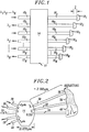
- FIG. 1 is a schematic representation of an integrated multiplexer/demultiplexer in accordance with this invention which uses a reflective optical grating containing waveguides terminated with reflective elements.
- FIG. 2 is a more detailed representation of an example of a reflective multiplexer/demultiplexer in accordance with this invention.
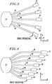
- FIG. 3 shows an example of an optical grating in accordance with this invention comprising straight waveguides terminated in Bragg reflectors.
- FIG. 4 shows an example of an optical grating in accordance with this invention comprising curved waveguides terminated in Bragg reflectors which are located so that they are displaced from one another by only x and y linear displacements.
- FIG. 5 shows a grating waveguide terminated in a reflective element comprising a diffraction grating which has been separately made and then affixed to one end of the grating waveguide.
- FIG. 6 shows a grating waveguide terminated in a reflective element comprising a diffraction grating which has been directly machined into one end of the grating waveguide.
- FIG. 1 shows an optical multiplexer/demultiplexer which comprises a plurality of input ports and a plurality of output ports.
- An optical grating couples the input ports to the output ports and comprises a plurality of waveguides terminated in reflective elements.
- FIG. 1 schematically shows an example of a reflective optical NxN multiplexer/demultiplexer in accordance with this invention.
- the device of FIG. 1 comprises a group of N input waveguides 101, 102,..., and 10 N one or more of which each may carry up to N optical signals which have been multiplexed together by some instrumentality external to the device of FIG. 1.
- N may be up to 20 or more.
- These multiplexed optical signals are directed into the device for demultiplexing via waveguides 101, 102,..., and 10 N , which act as input ports of the device, when the device is used as a demultiplexer for these signals.
- the device demultiplexes the multiplexed optical signals received on each one of the input ports.
- the demultiplexed optical signals are directed out of the device via a second group of N output waveguides 121, 122,..., and 12 N , which act as output ports of the device when waveguides 101, 102,..., and 10 N are used as input ports.
- a plurality of the waveguides 121, 122,..., and 12 N each may carry a single wavelength optical input signal.
- Those single optical input signals are multiplexed by the device of FIG. 1 and directed out of the device on one of the waveguides 101, 102,..., 10 N .
- the waveguides 121, 122,..., and 12 N act as the input ports of the device and waveguides 101, 102,..., and 10 N act as output ports of the device.
- the output waveguides are interleaved with the input waveguides so that every other waveguide connected to the boundary 11 of the free space region 14 is a waveguide for carrying input signals and every other waveguide connected to boundary 11 is a waveguide for carrying output signals.
- N may be up to 20 or more for the output waveguides. Although described as being equal in number here, the number of input waveguides may differ from the number of output waveguides.
- the device of FIG. 1 also comprises a planar free space region 14 connected to the pluralities of waveguides 10 and 12.
- the free space region 14 is also connected to an optical reflective grating comprising M unequal length waveguides 161, 162, 163, 164, 165,..., and 16 M .
- the length of each waveguide in the grating differs from its immediately adjacent neighboring waveguides by a constant predetermined magnitude l, as shown in FIG. 1.
- One end of each of the waveguides 16 in the grating is connected to the free space region 14.
- the other end of each of the waveguides 16 is terminated in reflective elements 181, 182, 183, 184, 185,..., and 18 M , respectively.
- M may be up to 35 or more.
- the device of FIG. 1 may be fabricated from a silicon wafer by forming regions of SiO2 in the wafer defining the configurations of the waveguides and free space region. The formation of such regions may be made by photolithographic patterning techniques.
- the reflective elements 18 may be formed by creating appropriate reflective compositional discontinuities in the waveguides 18 in the grating.
- An alternative material which may be used to form the device of FIG. 1 comprises semiconductor material such as indium phosphide (InP) having regions of a quaternary composition, such as InP doped with gallium arsenide InGaAsP, defining the waveguides and free space region shown in FIG. 1.
- FIG. 1 illustrates one example of the use of the illustrated device as a demultiplexer for input signals in waveguide 101.
- a plurality of optical wavelengths ⁇ 1, ⁇ 2, ... ⁇ N are directed toward the free space region 14 via the waveguide 101.
- the wavelengths ⁇ 1, ⁇ 2, ... ⁇ N travel through the waveguide 101, into the free space region 14, and illuminate the optical grating.
- Some of the energy received from waveguide 101 is directed through each of the waveguides 161, 162..., and 16 M in the grating toward a respective one of the reflective elements 181, 182,..., or 18 M .
- the energy flowing in each of the waveguides 16 is reflected from a respective reflective element back toward the free space region 14.
- each of the waveguides 16 differs in length from its immediately adjacent neighboring waveguide in the optical grating by an amount l, as shown in FIG. 1, there is a corresponding phase shift between the reflected energy directed into the free space region 14 by each of the waveguides 16.
- This phase shift causes each individual optical wavelength in the original multiplexed signal introduced into the device on waveguide 101 to be focused or concentrated on different ones of the waveguides 121, 122,..., and 12 N for carrying demultiplexed optical wavelengths.
- FIG. 1 shows that each of the waveguides 16 differs in length from its immediately adjacent neighboring waveguide in the optical grating by an amount l, as shown in FIG. 1, there is a corresponding phase shift between the reflected energy directed into the free space region 14 by each of the waveguides 16.
- This phase shift causes each individual optical wavelength in the original multiplexed signal introduced into the device on waveguide 101 to be focused or concentrated on different ones of the waveguides 121, 122,..., and 12 N for carrying demultiplexe
- optical energy at wavelength ⁇ 1 is directed out of the device on waveguide 121
- optical energy at wavelength ⁇ 2 is directed out of the device on waveguide 122
- so forth up to optical energy at ⁇ N being directed out of the device on waveguide 12 N
- multiplexed optical signals may also be applied simultaneously or separately to the other waveguides 102 to 10 N in addition to waveguide 101. Those signals will be demultiplexed and directed to individual ones of the waveguides 121, 122,..., and 12 N . For example, the same wavelengths ⁇ 1, ⁇ 2,..., and ⁇ N may be directed to any of the other waveguides 102 to 10 N .
- Each individual wavelength will be demultiplexed and will appear as an output on one of the waveguides 121, 122..., and 12 N .
- the waveguide 121, 122,..., and 12 N on which a particular wavelength appears is a function of which waveguide 101, 102,..., or 10 N received that wavelength.
- the device of FIG. 1 may also perform as a multiplexer, since each output waveguide in general may receive signals from all input waveguides.
- each output waveguide in general may receive signals from all input waveguides.
- those input optical wavelengths will be multiplexed by the device and appear in combination at the output of the device on one of the waveguides 101, 102,..., and 10 N .
- the identity of a waveguide at which a desired unmultiplexed or multiplexed optical wavelength appears as an output is determined by the wavelength of an input signal and by which of the input waveguides receives input optical wavelength for demultiplexing or multiplexing.
- FIG. 2 shows a more detailed example of an integrated optical multiplexing/demultiplexing device in accordance with this invention.
- the device of FIG. 2 comprises waveguides and a planar free space region made of InGaAsP regions formed on or in an InP substrate.
- the device of FIG. 2 may be an NxN multiplexer capable of multiplexing and demultiplexing N optical wavelengths, where N may be as large as 16 or more.
- the device of FIG. 2 contains a plurality of waveguides.
- the plurality of waveguides comprises N waveguides for carrying input optical signals. Three of those waveguides for carrying input optical signals are labeled with reference numerals 20, 22, and 24 in FIG. 2.
- the plurality of waveguides also comprises N waveguides for carrying output optical signals. Two of the waveguides for carrying output optical signals are labeled with reference numerals 26 and 28 in FIG. 2.
- the device of FIG. 2 also comprises a free space region 14 connected to one end of each of the waveguides described above.
- the free space region 14 may comprise a flat area having a length D of about 670 ⁇ m.
- the waveguides described above may be about 2 ⁇ m wide.
- the waveguides may be separated by about 1 ⁇ m at the circular boundary of the free space region 14.
- the wavelength channels ⁇ 1, ⁇ 2,..., ⁇ N handled by the device of FIG. 2 may be separated by about 0.8 nanometers. ⁇ 1 may be about 1.5 ⁇ m.
- the device of FIG. 2 contains an optical grating comprising M waveguides, three of which are labeled in FIG. 2 with reference numerals 30, 32, and 34.
- the value of M may be about 35 in one example of the invention.
- the M waveguides in the grating are of unequal length. Specifically, the length of each waveguide in the grating differs from the length of its immediately adjacent waveguides in the grating by a constant length l. More specifically, for the waveguides shown in FIG. 2, the length of waveguide 30 is l units of length longer than the length of waveguide 32. Waveguide 32, in turn, is l units of length longer than waveguide 34.
- the value of l may be about 75 ⁇ m.
- Each of the waveguides in the grating may be separated from its immediate neighbors by an angular separation of about 0.255°.
- the length of the longest waveguide in the optical grating may be about 3300 ⁇ m.
- Each of the waveguides in the grating is terminated with a reflective element as in FIG. 1. Specifically, for the waveguides shown in FIG. 2, waveguide 30 is terminated in a reflective element 36, waveguide 32 is terminated in a reflective element 38, and waveguide 34 is terminated in a reflective element 40.
- the device of FIG. 2 operates in a fashion similar to the device of FIG. 1 to multiplex and demultiplex optical signals directed to selected ones of the waveguides for carrying multiplexed and unmultiplexed signals described above.
- variable phase shifters for example, a modulator using the electroptic effect
- a modulator using the electroptic effect may be located in each of the grating arms to obtain a tunable grating.
- phase errors caused by nonuniformity in the wafer and other phase uberrations can be removed thus reducing cross-talk in the device.
- FIGs. 3 and 4 show two embodiments of the invention using Bragg reflectors as the reflecting elements.
- the Bragg reflectors may be formed in the wafer at the end of each waveguide in the grating by forming a number of closely spaced grooves in the wafer which act as a reflecting grating.
- the advantage of using Bragg reflectors in this manner is that when each Bragg reflector is appropriately situated with respect to the optical energy flowing in its respective waveguide, the losses due to reflection can be very small, for example, less than 1 dB.
- the grating waveguides 42, 44, 46, 48, and 50 are each unequal length straight-line waveguides extending from the free space region 14 to Bragg reflectors 52, 54, 56, 58, and 60, each of which is appropriately oriented with respect to the longitudinal axis of its respective waveguide so that maximum reflection of the incident optical energy occurs.
- the Bragg reflectors shown in FIG. 3 are thus linearly displaced from one another in both the x,y directions in the plane of the wafer and are also rotationally displaced with respect to one another and equally spaced. It may thus be somewhat difficult to fabricate the geometry of FIG. 3 using stepping equipment which must individually form the Bragg reflectors in the wafer.
- FIG. 4 depicts the Bragg reflectors 62, 64, 66, 68, 70, 72, and 74 which are only linearly displaced from one another in the x,y plane without any rotational displacement.
- This arrangement of Bragg reflectors requires that the grating waveguides 76, 78, 80, 82, 84, 86, and 88 terminated by the Bragg reflectors to be somewhat curved, but this curvature is not too severe, the bends in the waveguides are not too long, and little appreciable loss is introduced.
- the edge of the wafer may be directly machined into the form of an optical diffraction grating 92.
- the gratings of FIGs. 5 and 6 are preferably configured so that each facet of the grating is illuminated at normal incidence.
- the depth of each groove should be approximately equal to ⁇ /2.
- the latter condition can only be satisfied exactly at one wavelength.
- This condition can be satisfied by properly chosing the waveguide width which is inversely related to the waveguide angular aperture determined by the far field width of the waveguide mode.
- One or more of the devices disclosed here may be used to multiplex or demultiples optical signals produced by equipment in an optical fiber based long haul or local area communications network, such as a local or long distance public switched telephone network, using entirely or, in part, optical fibers or other optical signal transmitting medium and the like to transmit communications signals from place-to-place in the network.
- Communications systems using optical multiplexers and demultiplexers in accordance with this invention comprise one or more pieces of equipment which produce optical signals for transmission to one or more receivers of the optical signals.
- the multiplexers and demultiplexers of this invention may be part of the communications path between the equipment which produces the optical signals and the equipment which receives those optical signals.
Applications Claiming Priority (2)
| Application Number | Priority Date | Filing Date | Title |
|---|---|---|---|
| US87592792A | 1992-04-29 | 1992-04-29 | |
| US875927 | 1992-04-29 |
Publications (3)
| Publication Number | Publication Date |
|---|---|
| EP0568236A2 true EP0568236A2 (fr) | 1993-11-03 |
| EP0568236A3 EP0568236A3 (en) | 1994-08-17 |
| EP0568236B1 EP0568236B1 (fr) | 1999-06-16 |
Family
ID=25366625
Family Applications (1)
| Application Number | Title | Priority Date | Filing Date |
|---|---|---|---|
| EP93303021A Expired - Lifetime EP0568236B1 (fr) | 1992-04-29 | 1993-04-20 | Multiplexeurs et démultiplexeurs optiques réflectifs efficaces |
Country Status (4)
| Country | Link |
|---|---|
| US (1) | US5450511A (fr) |
| EP (1) | EP0568236B1 (fr) |
| JP (1) | JPH06102430A (fr) |
| DE (1) | DE69325309T2 (fr) |
Cited By (5)
| Publication number | Priority date | Publication date | Assignee | Title |
|---|---|---|---|---|
| EP0653821A2 (fr) * | 1993-11-15 | 1995-05-17 | AT&T Corp. | Laser accordable de façon numérique par réflection |
| FR2743234A1 (fr) * | 1995-12-28 | 1997-07-04 | Alcatel Optronics | Demultiplexeur de longueurs d'onde |
| WO1998039676A1 (fr) * | 1997-03-03 | 1998-09-11 | Akzo Nobel N.V. | Antenne reseau polymere a commande de phase |
| EP0864891A1 (fr) * | 1997-03-03 | 1998-09-16 | Akzo Nobel N.V. | Réseau de phase polymère |
| WO2005081022A1 (fr) * | 2004-02-19 | 2005-09-01 | Keio University | Réseau sélectif planétaire de diffraction |
Families Citing this family (89)
| Publication number | Priority date | Publication date | Assignee | Title |
|---|---|---|---|---|
| US5475780A (en) * | 1993-06-17 | 1995-12-12 | At&T Corp. | Optical waveguiding component comprising a band-pass filter |
| US6236782B1 (en) | 1995-08-29 | 2001-05-22 | Arroyo Optics, Inc. | Grating assisted coupler devices |
| US5875272A (en) * | 1995-10-27 | 1999-02-23 | Arroyo Optics, Inc. | Wavelength selective optical devices |
| JPH11511568A (ja) | 1995-08-29 | 1999-10-05 | アロヨ・オプティクス・インコーポレイテッド | 波長選択回折格子利用型光学カプラ |
| EP0857314A4 (fr) * | 1995-10-27 | 1999-03-24 | Arroyo Optics Inc | Dispositifs optiques selectifs en longueurs d'ondes |
| US6239868B1 (en) | 1996-01-02 | 2001-05-29 | Lj Laboratories, L.L.C. | Apparatus and method for measuring optical characteristics of an object |
| US6254385B1 (en) | 1997-01-02 | 2001-07-03 | Lj Laboratories, Llc | Apparatus and method for measuring optical characteristics of teeth |
| US5966205A (en) | 1997-07-01 | 1999-10-12 | Lj Laboratories, Llc | Method and apparatus for detecting and preventing counterfeiting |
| US6307629B1 (en) | 1997-08-12 | 2001-10-23 | Lj Laboratories, L.L.C. | Apparatus and method for measuring optical characteristics of an object |
| US6373573B1 (en) | 2000-03-13 | 2002-04-16 | Lj Laboratories L.L.C. | Apparatus for measuring optical characteristics of a substrate and pigments applied thereto |
| US5759030A (en) | 1996-01-02 | 1998-06-02 | Lj Laboratories, L.L.C. | Method for determing optical characteristics of teeth |
| US6118521A (en) * | 1996-01-02 | 2000-09-12 | Lj Laboratories, L.L.C. | Apparatus and method for measuring optical characteristics of an object |
| US5880826A (en) | 1997-07-01 | 1999-03-09 | L J Laboratories, L.L.C. | Apparatus and method for measuring optical characteristics of teeth |
| US5768450A (en) * | 1996-01-11 | 1998-06-16 | Corning Incorporated | Wavelength multiplexer/demultiplexer with varied propagation constant |
| US6111674A (en) * | 1996-02-23 | 2000-08-29 | Corning Incorporated | Multiple reflection multiplexer and demultiplexer |
| US6169830B1 (en) | 1996-08-26 | 2001-01-02 | Arroyo Optics, Inc. | Methods of fabricating grating assisted coupler devices |
| EP0879465B1 (fr) * | 1996-11-07 | 2005-11-16 | Koninklijke Philips Electronics N.V. | Traitement informatique d'un signal de train binaire |
| US6233047B1 (en) | 1997-01-02 | 2001-05-15 | Lj Laboratories, L.L.C. | Apparatus and method for measuring optical characteristics of an object |
| US6301004B1 (en) | 2000-05-31 | 2001-10-09 | Lj Laboratories, L.L.C. | Apparatus and method for measuring optical characteristics of an object |
| US5889906A (en) * | 1997-05-28 | 1999-03-30 | Lucent Technologies Inc. | Signal router with coupling of multiple waveguide modes for provicing a shaped multi-channel radiation pattern |
| US6870616B2 (en) | 1998-06-30 | 2005-03-22 | Jjl Technologies Llc | Spectrometer apparatus for determining an optical characteristic of an object or material having one or more sensors for determining a physical position or non-color property |
| US6271913B1 (en) | 1997-07-01 | 2001-08-07 | Lj Laboratories, Llc | Apparatus and method for measuring optical characteristics of an object |
| US6449041B1 (en) | 1997-07-01 | 2002-09-10 | Lj Laboratories, Llc | Apparatus and method for measuring optical characteristics of an object |
| US6501542B2 (en) | 1998-06-30 | 2002-12-31 | Lj Laboratories, Llc | Apparatus and method for measuring optical characteristics of an object |
| IT1295868B1 (it) * | 1997-10-23 | 1999-05-28 | Italtel Spa | De/multiplatore o instradatore in lunghezza d'onda (wdm) |
| US6246471B1 (en) | 1998-06-08 | 2001-06-12 | Lj Laboratories, Llc | Apparatus and method for measuring optical characteristics of an object |
| US6246479B1 (en) | 1998-06-08 | 2001-06-12 | Lj Laboratories, L.L.C. | Integrated spectrometer assembly and methods |
| US6573984B2 (en) | 1998-06-30 | 2003-06-03 | Lj Laboratories Llc | Apparatus and method for measuring optical characteristics of teeth |
| US6249348B1 (en) | 1998-11-23 | 2001-06-19 | Lj Laboratories, L.L.C. | Integrated spectrometer assembly and methods |
| US6538726B2 (en) | 1998-07-10 | 2003-03-25 | Lj Laboratories, Llc | Apparatus and method for measuring optical characteristics of an object |
| US6661942B1 (en) | 1998-07-20 | 2003-12-09 | Trans Photonics, Llc | Multi-functional optical switch (optical wavelength division multiplexer/demultiplexer, add-drop multiplexer and inter-connect device) and its methods of manufacture |
| US6023480A (en) * | 1999-02-02 | 2000-02-08 | Lucent Technologies Inc. | Fast tunable multiwavelength laser with folded imaging arrangement of nonoverlapping focal regions |
| US6324322B1 (en) * | 1999-06-07 | 2001-11-27 | Wavesplitter Technologies, Inc. | Fused-fiber multi-window wavelength filter using unbalanced Michelson Interferometer |
| JP2001166162A (ja) * | 1999-12-09 | 2001-06-22 | Hitachi Cable Ltd | アレイ導波路型グレーティング |
| KR100358177B1 (ko) * | 1999-12-10 | 2002-10-25 | 한국전자통신연구원 | 반사형 다중기/역다중기 및 그 제조방법 |
| US6362888B1 (en) | 1999-12-23 | 2002-03-26 | Lj Laboratories, L.L.C. | Spectrometer assembly |
| US6519037B2 (en) | 1999-12-23 | 2003-02-11 | Lj Laboratories, Llc | Spectrometer having optical unit including a randomized fiber optic implement |
| US6414750B2 (en) | 2000-01-10 | 2002-07-02 | Lj Laboratories, L.L.C. | Spectrometric apparatus and method for measuring optical characteristics of an object |
| USRE42407E1 (en) | 2000-03-16 | 2011-05-31 | Steyphi Services De Llc | Distributed optical structures with improved diffraction efficiency and/or improved optical coupling |
| US6965464B2 (en) * | 2000-03-16 | 2005-11-15 | Lightsmyth Technologies Inc | Optical processor |
| US6987911B2 (en) * | 2000-03-16 | 2006-01-17 | Lightsmyth Technologies, Inc. | Multimode planar waveguide spectral filter |
| US7773842B2 (en) * | 2001-08-27 | 2010-08-10 | Greiner Christoph M | Amplitude and phase control in distributed optical structures |
| USRE41570E1 (en) | 2000-03-16 | 2010-08-24 | Greiner Christoph M | Distributed optical structures in a planar waveguide coupling in-plane and out-of-plane optical signals |
| USRE42206E1 (en) | 2000-03-16 | 2011-03-08 | Steyphi Services De Llc | Multiple wavelength optical source |
| US7519248B2 (en) * | 2000-03-16 | 2009-04-14 | Lightsmyth Technologies Inc | Transmission gratings designed by computed interference between simulated optical signals and fabricated by reduction lithography |
| US7194164B2 (en) * | 2000-03-16 | 2007-03-20 | Lightsmyth Technologies Inc | Distributed optical structures with improved diffraction efficiency and/or improved optical coupling |
| US6879441B1 (en) | 2000-03-16 | 2005-04-12 | Thomas Mossberg | Holographic spectral filter |
| AU2001282849A1 (en) * | 2000-04-28 | 2001-11-20 | Confluent Photonics, Inc. | Miniature monolithic optical devices for dwdm |
| US6553165B1 (en) | 2000-07-14 | 2003-04-22 | Applied Wdm, Inc. | Optical waveguide gratings |
| US6434303B1 (en) | 2000-07-14 | 2002-08-13 | Applied Wdm Inc. | Optical waveguide slab structures |
| US6493487B1 (en) | 2000-07-14 | 2002-12-10 | Applied Wdm, Inc. | Optical waveguide transmission devices |
| AU2002213362A1 (en) * | 2000-10-19 | 2002-04-29 | Trans Photonics, L.L.C. | Novel substituted-polyaryl chromophoric compounds |
| US6596185B2 (en) | 2000-11-28 | 2003-07-22 | Lightcross, Inc. | Formation of optical components on a substrate |
| US6563997B1 (en) | 2000-11-28 | 2003-05-13 | Lighteross, Inc. | Formation of a surface on an optical component |
| US7113704B1 (en) | 2000-11-28 | 2006-09-26 | Kotura, Inc. | Tunable add/drop node for optical network |
| US6574396B1 (en) * | 2001-03-12 | 2003-06-03 | Lucent Technologies Inc. | Waveguide grating arrangement using a segmented reflector |
| US6792180B1 (en) | 2001-03-20 | 2004-09-14 | Kotura, Inc. | Optical component having flat top output |
| US20020158047A1 (en) * | 2001-04-27 | 2002-10-31 | Yiqiong Wang | Formation of an optical component having smooth sidewalls |
| US20020158046A1 (en) * | 2001-04-27 | 2002-10-31 | Chi Wu | Formation of an optical component |
| US6853773B2 (en) * | 2001-04-30 | 2005-02-08 | Kotusa, Inc. | Tunable filter |
| US6614965B2 (en) | 2001-05-11 | 2003-09-02 | Lightcross, Inc. | Efficient coupling of optical fiber to optical component |
| US6674929B2 (en) | 2001-06-01 | 2004-01-06 | Lightcross, Inc. | Tunable optical filter |
| US20020181869A1 (en) * | 2001-06-01 | 2002-12-05 | Wenhua Lin | Tunable dispersion compensator |
| US6571034B2 (en) | 2001-06-28 | 2003-05-27 | Corning Incorporated | Spectrally-shaped optical components using a wavelength-dispersive element and a reflective array |
| US20030012537A1 (en) * | 2001-07-11 | 2003-01-16 | Chi Wu | Method of forming an optical component |
| US6614951B2 (en) | 2001-08-06 | 2003-09-02 | Lightcross, Inc. | Optical component having a flat top output |
| US6853797B2 (en) * | 2001-11-05 | 2005-02-08 | Kotura, Inc. | Compact optical equalizer |
| US20030091291A1 (en) * | 2001-11-15 | 2003-05-15 | Sam Keo | Smoothing facets on an optical component |
| US6714704B2 (en) | 2001-11-29 | 2004-03-30 | Lightcross, Inc. | Optical component having selected bandwidth |
| US6650796B2 (en) * | 2002-02-21 | 2003-11-18 | Northrop Grumman Corporation | Waveguide optical frequency router |
| US6903813B2 (en) | 2002-02-21 | 2005-06-07 | Jjl Technologies Llc | Miniaturized system and method for measuring optical characteristics |
| US6810168B1 (en) | 2002-05-30 | 2004-10-26 | Kotura, Inc. | Tunable add/drop node |
| US6885795B1 (en) | 2002-05-31 | 2005-04-26 | Kotusa, Inc. | Waveguide tap monitor |
| US7224855B2 (en) * | 2002-12-17 | 2007-05-29 | Lightsmyth Technologies Inc. | Optical multiplexing device |
| US7260290B1 (en) | 2003-12-24 | 2007-08-21 | Lightsmyth Technologies Inc | Distributed optical structures exhibiting reduced optical loss |
| US7181103B1 (en) | 2004-02-20 | 2007-02-20 | Lightsmyth Technologies Inc | Optical interconnect structures incorporating sets of diffractive elements |
| US7151635B2 (en) * | 2004-03-24 | 2006-12-19 | Enablence, Inc. | Planar waveguide reflective diffraction grating |
| US7359597B1 (en) | 2004-08-23 | 2008-04-15 | Lightsmyth Technologies Inc | Birefringence control in planar optical waveguides |
| US7120334B1 (en) | 2004-08-25 | 2006-10-10 | Lightsmyth Technologies Inc | Optical resonator formed in a planar optical waveguide with distributed optical structures |
| US7095925B2 (en) * | 2004-11-03 | 2006-08-22 | Intel Corporation | Optical phased array transmitter/receiver |
| US7330614B1 (en) | 2004-12-10 | 2008-02-12 | Lightsmyth Technologies Inc. | Integrated optical spectrometer incorporating sets of diffractive elements |
| US7327908B1 (en) | 2005-03-07 | 2008-02-05 | Lightsmyth Technologies Inc. | Integrated optical sensor incorporating sets of diffractive elements |
| US7349599B1 (en) | 2005-03-14 | 2008-03-25 | Lightsmyth Technologies Inc | Etched surface gratings fabricated using computed interference between simulated optical signals and reduction lithography |
| US7643400B1 (en) | 2005-03-24 | 2010-01-05 | Lightsmyth Technologies Inc | Optical encoding of data with distributed diffractive structures |
| US7190856B1 (en) | 2005-03-28 | 2007-03-13 | Lightsmyth Technologies Inc | Reconfigurable optical add-drop multiplexer incorporating sets of diffractive elements |
| US8068709B2 (en) * | 2005-09-12 | 2011-11-29 | Lightsmyth Technologies Inc. | Transmission gratings designed by computed interference between simulated optical signals and fabricated by reduction lithography |
| WO2013049942A1 (fr) | 2011-10-06 | 2013-04-11 | Valorbec S.E.C. | Réseau de diffraction concave mono-ordre de grande efficacité |
| US8867920B2 (en) | 2012-07-24 | 2014-10-21 | International Business Machines Corporation | Optical de-multiplexing device |
| ES2540378B1 (es) | 2013-12-05 | 2016-05-18 | Univ Politècnica De València | Dispositivo fotonico integrado |
Citations (4)
| Publication number | Priority date | Publication date | Assignee | Title |
|---|---|---|---|---|
| US4087159A (en) * | 1974-09-20 | 1978-05-02 | Max-Planck-Gesellschaft Zur Forderung Der Wissenschaften E.V. | Self imaging system using a waveguide |
| EP0250824A1 (fr) * | 1986-05-29 | 1988-01-07 | Polaroid Corporation | Multi-démultiplexeur optique intégré |
| US5002350A (en) * | 1990-02-26 | 1991-03-26 | At&T Bell Laboratories | Optical multiplexer/demultiplexer |
| EP0497358A1 (fr) * | 1991-02-01 | 1992-08-05 | Siemens Aktiengesellschaft | Dispositif optique intégré pour démultiplexage de plusieurs canaux de longueurs d'onde différents et méthode de sa fabrication |
Family Cites Families (9)
| Publication number | Priority date | Publication date | Assignee | Title |
|---|---|---|---|---|
| US3600594A (en) * | 1968-12-09 | 1971-08-17 | Lockheed Aircraft Corp | Fiber optics pulse width modulator |
| NL8304311A (nl) * | 1983-12-15 | 1985-07-01 | Philips Nv | Reflectieraster. |
| US4886333A (en) * | 1985-08-06 | 1989-12-12 | Hicks John W | Fiber laser sensor |
| US4940306A (en) * | 1988-01-28 | 1990-07-10 | Mitsubishi Denki Kabushiki Kaisha | Star network optical transmission system |
| US4904042A (en) * | 1988-05-03 | 1990-02-27 | American Telephone And Telegraph Company | N×N optical star coupler |
| US4923271A (en) * | 1989-03-28 | 1990-05-08 | American Telephone And Telegraph Company | Optical multiplexer/demultiplexer using focusing Bragg reflectors |
| JPH03263003A (ja) * | 1990-03-14 | 1991-11-22 | Fujitsu Ltd | 光フィルタ |
| US5136600A (en) * | 1990-09-18 | 1992-08-04 | Litton Systems Inc. | Stabilization apparatus and method for an sfs |
| US5142660A (en) * | 1991-03-07 | 1992-08-25 | Litton Systems, Inc. | Broadband light source using rare earth doped glass waveguide |
-
1993
- 1993-04-20 DE DE69325309T patent/DE69325309T2/de not_active Expired - Lifetime
- 1993-04-20 EP EP93303021A patent/EP0568236B1/fr not_active Expired - Lifetime
- 1993-04-28 JP JP5101638A patent/JPH06102430A/ja active Pending
-
1994
- 1994-07-25 US US08/279,982 patent/US5450511A/en not_active Expired - Lifetime
Patent Citations (4)
| Publication number | Priority date | Publication date | Assignee | Title |
|---|---|---|---|---|
| US4087159A (en) * | 1974-09-20 | 1978-05-02 | Max-Planck-Gesellschaft Zur Forderung Der Wissenschaften E.V. | Self imaging system using a waveguide |
| EP0250824A1 (fr) * | 1986-05-29 | 1988-01-07 | Polaroid Corporation | Multi-démultiplexeur optique intégré |
| US5002350A (en) * | 1990-02-26 | 1991-03-26 | At&T Bell Laboratories | Optical multiplexer/demultiplexer |
| EP0497358A1 (fr) * | 1991-02-01 | 1992-08-05 | Siemens Aktiengesellschaft | Dispositif optique intégré pour démultiplexage de plusieurs canaux de longueurs d'onde différents et méthode de sa fabrication |
Non-Patent Citations (3)
| Title |
|---|
| ELECTRONICS LETTERS., vol.24, no.7, 31 March 1988, ENAGE GB pages 385 - 386 SMIT M.K. 'NEW FOCUSING AND DISPERSIVE PLANAR COMPONENT BASED ON OPTICAL PHASED ARRAY' * |
| ELECTRONICS LETTERS., vol.28, no.4, 13 February 1992, ENAGE GB pages 380 - 382 TAKAHASHI H. ET AL. '10GHZ SPACING OPTICAL FREQUENCY DIVISION MULTIPLEXER BASED ON ARRAYED-WAVEGUIDE GRATING' * |
| OPTICS AND LASER TECHNOLOGY, vol. 22, no. 2, April 1990, HAYWARDS HEATH GB, pages 113 - 126 SENIOR J.M. ET AL. 'WAVELENGTH DIVISION MULTIPLEXING IN OPTICAL FIBRE SENSOR SYSTEMS AND NETWORKS: A REVIEW' * |
Cited By (8)
| Publication number | Priority date | Publication date | Assignee | Title |
|---|---|---|---|---|
| EP0653821A2 (fr) * | 1993-11-15 | 1995-05-17 | AT&T Corp. | Laser accordable de façon numérique par réflection |
| EP0653821A3 (fr) * | 1993-11-15 | 1995-08-23 | At & T Corp | Laser accordable de façon numérique par réflection. |
| FR2743234A1 (fr) * | 1995-12-28 | 1997-07-04 | Alcatel Optronics | Demultiplexeur de longueurs d'onde |
| EP0783118A1 (fr) * | 1995-12-28 | 1997-07-09 | Alcatel | Démultiplexeur en longueur d'onde |
| US5751872A (en) * | 1995-12-28 | 1998-05-12 | Alcatel Alsthom Compagnie Generale D'electricite | Wavelength demultiplexer |
| WO1998039676A1 (fr) * | 1997-03-03 | 1998-09-11 | Akzo Nobel N.V. | Antenne reseau polymere a commande de phase |
| EP0864891A1 (fr) * | 1997-03-03 | 1998-09-16 | Akzo Nobel N.V. | Réseau de phase polymère |
| WO2005081022A1 (fr) * | 2004-02-19 | 2005-09-01 | Keio University | Réseau sélectif planétaire de diffraction |
Also Published As
| Publication number | Publication date |
|---|---|
| US5450511A (en) | 1995-09-12 |
| EP0568236A3 (en) | 1994-08-17 |
| DE69325309T2 (de) | 2000-01-27 |
| EP0568236B1 (fr) | 1999-06-16 |
| JPH06102430A (ja) | 1994-04-15 |
| DE69325309D1 (de) | 1999-07-22 |
Similar Documents
| Publication | Publication Date | Title |
|---|---|---|
| EP0568236B1 (fr) | Multiplexeurs et démultiplexeurs optiques réflectifs efficaces | |
| EP0922973B1 (fr) | Multiplexeur/Démultiplexeur optique compensé en température | |
| US5982518A (en) | Optical add-drop multiplexers compatible with very dense WDM optical communication systems | |
| EP0528652B1 (fr) | Multiplexeur et démultiplexeur optique amélioré | |
| US5748349A (en) | Gratings-based optical add-drop multiplexers for WDM optical communication system | |
| US6366378B1 (en) | Optical multiplexing and demultiplexing | |
| US6181849B1 (en) | Interleaved wavelengths multi/demultiplexer with multiple-input-ports and multiple-output-ports for wavelength add/drop WDM systems | |
| EP1225461B1 (fr) | Multiplexeur et démultiplexeur bidirectionnels basés sur un seul réseau de guides d'onde en échelle | |
| EP0613263A1 (fr) | Réseau optique comportant un démultiplexeur de longueur d'onde compact | |
| US5940555A (en) | Optical multiplexer/demultiplexer | |
| EP0649040B1 (fr) | Filtre optique à bande passante | |
| US6512864B1 (en) | Optical multiplexer/demultiplexer arrangement for WDM signals having in-band and out-of-band signal components | |
| US6549313B1 (en) | Broadbrand electronic N×N cross-connect switch using tunable lasers | |
| US6381052B1 (en) | Multiplexors with a flat top spectral channel shape | |
| US6956987B2 (en) | Planar lightwave wavelength blocker devices using micromachines | |
| GB2139374A (en) | Optical multiplexer/demultiplexer | |
| US20020131685A1 (en) | Multiple band optical multiplexer and demultiplexer | |
| US20020081062A1 (en) | Optical grating based multi-input demultiplexer for multiple sets of interleaved wavelength channels | |
| US6347165B1 (en) | Wavelength demultiplexer without waveguide bending loss | |
| WO1999008143A1 (fr) | Multiplexeur optique en longueur d'onde | |
| US20090263084A1 (en) | Arrayed waveguide grating circuit | |
| US7327912B2 (en) | Wavelength division multiplexer/demultiplexer | |
| CN1179510C (zh) | 用于交换光波长的方法和波长选择开关 | |
| US7457497B2 (en) | Optical multiplexer/demultiplexer and optical communication system | |
| US6546167B1 (en) | Tunable grating optical device |
Legal Events
| Date | Code | Title | Description |
|---|---|---|---|
| PUAI | Public reference made under article 153(3) epc to a published international application that has entered the european phase |
Free format text: ORIGINAL CODE: 0009012 |
|
| AK | Designated contracting states |
Kind code of ref document: A2 Designated state(s): DE FR GB NL |
|
| RAP3 | Party data changed (applicant data changed or rights of an application transferred) |
Owner name: AT&T CORP. |
|
| PUAL | Search report despatched |
Free format text: ORIGINAL CODE: 0009013 |
|
| AK | Designated contracting states |
Kind code of ref document: A3 Designated state(s): DE FR GB NL |
|
| 17P | Request for examination filed |
Effective date: 19950202 |
|
| 17Q | First examination report despatched |
Effective date: 19971014 |
|
| GRAG | Despatch of communication of intention to grant |
Free format text: ORIGINAL CODE: EPIDOS AGRA |
|
| GRAG | Despatch of communication of intention to grant |
Free format text: ORIGINAL CODE: EPIDOS AGRA |
|
| GRAG | Despatch of communication of intention to grant |
Free format text: ORIGINAL CODE: EPIDOS AGRA |
|
| GRAH | Despatch of communication of intention to grant a patent |
Free format text: ORIGINAL CODE: EPIDOS IGRA |
|
| GRAH | Despatch of communication of intention to grant a patent |
Free format text: ORIGINAL CODE: EPIDOS IGRA |
|
| GRAA | (expected) grant |
Free format text: ORIGINAL CODE: 0009210 |
|
| AK | Designated contracting states |
Kind code of ref document: B1 Designated state(s): DE FR GB NL |
|
| REF | Corresponds to: |
Ref document number: 69325309 Country of ref document: DE Date of ref document: 19990722 |
|
| ET | Fr: translation filed | ||
| PLBE | No opposition filed within time limit |
Free format text: ORIGINAL CODE: 0009261 |
|
| STAA | Information on the status of an ep patent application or granted ep patent |
Free format text: STATUS: NO OPPOSITION FILED WITHIN TIME LIMIT |
|
| 26N | No opposition filed | ||
| PGFP | Annual fee paid to national office [announced via postgrant information from national office to epo] |
Ref country code: FR Payment date: 20010322 Year of fee payment: 9 |
|
| PGFP | Annual fee paid to national office [announced via postgrant information from national office to epo] |
Ref country code: NL Payment date: 20010327 Year of fee payment: 9 |
|
| REG | Reference to a national code |
Ref country code: GB Ref legal event code: IF02 |
|
| PG25 | Lapsed in a contracting state [announced via postgrant information from national office to epo] |
Ref country code: NL Free format text: LAPSE BECAUSE OF NON-PAYMENT OF DUE FEES Effective date: 20021101 |
|
| PG25 | Lapsed in a contracting state [announced via postgrant information from national office to epo] |
Ref country code: FR Free format text: LAPSE BECAUSE OF NON-PAYMENT OF DUE FEES Effective date: 20021231 |
|
| NLV4 | Nl: lapsed or anulled due to non-payment of the annual fee |
Effective date: 20021101 |
|
| REG | Reference to a national code |
Ref country code: FR Ref legal event code: ST |
|
| PGFP | Annual fee paid to national office [announced via postgrant information from national office to epo] |
Ref country code: DE Payment date: 20120425 Year of fee payment: 20 |
|
| PGFP | Annual fee paid to national office [announced via postgrant information from national office to epo] |
Ref country code: GB Payment date: 20120418 Year of fee payment: 20 |
|
| REG | Reference to a national code |
Ref country code: DE Ref legal event code: R071 Ref document number: 69325309 Country of ref document: DE |
|
| REG | Reference to a national code |
Ref country code: GB Ref legal event code: PE20 Expiry date: 20130419 |
|
| PG25 | Lapsed in a contracting state [announced via postgrant information from national office to epo] |
Ref country code: GB Free format text: LAPSE BECAUSE OF EXPIRATION OF PROTECTION Effective date: 20130419 Ref country code: DE Free format text: LAPSE BECAUSE OF EXPIRATION OF PROTECTION Effective date: 20130423 |