EP0487680B1 - Karte mit integrierter schaltung und elektronische anordnung zu ihrer nutzung - Google Patents
Karte mit integrierter schaltung und elektronische anordnung zu ihrer nutzung Download PDFInfo
- Publication number
- EP0487680B1 EP0487680B1 EP91911268A EP91911268A EP0487680B1 EP 0487680 B1 EP0487680 B1 EP 0487680B1 EP 91911268 A EP91911268 A EP 91911268A EP 91911268 A EP91911268 A EP 91911268A EP 0487680 B1 EP0487680 B1 EP 0487680B1
- Authority
- EP
- European Patent Office
- Prior art keywords
- card
- shutter
- receptacle
- electronic apparatus
- integrated circuit
- Prior art date
- Legal status (The legal status is an assumption and is not a legal conclusion. Google has not performed a legal analysis and makes no representation as to the accuracy of the status listed.)
- Expired - Lifetime
Links
Images


Classifications
-
- G—PHYSICS
- G06—COMPUTING; CALCULATING OR COUNTING
- G06K—GRAPHICAL DATA READING; PRESENTATION OF DATA; RECORD CARRIERS; HANDLING RECORD CARRIERS
- G06K19/00—Record carriers for use with machines and with at least a part designed to carry digital markings
- G06K19/06—Record carriers for use with machines and with at least a part designed to carry digital markings characterised by the kind of the digital marking, e.g. shape, nature, code
-
- H—ELECTRICITY
- H05—ELECTRIC TECHNIQUES NOT OTHERWISE PROVIDED FOR
- H05K—PRINTED CIRCUITS; CASINGS OR CONSTRUCTIONAL DETAILS OF ELECTRIC APPARATUS; MANUFACTURE OF ASSEMBLAGES OF ELECTRICAL COMPONENTS
- H05K5/00—Casings, cabinets or drawers for electric apparatus
- H05K5/02—Details
- H05K5/0256—Details of interchangeable modules or receptacles therefor, e.g. cartridge mechanisms
- H05K5/0286—Receptacles therefor, e.g. card slots, module sockets, card groundings
Definitions
- the present invention relates to a removable integrated circuit card that is inserted into electronic apparatus in order to connect with integrated circuit elements within the card.
- An integrated circuit card encloses one or more integrated circuit elements mounted on a substrate and connected to an electrical contact pattern toward one end of the card.
- a shutter is provided to cover and protect the contact pattern when the card is removed from an electrical connector in the electronic apparatus and to expose the contact pattern for electrical connection when the card is inserted into the connector.
- the connector includes a pair of opening pins that enter holes in a forward area of the card, thereby contacting the shutter and urging the shutter open.
- the pins (and the holes therewith) may be unsymmetrically positioned with respect to the card to prevent wrong-way insertion.
- shutter-opening ridges formed in the connector are keyed to grooves in the card to prevent a wrong-way insertion.
- the card must be fully, or almost fully, inserted before wrong-way insertion can be detected because the shutter opening pins or the grooves act upon the forward-most area of the card.
- This is a problem with respect to a typical situation because the user, upon encountering some reluctance toward the end of a card's travel, might be inclined to jam the card further into the apparatus.
- This is of particular concern since a wrong-way obstruction might easily be mistaken for the force that must be overcome in order to initiate travel of the shutter. It is consequently desirable to provide a wrong-way warning earlier in the card's travel so that there is no mistaking its meaning.
- the invention stems from the recognition that by activating the shutter from the rear end thereof, rather than at its front surface, as is conventional, a single member in the card-receiving apparatus could perform the dual function of preventing wrong-way insertion and opening the shutter. To separate wrong-way detection from the opening function, however, it remains necessary that the functions be temporally separated as the card is inserted, that is, wrong-way detection has to come shortly after the card is inserted and well before shutter travel commences.
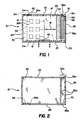
- an integrated circuit card 10 embodying the features of the invention is shown for storing and/or processing data in one or more integrated circuit elements 12.
- a substrate 14 (shown particularly in Figure 3) supports the circuit elements 12 and provides electrical connection(s) 16 (Figure 1) between the elements 12 and a contact area 18 on one end of the substrate 14.
- the contact area 18 is composed of a pattern of individually accessible contacts 18a, 18b, 18c, etc. formed on the surface of the substrate 14.
- a card frame 20 supports the substrate 14, and the circuit elements 12 therewith.
- the frame 20 includes parallel side walls 22 and 24, a front wall 26 on a forward section of the card 10, and a rear wall 28 on a rearward section of the card 10.
- the side walls 22 and 24 are stepped on the interiorly-facing sides thereof, as shown particularly in Figure 3, in order to separately support the substrate 14 in relation to an upper cover 30 and a lower cover 32.
- the upper cover 30 is dimensioned to stop rearwardly of the front of the substrate 14, thus leaving an open portion for exposing the contact pattern 18 to the electronic apparatus.
- the frame 20 includes a recessed chamfer slot 33 having an inclined surface joining the side wall 24 and the front wall 26.
- An elongated opening recess 34 is located toward the rear wall 28 in the side wall 24.
- the recess 34 includes an inclined ramp 34a leading into the recess opening at the forward end thereof.
- the opposite side ( Figure 2) of the frame 20 has forward section 20a with a locking slot 36 formed therein.
- the locking slot 36 has a slightly depressed cross-section such that the floor of the slot is surrounded by slightly projecting walls 36a, particularly on the forward and rearward sides thereof.
- a shutter 38 is supported in the frame 20 between the upper cover 30 and the substrate 14.
- the shutter has a forward surface 38a for covering the contact pattern 18 and a distal surface 38b extending adjacent the opening recess 34.
- a tab 40 extends from the distal surface 38b of the shutter into the opening recess 34.
- the opening recess 34 and the tab 40 therewith are situated along the lateral wall 24 rearwardly of the forward surface 38a of the shutter 38.
- the opening recess 34 and the tab 40 are also situated rearwardly of the chamfer slot 33 on a common side 24 therewith.
- the shutter 38 has a lug 42 extending from each side thereof into respective cavities 44 (Fig. 4) in each side wall 22 and 24.
- a spring 46 is attached between the lug 42 and a post 48 extending from the side wall 22 (or 24).
- the shutter 38 is thus supported for movement within the frame 20 such that the springs 46 tension the shutter 38 forwardly as shown in Figure 1 toward a closed position in which the forward surface 38a covers the contact pattern 18 on the substrate 14.
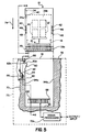
- the card 10 is shown in Figures 5 and 6 in relation to a card-receiving receptacle 70 formed in electronic apparatus 72.
- the electronic apparatus 72 is shown in broken line to include an exemplary electronic circuit, such as a signal processing circuit 72a. The particular processing function is, however, unimportant to an understanding of the invention.
- the card 10 is adapted for manually directed movement as indicated by an arrow 74 (with its opposite side (Fig. 2) upward as shown in Figure 5) through an access opening 76 in a side wall 78 of the electronic apparatus 72.
- the receptacle 70 includes a edge opening 80 containing a lever 82 that is tensioned by a spring 84 to pivot about an axis 86 into the receptacle 70.
- the spring 84 urges an upper extension 82a of the lever 82 against a ledge 88 such that an operative member 90 extending from the lever 82 protrudes into the receptacle 70 for engaging the card.
- the operative member 90 is preferably a boss having a flat surface 90a directly opposed to the entering card 10).
- the receptacle 70 includes side walls 92a and 92b, and edge walls 94a and 94b, that serve to define an enclosed space and to guide the card 10 into the enclosed space of the receptacle.
- the receptacle space is further defined by an end wall 96 situated opposite the access opening 76 in the side wall 78 of the electronic apparatus 72.
- An opening 98 in the side wall 92b situated toward the end wall 96 supports a plurality of electrodes 100 for engaging the contact area 18 of the card 10.
- the electrodes 100 are connected to the signal processing section 72a for transferring electrical information to and/or from the circuit elements 12 on the card 10.
- a further opening 102 is situated in the side wall 92a in generally opposed relation to the electrodes 100 such that a member (schematically shown by an arrow 104) may enter the receptacle 70 to secure the card 10 and force the contact pattern 18 of the card 10 against the electrodes 100.
- the card 10 is initially verified for a correct orientation when first inserted into the receptacle 70. This is shown in Figures 7 and 8 for correct and incorrect (wrong-way) insertion, respectively. If the card 10 is correctly inserted (Fig. 7), the recessed chamfer 33 encounters the operative member 90 and ramps the lever 82 counter-clockwise back into the opening 80. The way is then clear for the card 10 to be further inserted into the receptacle 70. If the card 10 is incorrectly inserted (Fig. 8), the front wall 26 of the card 10 collides with the flat surface 90a of the operative member 90 and further insertion is prevented.
- the card 10 may be fully inserted into the receptacle 70, as shown in Figure 9.
- the now-retracted operative member 90 slides along the side wall 24 of the card 10 until it reaches the opening recess 34.
- the member 90 slides along the ramp surface 34a and into the opening recess 34 and engages the tab 40 depending from the rear surface of the shutter 38. Further movement of the card 10 into the receptacle 70 urges the shutter 38 rearward against the tension of the springs 46 until the front surface 38a retreats sufficiently to expose the contact area 18.
- the card 10 slides across the opening 98 in the side wall 92b of the receptacle and the electrodes 100 make electrical contact with the contact area 18 on the card 10.
- the electrodes 100 are omitted in Fig. 9 in order to keep the illustration clear.
- the schematically-shown member 104 enters the locking slot 36 on the card 10 and secures the card 10 in the receptacle 70 (against the bias of the springs 46 in the card 10) with the contact pattern 18 firmly against the electrodes 100.
- Electrical signals can then be transferred in a conventional manner between the circuit elements 12 on the card 10 and circuits in the electronic apparatus 72, such as the signal processing circuit 72a.
- a principal benefit of an integrated circuit card as described herein is that a single member, the operative member 90, can be used to detect a correct insertion and to open the shutter. This tends to simplify the electronic apparatus 72 and minimize the number of parts. More importantly, one-way insertion can be temporally separated from the shutter opening, that is, correct insertion is detected (Fig. 7) well before the shutter is opened (Fig. 9). This is of significant importance in many applications, such as with consumer products, where the user of the equipment 72 may not exert due care or otherwise mistake the force associated with opening the shutter with the blockage exhibited by wrong-way insertion.
- Manual removal of the card 10 is obtained by basically doing the reverse of the preceding operation.
- the schematically-shown locking member 104 is withdrawn from the locking slot 36 and the card 10 begins to eject under urging of the springs 46 against the operative member 90.
- the rear end of the card 10 is then pulled outward by the user.
- the lever 82 pivots counter clockwise as the inclined ramp 34a of the opening recess 36 ramps the operative member 90 away from the card 10.
- the springs 46 urge the shutter 38 to its closed position where the forward surface 38a overlies and protects the contact area 18.
- the lever 82 pivots clockwise until the upper area thereof meets the ledge 88 and the card-engaging operative member 90 is thrust into the enclosed space of the receptacle opening.
Landscapes
- Engineering & Computer Science (AREA)
- Microelectronics & Electronic Packaging (AREA)
- Physics & Mathematics (AREA)
- General Physics & Mathematics (AREA)
- Theoretical Computer Science (AREA)
- Coupling Device And Connection With Printed Circuit (AREA)
- Details Of Connecting Devices For Male And Female Coupling (AREA)
- Manipulator (AREA)
- Rehabilitation Tools (AREA)
- Conveying Record Carriers (AREA)
- Credit Cards Or The Like (AREA)
Claims (11)
- Elektronisches System mit einer IC-Karte (10) und einem elektronischen Gerät, in dem die Karte in ein Fach (70) einführbar ist, wobei die Karte- Schaltungsmittel (14) mit einem oder mehreren integrierten Schalungselementen (12) und einem Kontaktmuster (18) zum Verbinden der Schaltungselemente (12) mit dem elektronischen Gerät aufweist;- Umschließungsmittel (20, 30, 32) umfaßt, welche die Schaltungsmittel (14) im wesentlichen umhüllen und einen geöffneten Abschnitt aufweisen, durch den das Kontaktmuster (18) für das elektronische Gerät zugänglich ist, wobei der geöffnete Abschnitt im vorderen Bereich der Umschließungsmittel angeordnet ist, der bei korrektem Einschub als erster in das Gerätefach (70) einführbar ist;- eine durch die Umschließungsmittel (20, 30, 32) zur Bewegung relativ zu den Schaltungsmitteln (14) gehaltene Abdeckung (38) aufweist, die ein abstehendes Element (40) zum Bewegen der Abdeckung (38) in eine Offenstellung umfaßt, wobei die Abdeckung (38) üblicherweise in Richtung einer Schließstellung vorgespannt ist, in der ein vorderer Bereich (38a) das Kontaktmuster (18) bedeckt; und- richtungsorientierte Einschubmittel (33) zur Sicherstellung eines ordnungsgemäßen Einschubs der IC-Karte (10) in das Gerätefach (70) aufweist, wobei das Gerät- in das Gerätefach (70) ragende Funktionsmittel (90), aufweist, welche die Karte (10) erfassen und mit den richtungsorientierten Einschubmitteln (33) der Karte (10) zusammenwirken, wobei die Funktionsmittel (90) einen korrekten Einschub sicherstellen, ehe sie mit dem abstehenden Element (40) der Abdeckung zusammenwirken;dadurch qekennzeichnet, daß- das abstehende Element der Abdeckung ein an der distalen Fläche (38b) angebrachter Vorsprung (40) ist, der sich hinter dem vorderen Bereich (38a) befindet und in die Funktionsmittel (90) eingreift, um zusammen mit diesen die Abdeckung (38) in eine Offenstellung zu bewegen, in der das Kontaktmuster (18) für das elektronische Gerät durch den geöffneten Abschnitt zugänglich ist:- die richtungsorientierten Einschubmittel einen ausgesparten, abgeschrägten Schlitz (33) mit einer an den Umschließungsmitteln (20, 30, 32) vor dem Vorsprung (40) angeordneten geneigten Fläche aufweisen, die mit den Funktionsmitteln (90) zusammenwirkt; und- die Funktionsmittel (90) einen zurückziehbaren Hebel (82) aufweisen, der sich in einer Kantenöffnung (80) des Gerätefachs (70) befindet, von einer Feder (84) gespannt wird und um eine Achse (86) ins Innere des Gerätefachs (70) einschwenkt.
- System nach Anspruch 1, dadurch gekennzeichnet, daß sich der abgeschrägte Schlitz (33) an einer vorderen Ecke der Umschließungsmittel befindet.
- System nach Anspruch 1 oder 2, dadurch gekennzeichnet, daß die Umschließungsmittel (20, 30, 32) eine ausgesparte Öffnung (34) aufweisen, damit die in das Gerätefach (70) ragenden Funktionsmittel (90) den Vorsprung (40) erfassen können.
- System nach Anspruch 3, dadurch gekennzeichnet, daß der abgeschrägte Schlitz (33) und die ausgesparte öffnung (34) an einer gemeinsamen Kante (24) der Umschließungsmittel (20, 30, 32) relativ zueinander angeordnet sind, wobei beim Einführen der Karte (10) in das Gerätefach (70) die Funktionsmittel (90) den abgeschrägten Schlitz (33) vor der ausgesparten Öffnung (34) erfassen.
- System nach Anspruch 4, dadurch gekennzeichnet, daß der zurückziehbare Hebel (82) in das Gerätefach (70) ragt, um den Vorsprung (40) zu erfassen, wenn sich die ausgesparte Öffnung (34) an den Funktionsmitteln (90) vorbeibewegt.
- System nach den Ansprüchen 1 - 5, dadurch gekennzeichnet, daß die geneigte Fläche des abgeschrägten Schlitzes (33) den den Hebel erfassenden Hebel (82) aus dem Gerätefach (70) schiebt, wenn die Karte (10) ordnungsgemäß in das Gerätefach (70) eingeführt ist.
- System nach Anspruch 5, dadurch gekennzeichnet, daß bei wiederholter Einführung der Karte der Hebel (82) so angeordnet ist, daß er in die ausgesparte Öffnung (34) eintaucht und den von der Abdeckung (38) abstehenden Vorsprung (40) erfaßt.
- System nach Anspruch 1, dadurch gekennzeichnet, daß die Abdeckung (38) üblicherweise durch mindestens eine zwischen Abdeckung (38) und Umschließungsmittel (20, 30, 32) angeordnete Feder (46) vorgespannt ist.
- System nach einem der vorhergehenden Ansprüche, dadurch gekennzeichnet, daß das elektronische Gerät eine Signalverarbeitungsschaltung (72a) und mit dieser verbundene Elektrodenanschlüsse (100) zum Übertragen von Information zwischen der Signalverarbeitungsschaltung (72a) und der entnehmbaren IC-Karte (10) umfaßt, welche ein oder mehrere, mit dem Kontaktmuster verbundene Speicherelemente (12) aufweist, und daß das Gerätefach (70) die Karte (10) in einem umschlossenen Raum aufnimmt, der durch im wesentlichen parallele Seitenwände (94a, 94b) gebildet ist, welche die Karte (10) in das Gerätefach (70) einführen, wobei die Funktionsmittel (90) von einer der Seitenwände (94a) aus in den umschlossenen Raum ragen.
- System nach Anspruch 9, dadurch gekennzeichnet, daß durch die ausgesparte Öffnung (34) der Hebel (82) in den umschlossenen Raum wiedereintauchen kann, um den von der Abdeckung abstehenden Vorsprung (40) zu erfassen, nachdem er durch die geneigte Fläche abgedrängt wurde.
- System nach Anspruch 10, dadurch gekennzeichnet, daß der Hebel (82) eine Nase (90a) aufweist, die den abstehenden Vorsprung (40) erfaßt und die Abdeckung (38) in ihre Offenstellung bewegt.
Applications Claiming Priority (3)
| Application Number | Priority Date | Filing Date | Title |
|---|---|---|---|
| US07/539,660 US5036430A (en) | 1990-06-18 | 1990-06-18 | Integrated circuit card and electronic apparatus for use therewith |
| US539660 | 1990-06-18 | ||
| PCT/US1991/004040 WO1991020052A1 (en) | 1990-06-18 | 1991-06-10 | Integrated circuit card and electronic apparatus for use therewith |
Publications (2)
| Publication Number | Publication Date |
|---|---|
| EP0487680A1 EP0487680A1 (de) | 1992-06-03 |
| EP0487680B1 true EP0487680B1 (de) | 1996-09-18 |
Family
ID=24152137
Family Applications (1)
| Application Number | Title | Priority Date | Filing Date |
|---|---|---|---|
| EP91911268A Expired - Lifetime EP0487680B1 (de) | 1990-06-18 | 1991-06-10 | Karte mit integrierter schaltung und elektronische anordnung zu ihrer nutzung |
Country Status (8)
| Country | Link |
|---|---|
| US (1) | US5036430A (de) |
| EP (1) | EP0487680B1 (de) |
| JP (1) | JPH05501325A (de) |
| KR (1) | KR920702522A (de) |
| BR (1) | BR9105794A (de) |
| CA (1) | CA2063831C (de) |
| DE (1) | DE69122215T2 (de) |
| WO (1) | WO1991020052A1 (de) |
Families Citing this family (44)
| Publication number | Priority date | Publication date | Assignee | Title |
|---|---|---|---|---|
| US6938825B1 (en) | 1989-04-24 | 2005-09-06 | Ultracard, Inc. | Data system |
| AT394462B (de) * | 1990-06-01 | 1992-04-10 | Philips Nv | Abtasteinrichtung fuer eine chipkarte |
| US5179505A (en) * | 1990-09-28 | 1993-01-12 | Fuji Photo Film Co., Ltd. | Ejector for memory card |
| US5136146A (en) * | 1991-02-22 | 1992-08-04 | Verifone, Inc. | Terminal apparatus with removable memory device |
| US5836775A (en) * | 1993-05-13 | 1998-11-17 | Berg Tehnology, Inc. | Connector apparatus |
| US5404268A (en) * | 1993-07-15 | 1995-04-04 | Dell Usa, L.P. | Interface allowing normal or inverted insertion of data communications card |
| US7137011B1 (en) | 1993-09-01 | 2006-11-14 | Sandisk Corporation | Removable mother/daughter peripheral card |
| US5426701A (en) * | 1994-02-28 | 1995-06-20 | General Instrument Corporation Of Delaware | Cable television converter box with a smart card connector underneath |
| KR960032380U (ko) * | 1995-03-10 | 1996-10-24 | 컴퓨터 케이스의 체결장치 | |
| JP3326667B2 (ja) * | 1995-04-21 | 2002-09-24 | ソニー株式会社 | 電子機器用接続装置 |
| US5642259A (en) * | 1996-01-31 | 1997-06-24 | Ma; Hsi-Kuang | Arrangement for connecting an expansion card to a connector socket in a personal computer |
| US6786417B1 (en) | 1997-06-04 | 2004-09-07 | Sony Corporation | Memory card with write protection switch |
| JP3173438B2 (ja) | 1997-06-04 | 2001-06-04 | ソニー株式会社 | メモリカード及び装着装置 |
| US6040622A (en) | 1998-06-11 | 2000-03-21 | Sandisk Corporation | Semiconductor package using terminals formed on a conductive layer of a circuit board |
| US6704204B1 (en) * | 1998-06-23 | 2004-03-09 | Intel Corporation | IC package with edge connect contacts |
| US6250934B1 (en) | 1998-06-23 | 2001-06-26 | Intel Corporation | IC package with quick connect feature |
| US6871787B1 (en) | 1998-07-10 | 2005-03-29 | Ultracard, Inc. | Data storage card having a glass substrate and data surface region and method for using same |
| JP3065310B1 (ja) * | 1999-03-19 | 2000-07-17 | 山一電機株式会社 | Icカ―ドの接続機構におけるロックアンドロック解除機構 |
| US8397998B1 (en) | 1999-10-23 | 2013-03-19 | Ultracard, Inc. | Data storage device, apparatus and method for using same |
| US7487908B1 (en) * | 1999-10-23 | 2009-02-10 | Ultracard, Inc. | Article having an embedded accessible storage member, apparatus and method for using same |
| US7036739B1 (en) | 1999-10-23 | 2006-05-02 | Ultracard, Inc. | Data storage device apparatus and method for using same |
| JP3431553B2 (ja) | 1999-11-05 | 2003-07-28 | 山一電機株式会社 | カードコネクタ |
| DE60037791T2 (de) | 1999-11-05 | 2009-01-15 | Yamaichi Electronics Co., Ltd. | Karten-verbinder |
| JP3299945B2 (ja) | 1999-11-05 | 2002-07-08 | 山一電機株式会社 | カードコネクタ |
| JP3325865B2 (ja) * | 1999-11-08 | 2002-09-17 | 山一電機株式会社 | カードコネクタ |
| JP3385252B2 (ja) | 1999-12-06 | 2003-03-10 | 山一電機株式会社 | カードコネクタ |
| JP4513177B2 (ja) * | 2000-06-30 | 2010-07-28 | ミツミ電機株式会社 | メモリカード用コネクタ |
| US6969006B1 (en) | 2000-09-15 | 2005-11-29 | Ultracard, Inc. | Rotable portable card having a data storage device, apparatus and method for using same |
| US6837749B2 (en) * | 2001-06-29 | 2005-01-04 | Molex Incorporated | Card connector with terminal protection device |
| JP3824147B2 (ja) * | 2001-12-21 | 2006-09-20 | タイコエレクトロニクスアンプ株式会社 | カード用コネクタ |
| US6669512B2 (en) * | 2001-12-31 | 2003-12-30 | Super Link Electronic Co., Ltd. | Sorting device of electronic card connector socket |
| DE10308100A1 (de) * | 2003-02-26 | 2004-09-09 | Conti Temic Microelectronic Gmbh | Gehäuseanordnung |
| TW573766U (en) * | 2003-06-24 | 2004-01-21 | Benq Corp | A cushion for absorbing the shock during withdrawing a card |
| JP2005129468A (ja) * | 2003-10-27 | 2005-05-19 | Yamaichi Electronics Co Ltd | Icカード接続用アダプタ |
| JP4210224B2 (ja) * | 2004-01-23 | 2009-01-14 | 山一電機株式会社 | 電子機器用カードコネクタ及びそれに使用されるコンタクト |
| JP4054022B2 (ja) * | 2004-03-18 | 2008-02-27 | 山一電機株式会社 | Icカード用コネクタ |
| CN2757390Y (zh) * | 2004-11-25 | 2006-02-08 | 富士康(昆山)电脑接插件有限公司 | 电子卡连接器 |
| US7121894B2 (en) * | 2005-02-23 | 2006-10-17 | P-Two Industries Inc. | Card connector |
| JP2007225449A (ja) * | 2006-02-23 | 2007-09-06 | Olympus Corp | 表面弾性波素子及び反応容器 |
| TWM339120U (en) * | 2007-11-26 | 2008-08-21 | Tai Sol Electronics Co Ltd | Card connector with prevention of erroneous insertion |
| US8177564B1 (en) | 2010-12-03 | 2012-05-15 | Yamaichi Electronics Co., Ltd. | Receptacle connector and an electrical connector using the same |
| CN102685276B (zh) * | 2011-03-11 | 2015-03-18 | 索尼爱立信移动通讯有限公司 | 具有防呆功能的sim卡槽和包括该sim卡槽的电子设备 |
| US8678861B2 (en) * | 2011-06-24 | 2014-03-25 | Hon Hai Precision Industry Co., Ltd. | Card connector with structure for preventing insertion of inappropriate size cards |
| CN112003098B (zh) * | 2020-08-25 | 2021-11-09 | 立讯精密工业股份有限公司 | 转接装置 |
Family Cites Families (6)
| Publication number | Priority date | Publication date | Assignee | Title |
|---|---|---|---|---|
| US3850426A (en) * | 1970-06-22 | 1974-11-26 | Amp Inc | A card reader having automatic card positioning means |
| FR2498380A1 (fr) * | 1981-01-16 | 1982-07-23 | Alsthom Cgee | Connecteur pour equipement electrique en tiroir |
| US4760476A (en) * | 1984-05-15 | 1988-07-26 | Matsushita Electric Industrial Co., Ltd. | Drive mechanism for a magnetic disk reading head |
| US4904852A (en) * | 1986-12-12 | 1990-02-27 | Omron Tateisi Electronics Co. | IC card reader |
| JPS63231992A (ja) * | 1987-03-20 | 1988-09-28 | 三菱電機株式会社 | Icカ−ド |
| JPS63242692A (ja) * | 1987-03-31 | 1988-10-07 | 三菱電機株式会社 | 半導体装置カ−ド |
-
1990
- 1990-06-18 US US07/539,660 patent/US5036430A/en not_active Expired - Lifetime
-
1991
- 1991-06-10 WO PCT/US1991/004040 patent/WO1991020052A1/en active IP Right Grant
- 1991-06-10 KR KR1019920700345A patent/KR920702522A/ko not_active Application Discontinuation
- 1991-06-10 CA CA002063831A patent/CA2063831C/en not_active Expired - Fee Related
- 1991-06-10 EP EP91911268A patent/EP0487680B1/de not_active Expired - Lifetime
- 1991-06-10 DE DE69122215T patent/DE69122215T2/de not_active Expired - Fee Related
- 1991-06-10 JP JP3510883A patent/JPH05501325A/ja active Pending
- 1991-06-10 BR BR919105794A patent/BR9105794A/pt unknown
Also Published As
| Publication number | Publication date |
|---|---|
| KR920702522A (ko) | 1992-09-04 |
| DE69122215T2 (de) | 1997-04-03 |
| WO1991020052A1 (en) | 1991-12-26 |
| DE69122215D1 (de) | 1996-10-24 |
| CA2063831C (en) | 1996-07-09 |
| US5036430A (en) | 1991-07-30 |
| BR9105794A (pt) | 1992-08-04 |
| JPH05501325A (ja) | 1993-03-11 |
| EP0487680A1 (de) | 1992-06-03 |
Similar Documents
| Publication | Publication Date | Title |
|---|---|---|
| EP0487680B1 (de) | Karte mit integrierter schaltung und elektronische anordnung zu ihrer nutzung | |
| EP0704813B1 (de) | Informationsverarbeitungsvorrichtung für eine IC-Karte | |
| EP0585825B1 (de) | Elektronisches Gerät | |
| US5537389A (en) | Disk cartridge having a single closing energizer for closing two independently opened shutters | |
| JP2002522874A (ja) | Icカードを保持するラッチを備えた電気コネクタ | |
| US20040264955A1 (en) | Cover apparatus and digital camera | |
| US20030119350A1 (en) | Card ejection mechanism for electronic card connector | |
| JP2002216906A (ja) | カード用コネクタ装置 | |
| JP2002270287A (ja) | カードコネクタ | |
| JPH07175897A (ja) | Icカード処理装置 | |
| KR20100026909A (ko) | 메모리 카드 커넥터 | |
| EP1324256A1 (de) | Kartenverbinder | |
| EP0336329B1 (de) | Kartensteckverbinder | |
| US5934920A (en) | Card-in type shield connector | |
| US5320540A (en) | Connector apparatus | |
| US6592041B1 (en) | Transfer apparatus and recording and/or reproduction method and transfer method and recording and/or reproduction method | |
| US6869017B2 (en) | Card connector | |
| US5372264A (en) | Conductive divider for a tape cartridge magazine with insertion error-preventing element | |
| JP3245671B2 (ja) | カード受け入れ機構およびカード処理装置 | |
| AU683625B2 (en) | Disk cartridge | |
| KR100999869B1 (ko) | 메모리 카드 커넥터 | |
| JP2003045559A (ja) | メモリカード接続装置 | |
| JPS6123600B2 (de) | ||
| JPS6160511B2 (de) | ||
| US5675451A (en) | Multi-type cassette loading mechanism operable to sense cassette type |
Legal Events
| Date | Code | Title | Description |
|---|---|---|---|
| PUAI | Public reference made under article 153(3) epc to a published international application that has entered the european phase |
Free format text: ORIGINAL CODE: 0009012 |
|
| AK | Designated contracting states |
Kind code of ref document: A1 Designated state(s): AT BE CH DE DK ES FR GB GR IT LI LU NL SE |
|
| 17P | Request for examination filed |
Effective date: 19920527 |
|
| 17Q | First examination report despatched |
Effective date: 19950320 |
|
| GRAH | Despatch of communication of intention to grant a patent |
Free format text: ORIGINAL CODE: EPIDOS IGRA |
|
| RBV | Designated contracting states (corrected) |
Designated state(s): DE FR GB |
|
| GRAH | Despatch of communication of intention to grant a patent |
Free format text: ORIGINAL CODE: EPIDOS IGRA |
|
| GRAA | (expected) grant |
Free format text: ORIGINAL CODE: 0009210 |
|
| AK | Designated contracting states |
Kind code of ref document: B1 Designated state(s): DE FR GB |
|
| REF | Corresponds to: |
Ref document number: 69122215 Country of ref document: DE Date of ref document: 19961024 |
|
| ET | Fr: translation filed | ||
| PGFP | Annual fee paid to national office [announced via postgrant information from national office to epo] |
Ref country code: GB Payment date: 19970506 Year of fee payment: 7 |
|
| PGFP | Annual fee paid to national office [announced via postgrant information from national office to epo] |
Ref country code: FR Payment date: 19970610 Year of fee payment: 7 |
|
| PGFP | Annual fee paid to national office [announced via postgrant information from national office to epo] |
Ref country code: DE Payment date: 19970627 Year of fee payment: 7 |
|
| PLBE | No opposition filed within time limit |
Free format text: ORIGINAL CODE: 0009261 |
|
| STAA | Information on the status of an ep patent application or granted ep patent |
Free format text: STATUS: NO OPPOSITION FILED WITHIN TIME LIMIT |
|
| 26N | No opposition filed | ||
| PG25 | Lapsed in a contracting state [announced via postgrant information from national office to epo] |
Ref country code: GB Free format text: LAPSE BECAUSE OF NON-PAYMENT OF DUE FEES Effective date: 19980610 |
|
| GBPC | Gb: european patent ceased through non-payment of renewal fee |
Effective date: 19980610 |
|
| PG25 | Lapsed in a contracting state [announced via postgrant information from national office to epo] |
Ref country code: FR Free format text: LAPSE BECAUSE OF NON-PAYMENT OF DUE FEES Effective date: 19990226 |
|
| PG25 | Lapsed in a contracting state [announced via postgrant information from national office to epo] |
Ref country code: DE Free format text: LAPSE BECAUSE OF NON-PAYMENT OF DUE FEES Effective date: 19990401 |
|
| REG | Reference to a national code |
Ref country code: FR Ref legal event code: ST |