EP0487400B1 - Architecture de terminal et circuit de gestion - Google Patents
Architecture de terminal et circuit de gestion Download PDFInfo
- Publication number
- EP0487400B1 EP0487400B1 EP91403100A EP91403100A EP0487400B1 EP 0487400 B1 EP0487400 B1 EP 0487400B1 EP 91403100 A EP91403100 A EP 91403100A EP 91403100 A EP91403100 A EP 91403100A EP 0487400 B1 EP0487400 B1 EP 0487400B1
- Authority
- EP
- European Patent Office
- Prior art keywords
- circuit
- character
- memory
- row
- vram
- Prior art date
- Legal status (The legal status is an assumption and is not a legal conclusion. Google has not performed a legal analysis and makes no representation as to the accuracy of the status listed.)
- Expired - Lifetime
Links
Images


Classifications
-
- G—PHYSICS
- G06—COMPUTING OR CALCULATING; COUNTING
- G06F—ELECTRIC DIGITAL DATA PROCESSING
- G06F3/00—Input arrangements for transferring data to be processed into a form capable of being handled by the computer; Output arrangements for transferring data from processing unit to output unit, e.g. interface arrangements
- G06F3/14—Digital output to display device ; Cooperation and interconnection of the display device with other functional units
- G06F3/153—Digital output to display device ; Cooperation and interconnection of the display device with other functional units using cathode-ray tubes
-
- G—PHYSICS
- G09—EDUCATION; CRYPTOGRAPHY; DISPLAY; ADVERTISING; SEALS
- G09G—ARRANGEMENTS OR CIRCUITS FOR CONTROL OF INDICATING DEVICES USING STATIC MEANS TO PRESENT VARIABLE INFORMATION
- G09G5/00—Control arrangements or circuits for visual indicators common to cathode-ray tube indicators and other visual indicators
- G09G5/22—Control arrangements or circuits for visual indicators common to cathode-ray tube indicators and other visual indicators characterised by the display of characters or indicia using display control signals derived from coded signals representing the characters or indicia, e.g. with a character-code memory
- G09G5/222—Control of the character-code memory
Definitions
- the present invention relates to a terminal architecture and the associated management circuit.
- G terminals (5) Figure 8
- the essential differences in electronics are thus the communication modules and also the sizes of the RAM and ROM memories present on the logic card managed by microprocessor.
- the video module controlling the display of the terminal generally has RAM, the capacity of which increases as a function of the memory sizes required for the multiple presentation protocols for the various terminal emulations available in the manufacturer's catalog.
- the display quality demanded by users involves the construction of terminals whose line scan frequency is around 32 KHz and whose screen refresh frequency is below 70 Hz. The consequence is the increase in character frequency and the decrease in access time to display memories.
- the character frequencies for displaying 80 columns or 132 columns reach 3.5 and 6 MHz respectively.
- a standard image of 25 rows of 80 columns is described in video memory by 25 times 80 words of 16 bits; these 16 bits generally consist of the 7 or 8 bit ASCII code and the 8 bit attributes of each character making it possible to obtain the visual renderings associated with each character attribute, for example 'underlined', 'flashing', 'inversion video '...
- the association of the code and the attribute represents 15 to 16 bits and will subsequently be called the CODATT of the given character.
- This image represents all the characters that can be viewed simultaneously on a screen; this image is therefore the representation of all or part of the image buffer stored in central memory (or microprocessor system memory) and is made up of the characters sent by the central unit and received by the terminal; these characters accumulate in the buffer (buffer) line 87, (figure 9) before being processed by the microprocessor and sent to the buffer (buffer) image (41); finally, the display process in turn transfers these characters from the image buffer (41) to the screen memory (44).
- the display process in turn transfers these characters from the image buffer (41) to the screen memory (44).
- the various means of transferring data between the system memory (41) and the screen memory (44) are done either by updating by the microprocessor (81) (FIG. 9), or by D.M.A. Direct Memory Access (figure 14).
- the microprocessor (81) FIG. 9
- D.M.A. Direct Memory Access (figure 14)
- For updating by the microphone there are usually 2 techniques depending on whether the microphone has more or less bandwidth to update the screen memory (44).
- the latter being made up of a dual access memory, dedicated to the screen and shared between the microphone and the video controller.
- the fact of using 2 types of separate memory, system memory (41) and screen memory (442, 441) increases the cost of production.
- the microphone can have half of the video bandwidth; this is what we get when we share, as shown in figure 11 by the window line, the character clock in 2 time intervals, one assigned to the microphone for, for example, writing an update word, the other to the video controller for permanent and successive reading of the words constituting the screen memory.
- the microphone has a very reduced portion of video bandwidth enabling it to write the new word in a buffer if the buffer is 'empty', the actual updating being carried out by an automaton during horizontal line feeds.
- FIG. 10 represents an embodiment based on the principle of sharing bandwidth, associated with FIG. 14 for the timing diagrams.
- This type of implementation requires static RAMs with access times significantly lower than the clock period divided by 2; we find for example for 132 columns with a character clock of 170ns an access time of 35ns, and this for the 2 memories (442, 441) comprising the 'CODATTs'.
- static RAM giving 8 kmots of 16 bits (for the 5, 7 Kmots required).
- This solution implies the choice of 2 fast static memories of 8 K x 8 with access time of 35ns, which constitute an expensive solution because outside the static RAM standards rather centered around 100ns.
- the microphone prepares the update by buffering the addresses of the CODATTs only.
- this solution leaves the microprocessor with less than 50 percent of potential video bandwidth; we approach the maximum 14 updates ('CODATTs') per video line with a frequency of 32 KHz, giving a maximum potential bit rate of 450,000 new characters per image, an ample solution, despite the increased slowdown of the microphone for its video access .
- the microphone is slowed down by the asynchronism between its cycle and the window which is allotted to him, thus deferring the writing cycle to the next window 'microphone', which implies putting on hold ( wait) from the microphone and the presence of 2 buffers 470, 471 buffers ( Figures 10 and 11); it follows a certain loss of bandwidth of the microphone, also depending on the program of the viewing process.
- FIG. 12 represents a configuration based on the principle of the reduced bandwidth portion also corresponding to patent number EP-A-0 244 280 of 01.04.87.
- the controller (43) constantly reads the different positions of the video memory (442, 441) in order to collect the 'CODATT (i)', for i from 1 to 132, associated with the 132 characters of each screen row and this, at the rate of the character clock, which leads to performing a reading cycle of a 16 bit word in 170ns for the 132 column mode .
- the microphone prepares the update by buffering this time the addresses and in the registers (470, 471) the data of the word 'CODATT' and an automaton executes the command during the next horizontal return of the spot; in fact, during this 'line feed', the spot which excites the phosphorus on the cathode ray tube is switched off, and therefore the video controller does not need to read the video memory.
- This avoids the management of the interlacing of the accesses of the microphone and the video controller as previously.
- the update rate remains more modest, around 30,000 new characters per second, which is still very insufficient to obtain the requested performance.
- we observe a phenomenon of display performance by 'level' due to the simultaneous emptying of the line buffer and the filling of the screen buffer, combined with the limitation to an update per video line.
- the object of the present invention is to provide a terminal architecture employing a VIDEO RAM, or VRAM, memory box to obtain good display performance while avoiding the use of dedicated memory.
- the data constituting the character code must be locked in a buffer and it is the microprocessor which controls the operation by supplying the number of lines displayed to the sequencer, a command for selecting the shape of the character to the character generating memory and a command to rewrite a character code to RAM video.
- the management of certain orders by the microprocessor penalizes the performance of the terminal and the number of boxes necessary for the operation of the terminal also increases the cost of the latter.
- the object of the present invention is to propose to a terminal using a RAM video memory unit to obtain good display performance and using a management circuit making it possible to optimize the cost.
- the terminal comprises a microprocessor (81), a VRAM video memory (83), a random access memory (82) character generator and a management circuit (85), is characterized in that said circuit management (85) manages on the one hand the video display and on the other hand the read or write accesses to the VRAM video memory (83) which constitutes on the one hand the system memory for memorizing the code necessary for the operation of the terminal and on the other hand the display memory to store the code and the attributes of the characters to be displayed; said management circuit (85) being connected on the one hand, by a first data bus (8549) and a first address bus (8558) to the microprocessor (81), by a parallel data bus (8546) and a serial data bus (8548) to the VRAM video memory (83) and on the other hand, by a second address bus (8528) and a second data bus (8529) to a random access memory (82) character generator and by five output lines to the video monitor (8530, HRTL, VRT).
- said circuit management (85) manages on the one
- the management circuit (85) comprises, in addition to the management circuits (8556), read and write accesses from the video memory and the control circuits (85477) for the access cycles and the serial offset of the memory.
- video a circuit (8503 to 8506) for storing the code and the attribute of a current character to send the attributes to the attribute controller circuit (853), a circuit (8520 to 8523) for storing the data constituting the pattern of a character from the character generating RAM (82).
- the circuit making it possible to store the current pattern is a pipeline consisting of 4 buffer registers (8520 to 8523) in series and the outputs of which are sent to the inputs of the attribute controller circuit (853) according to the signal delivered.
- a pattern counter (ech-pattern) configured as a function of the number of quartets per pattern, these patterns comprising between 9 and 15 pixels per character segment.
- the circuit includes an automaton (8547, 8557) which makes it possible to manage 1 to 132 columns and 1 to 512 lines per screen.
- the automaton manages the interfacing signals with the VRAM video random access memory by delivering the RAS, CAS, DT, OE signals, necessary for the operation of this memory, in particular the refresh and the "data transfer", as well as the serialization signals of the static RAM part.
- a counter (8551) of a configurable character range from 1 to 16 (8508) is used in combination with the character code, and with a quartet counter (8552) configurable between 0 and 3 to provide the address. of the pattern in the character generator, and in that a control circuit (8553) delivers the signals CS, WE, OE necessary for the operation of the random access memory (82) for storing the characters.
- the management circuit (85) of the display comprises HOLD, HOLDA means for managing the exchanges with the microprocessor (81) during the critical moment of loading the serializer of the VRAM, and this in order to prevent the microphone to access the VRAM; the contention of access to this VRAM by the microphone and the video being thus resolved during the transfer of a row in the serializer.
- the circuit makes it possible to store the code and the attribute of a character is a pipeline consisting of a first set of buffer registers (8500 to 8503) in series and a second set (8504 and 8506) of buffer registers each connected respectively at the output of a register of the first set and loaded at the rate of the signal of a modulo n counter, n being the number of registers of the first set.
- the management circuit includes a pointer counter (85471), the triggering of which is carried out in advance with respect to the loading of the address of the row being processed.
- the management circuit (85) comprises an addressing management circuit (85472) making it possible to transfer data from the memory to the management circuit (85), either by the parallel bus (8546) , or by the serial bus (8548) according to the sequence of signals sent by the control circuit (85477) of the access cycles and the offset.
- the addressing management circuit (85472) comprises a multiplexer (854720) with 8 input bytes and a 9-line output among eight possibilities. address according to the signals supplied by the circuit (8557) for controlling and commanding the addressing circuit as a function of the access cycle chosen.
- two of the eight address possibilities are provided by the addresses of the bus connecting the management circuit to the central processor (81) selected by a central processor (CPU) access cycle to the VRAM (83).
- two of the eight possibilities are respectively the outputs of an 8-bit counter (85475) reset to zero by the signal (NF) indicating a new frame, and incremented with each new row of characters displayed, and on the other hand, the outputs of a buffer register (8549) receiving as input 8 address bits supplied by the central processor and defining the start of the scoreboard address (8301) at each new row of characters, and selected by a call cycle to load the address of the current row pointer.
- two others of the eight possibilities are the 8 low address bits and 8 high address bits of the current row pointer constituted by the outputs of a register pipeline (85473) selected by a data transfer cycle. to load the current row address in the VRAM before each start of a new screen line, and this before clearing the serializer of the VRAM.
- two other of the eight possibilities are the 8 bits of low address and 8 bits of high address of a pointer counter (85470, 85471) loaded before each start of screen line by the address of the pointer of current row with a counting anticipation of one unit to define the address of the next physical row of the VRAM when the comparison circuit (85476) detects an end of a physical row and therefore initiates a data transfer cycle in real time.
- a pointer counter 85470, 85471
- the dynamic memory (830) contains on the one hand the interrupt vectors, the stack management registers, the line buffers and on the other hand a time table (8301).
- Another object of the invention is to propose a management circuit making it possible to optimize the cost of a terminal.
- the circuit for managing a video memory, a random access memory generating character and the display of a terminal is characterized in that it comprises, in a monolithic integrated circuit, management circuits (8556) for access to read and write from video memory, an automatic controller (85477) for access, refresh, data transfer and serial offset cycles in video memory, a control circuit ( 8553) delivering the signals CS, WE, OE necessary for the operation of the character generator RAM (82), an attribute controller circuit connected to a first buffer circuit (8503 to 8506) for storing the code and the attribute of a current character, coming from the video memory, to send the attribute of each character to the attribute controller circuit (853), a second buffer circuit (8520 to 8523) for storing the data constituting the pattern of a character, from the character generator random access memory (82) for sending the pattern to the attribute controller circuit (853).
- a pattern counter (ech-pattern configured as a function of the number of quartets per pattern, the patterns comprising between 9 and 15 pixels per character slice, a character slice counter (8551) that can be configured from 1 to 16 (8508 ) whose output is associated with the character code and with a quartet counter (8552) configurable between 0 and 3 to provide the address of the pattern in the character generator.
- the automaton (85477, 85557) of the management circuit makes it possible to manage 1 to 132 columns and 1 to 512 lines per screen.
- the management circuit (85) of the display comprises means on the one hand of supplying a first HOLD signal corresponding to a request for bus takeover and on the other hand of receiving and processing a second signal HOLDA allowing to manage the exchanges with the external circuit (81) during the critical moment of loading of the serializer of the VRAM, and this in order to prevent an external circuit from accessing the VRAM; the contention of access to this VRAM being thus resolved during the transfer of a row in the serializer.
- the management circuit makes it possible to store the code and the attribute of a character is a pipeline consisting of a first set of buffer registers (8500 to 8503) in series and a second set (8504 and 8506 ) of buffer registers connected respectively each at the output of a register of the first game and loaded at the rate of the signal of a modulo n counter, n being the number of registers of the first game.
- the management circuit includes a pointer counter (85471), the triggering of which is carried out in advance with respect to the loading of the address of the row being processed.
- the management circuit (85) comprises an addressing management circuit (85472) making it possible to transfer data from the memory to the management circuit (85), either by the parallel bus (8546) , or by the serial bus (8548) of the video memory according to the sequence of signals sent by the control circuit (85477) of the access cycles and of the offset.
- the addressing management circuit (85472) comprises a multiplexer (854720) with 8 input bytes and a 9-line output among eight address possibilities according to the signals supplied by the circuit (8557). control and command of the addressing circuit according to the chosen access cycle.
- two of the eight address possibilities are provided by the addresses of the bus connecting the management circuit to a central processor (81) selected by a central processor access cycle (CPU) to the VRAM (83).
- two other of the eight possibilities are respectively the outputs of an 8-bit counter (85475) reset to zero by the signal (NF) indicating a new frame, and incremented with each new row of characters displayed, and on the other hand, the outputs of a buffer register (8549) receiving as input 8 address bits supplied by the central processor and defining the start of the scoreboard address (8301) at each new row of characters, and selected by a call cycle to load the address of the current row pointer.
- two others of the eight possibilities are the 8 low address bits and 8 high address bits of the current row pointer constituted by the outputs of a register pipeline (85473) selected by a data transfer cycle. to load the current row address in VRAM before each start of a new screen line, and this before clearing the VRAM serializer.
- two other of the eight possibilities are the 8 bits of low address and 8 bits of high address of a pointer counter (85470, 85471) loaded before each start of screen line by the address of the pointer of current row with a counting anticipation of one unit to define the address of the next physical row of the VRAM when the comparison circuit (85476) detects an end of a physical row and therefore initiates a data transfer cycle in real time.
- a pointer counter 85470, 85471
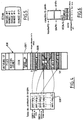
- the terminal architecture according to the invention shown in FIG. 1 comprises a microprocessor (81) connected by an 8-bit data bus to a video circuit (85) for managing the display on a monitor (84) and exchanges with a character generator RAM memory (82), a RAM video type random access memory (VRAM, 83).
- the connection between the microprocessor (81) and the management circuit (85) is done through an 8-bit data bus (8549).
- the connection between the management circuit (85) and the monitor (84) is carried out by a 5-line bus (8530) delivering the red (R), green (V), blue (B), horizontal return (HRTC) signals. ), vertical return (VRT).
- the connection between the management circuit (85) and the character-generating static random access memory (SRAM) (82) is carried out by an address bus (8528) with 14 address lines and by a data bus (8529) 4 lines of data.
- the connection between the management circuit (85) and the VRAM video memory (83) is made on the one hand for the parallel part by an address bus (8547) with 9 address lines and by a local data bus (8546) with 4 data lines and on the other hand for the serial part by a bus of 4 lines (8548).
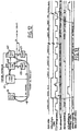
- VRAM is made up of a standard dynamic RAM which is accessed by conventional 'parallel' bus, and a fast static RAM, called serializer, and configured as a shift register that can be read by 'serial bus', all in the same housing ( Figure 3); the coupling between the 2 memories is carried out by bringing a row of words read in the DRAM into contact with the inputs of the shift register, the 'parallel' loading command of the shifter being made at a very precise instant specified by the VRAM in synchronization with the shift clock. It is this simultaneous transfer of all the words in a row on a very 'large bus' internal to VRAM which gives it a large bandwidth. Since VRAM is essentially dynamic RAM, the price of the bit is therefore minimized; of course, its control logic is more complex since it requires a cell refresh automaton and a transfer logic from DRAM to static RAM called 'shifter'.
- FIG. 3 represents the organization of a VRAM video memory in which a part (830) is constituted by a dynamic random access memory of, for example, 256 Kmots of 4 bits, these 256 Kmots being organized in 512 rows of 512 columns.
- a row n (8300) 4 4-bit words constitute the 16 bits of information corresponding to the 8 code bits and the 8 attribute bits defining the code and the attribute (CODATT) of the character to be displayed in a row screen.
- These 4 nibbles are called respectively (CH) for the high code and (CL) for the low code of the character and (AH) for the high attribute, (AL) for the low attribute.
- a memory array slice (8300) is transferred by the bus (832) of 512 x 4 bits to the memory vivid static (831) formed of 512 x 4 bits.
- This memory is in fact made up of 4 registers of 512 bits whose serial outputs constitute the 4 lines of the serial bus (8548).
- a memory slice (8300) allows the storage of 128 CODATT information corresponding to each character of a screen which could, in this way, contain a maximum of 128 columns of characters.
- FIG. 4 represents the logical organization of the dynamic random access memory (830), and FIG. 5 a screen formed by 25 rows of (x) columns of characters, the number of columns being able to vary between 80 and 132.
- the characters can have a dimension between 1 and 15 representation points per slice, each character comprising from 1 to 16 slices in patterns.
- the dynamic memory (830) can be organized so as to contain the interrupt vectors, the registers necessary for the management of stacks, line buffers, the code necessary for the operation of the terminal and, in particular, for the management of the display and communications by a line interface (87) connected by the bus (8549) to the microphone (81) and to the management circuit (85) as shown in Figure 1.
- a 'boot' located in ROM to download to the terminal, via the local network, its presentation program from the data concentrator; in the terminal, this code to be executed by the microphone is housed in the DRAM part of VRAM with the image buffers, which requires a larger memory: rather use a VRAM with a capacity of 256 K x 4.
- a VRAM memory of 64 K x 4 may suffice since the microphone executes the code in ROM only.
- This memory (830) also contains a pointing table (8301) containing, as shown on the left of FIG. 4, the table pointer (83011) and the various row pointers including the current row pointer (8301), these pointers defining the addresses of the rows corresponding to the memory portions such as (8300) for row number 1 for example in which all of the CODATT information corresponding to each of the characters constituting a row for display on the screen are contained in the memory.
- a pointing table (8301) containing, as shown on the left of FIG. 4, the table pointer (83011) and the various row pointers including the current row pointer (8301), these pointers defining the addresses of the rows corresponding to the memory portions such as (8300) for row number 1 for example in which all of the CODATT information corresponding to each of the characters constituting a row for display on the screen are contained in the memory.
- the representation of a character is carried out by 16 sections of 9, 10 or 15 points depending on the size of the character and these representations are stored in the static memory (82) constituting the character generator.
- This information is stored in the form of referenced quartets (nib 0 to nib 3), the number of which depends on the number of points of each character. These quartets are stored at defined addresses in the memory.
- the character H is represented by a matrix of 10 points x 9 lines, the nib 2 quartet of slice 0 will have the value in hexadecimal 8, the nib quartet 1 the hexadecimal value 0 and the quartet nib 0 the hexadecimal value 4.
- Each of these quartets will constitute the 4 pieces of information sent in series on the 4 lines of the bus (8529), this piece of information making it possible to reconstruct the section 0 of the letter H for a 10-point character.
- 3 or 4 nibbles are memorized in the memory 82 according to the size of the character of 8, 9, 10 or 15 points.
- the circuit (85) makes it possible to manage the exchanges between the different constituent elements of the terminal.
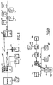
- a first subset constituting the management of transfers between the microphone (81) and the dynamic memory part of the VRAM memory is formed by a logic for managing the write and read transfers (8556, FIG. 2A) between these elements and physical circuits allowing this connection.
- This management logic (8556) generates inter alia the signal SELVRAM (85564) to the sequencer (85477) which supplies the rhythm of the control signals to the VRAM.
- the SELVRAM signal is a simple bus address decoding (8558).
- the physical circuits consist of a multiplexer (8541) connected to the 8 lines of the data bus (8549) of the microphone (81) and receiving on a write multiplexing control input the signal (85561) coming from the management logic. (8556).
- This write multiplexing signal makes it possible to transform the signals arriving on 8 bits by the bus (8549) into 2 signals of 4 bits which are sent from the multiplexer (8541) to a buffer circuit (8542) whose output is connected by a bus 4 lines (8546) to the 4 data entry lines in the dynamic random access memory of VRAM.
- the buffer circuit (8542) is controlled by an ENBUFECR signal for enabling the write buffer (85562) supplied by a second output of the control logic (8556).
- the memory (FIGS.
- This addressing circuit (85472) is addressed by an addressing circuit (85472) connected at output to the address bus of the DRAM (8547) and at input to the address bus of the microphone (8558).
- This addressing circuit (85472) represented in FIG. 2B, comprises a register (85474) connected at the input to the data bus (8549) of the microprocessor (81) and at the output to a multiplexer (854720) to deliver the 8 bits from the top (FETCH-ADDH) of the current row pointer address (8301X). These 8 bits in the upper part are in fact the address of the start of the scoreboard.
- the lower part (FETCH-ADDL) of the current row pointer address is provided by an 8-bit counter (85475) reset to zero by the signal (NF) indicating a new frame, and incremented with each new row of characters by the Fetch-request (FR) signal.
- a NIB logic (85563) from the circuit (8556) makes it possible to address the quartet of the DRAM for the 8 multiplexed buses.
- a 6-stage pipeline (85473) receives the 4 lines of the DRAM parallel data bus (8546) as input.
- This pipeline (85473) stores the 6 quartets (24 bits) defining the address of the next row defined by 16 bits as well as its row attribute defining by 8 bits if the row is double height, double width, at the start slow scrolling, at the end of slow scrolling (smooth scroll) or normal.
- the 16 bits of address of the next row delivered at the output of 4 of the buffers of the pipeline (85473) define at the input of the multiplexer (854720) the signals ROW-SR-ADDL address of low register of row and ROW-SR-ADDH address high row register.
- the outputs of the pipeline defining the 16 address bits are also sent as input to a 16 bit pointer counter (85470, 85471) incremented at the rate of the shift of a character CODATT.
- This pointer counter makes it possible to anticipate the counting of a character, as shown in FIG. 7, on the line (85471).
- This address available at the outlet of the pipeline (85473) is loaded into the pointer counter (85470, 85471) before each start of the screen line by the row transfer signal (85570) (figure 7) and is delivered by the circuit (8557 ) which delivers the control signals (8554) and control of the addressing circuit (85472).
- the sequencer (85477) uses the RTDTR, REF, NLDTR and FR signals to generate the sequences of the RAS, CAS, DT, WE, OE (8554) signals necessary for an operating cycle according to a selected mode of the memory (83). To manage the different modes of access to the VRAM memory, this sequencer also plays the role of arbiter; thus, it generates inter alia the HOLD signal which corresponds to a request to take control of the bus (8549) on the part of the video circuit when one of the signals REF, RTDTR, FR or NLDTR of the circuit (85477) is activated. Receiving the HOLDA acknowledgment signal from the microphone, it thus takes control of the microphone bus (8549) to perform the requested cycle.
- the multiplexer (854720) further includes the input lines CPU-ADDL and CPU-ADDH connected to the address bus of the microprocessor (81) and 3 selection inputs SEL-MAO to SEL-MA2 which allow to select 1 input from 8 to present it at the output of the multiplexer (854720) on the bus (8547).
- selection signals SEL-MAO to SEL-MA2 are also supplied by the circuit (8557).
- the VRAM refresh cycle does not use the circuit multiplexer (854720), because the "CAS before RAS" mode of VRAM is used.
- the last CODATT of row number 2 is the character "G” of the syllable RANG of the word "RANGEE 2", the continuation of which is located at the address of next physical row.
- the following physical row address is determined by cycle 4 using the pointer counter which supplies the address of CODATT "E”. In this way, the serializer continuously receiving clk-decal continuously outputs the CODATT "G", then "E", etc.
- a clock circuit (8550) provides the clock and sequencing signals (8510 to 8514) necessary for the operation of the circuits.
- the data bus (8546) is connected by a buffer register (8543) with 4 inputs and whose 4 outputs are connected to a multiplexer circuit with 2 inputs of 4 lines and 8 parallel outputs.
- the 4 lines of the address bus (8546) are also directly connected to 4 of the inputs of the multiplexing circuit.
- the buffer (8543) allows the storage of the 1st data quartet supplied by the data bus (8546) and wait for the presentation of the 2nd quartet supplied directly by the data bus to the second input quartet of a multiplexer (8544) to validate by the read quartet signal (lect-quart 1) the transmission of the 1st quartet to the multiplexer (8544) and by the read multiplex signal (mux-lect) the transmission of the 8 bits formed by the two quartets to the output of the multiplexer.
- the read multiplexer (mux-read) signal is supplied by the line (85564) coming from the logic circuit (8556).
- the read signal of the 1st quartet is provided by the line (85563) coming from the logic circuit (8556).
- a subset (8500 to 8503) of the management circuit (85) interfaces the 4-line serial bus (8548) with the character generator memory (82).
- This subset consists of 4 buffer registers (8500 - 8501 - 8502 - 8503) mounted in cascades so as to form a pipeline. These buffer registers are controlled by the same clock signal CLK-CODATT delivered by the line (8510) of the sequencing circuit (8550).
- CLK-CODATT delivered by the line (8510) of the sequencing circuit (8550).
- the outputs of the registers respectively contain the low attributes (AL), the high attributes (AH), the low code (CL) and the high code (CH) of a character of the column (x) of the row (y).
- the 4 output lines of the first buffer register (8500) memorizing the last quartet sent by the memory, are sent to a second buffer register (8506) which will thus store the top quartet of the character code CH (3: 0) in synchronism with the clock signal (8510) CLK-CODATT.
- the outputs of the third buffer register (8502) storing the second quartet emitted by the memory are sent to an additional buffer register (8504) making it possible to store the quartet of high attribute AH (3: 0) of the attributes of the character.
- the AL (3: 0) attribute and CL (3: 0) code quartets of each character are provided directly by the second and third buffer registers (8501 - 8503).
- the 8 lines formed by the 4 ATT lines (7: 4) provided by the register (8504) and the 4 AL lines (3: 0) by the register (8503) constitute the 8 attribute lines sent to the attribute controller (853 ).
- the 4 COD lines (7: 4) of top quartet of the character code delivered by the output of the buffer (8506) are combined with 4 lines (8508) providing the pattern number, with 4 other lines (8507) output from the second buffer register (8501) delivering the low quartets CL (3: 0) of the character code COD (3: 0) and with 2 lines (8509) providing the quartet number of the section to constitute a 14-line bus (8528) commanding the addresses of the random access memory (82).
- the quartet number of the slice corresponds to the elements called nib.
- the first counter (8552) is a modulo 4 counter while the second is a counter modulo 16 configurable according to the number of slices or patterns of a character.
- the static memory also receives by the lines (85530) the control signals supplied by the control logic (8553) and consisting of the signals CS circuit selection, WE write read, OE validation of the outputs.
- the memory output (82) is interfaced with the monitor (84) by a sub-assembly made up of 4 4-bit buffer registers (8520 to 8523) connected in cascades so as to constitute a pipeline and controlled synchronously by a signal clk-gcq clock supplied by the output line (8511) of the sequencing circuit (8550).
- the 4 outputs (8527) of the first buffer register (8523) are sent to 4 inputs of the attribute controller (853) and constitute the down / down quartet (QLL) of the 16 bits of each character slice.
- the 4 outputs (8526) of the second buffer register (8522) are sent to the following 4 lines and constitute the low / high quartet (QLH) of the 16 points making up a character range.
- the outputs (8525) of the third register (8521) are connected to 4 other circuit input lines (853) and constitute the high / low quartets (QHL) of the 16 points of a character slice and finally the 4 lines of output (8524) from the fourth register (8520) are sent to the other 4 input lines of the video attribute controller (853) to constitute the up / up quartet (QHH) of the 16 points of a character slice.
- the attribute controller circuit (853) also receives an ech-pattern clock signal from the line (8512) of the sequencing circuit (8550).
- the attribute controller in addition to the 3 lines (8530) delivers an output (HRTC) horizontal return and an output (VRT) vertical return to the monitor (84).
- a controller loads the table start address of the addresses of character rows in the current row pointer buffer (85473); the latter will be reloaded before each start of a new row of characters with the address of the start of the next row from the table of row pointers (FIGS. 4 and 7). Then, during the horizontal returns of each active video line, a command to transfer this buffer both to the inputs of the 'pointer' counter (85470, 85471) and to the pointer of the VRAM then makes it possible to communicate this current row start address in the shift register, the latter being ready to shift the CODATT words from the loaded address.
- the shifter which outputs on the VRAM serial bus the CODATT (i) is validated for i varying from 1 to 132 for example.
- Any given row N (8300) of the VRAM contains 512 nibbles (figure 3), numbered from 0 to 511, ie 256 bytes which can accommodate 128 CODATT maximum of 16 bits; in the case of the display mode in 132 characters per line, we are led to reloading 'in real time' during the video line in order to complete the CODATTs of the current row of characters.
- an end of row detection threshold determined by the circuit is fixed (85476); when the outputs of the 'pointer' counter in row N of the VRAM coincide with this threshold, an automaton initiates a 'real time' transfer request RTDTR in order to transfer the row N + 1 of the VRAM.
- This transfer which takes place at a very precise time specified by the VRAM must be synchronous with the end of serialization of the last datum, namely the 511th quartet of row N of the VRAM; once the loading has been executed, the shifter then begins to output the following CODATT data from the first quartet 0 of row N + 1 of the VRAM.
- the ATT attribute is sent to the attribute controller (853) and the COD code is associated with the character slice number or pattern number), supplemented by an address defining high or low nibble; this 13-bit GC address makes it possible to extract the current character pattern of the character generator from a 4-bit bus SRAM memory, all in the unit of time of a character (FIG. 7).
- a command to the attribute controller informs it that a couple [ATT (7: 0)] (i) and [MOTIF (15: 0) ] (i) (or MOTIF (8: 0) for 132 columns) associated with the character i of the screen is available; the attribute controller then samples it and then processes it (see also patent number EP87400711.5 of 01.04.87) into R, G, B signals intelligible by the cathode-ray tube monitor.
- the sampling frequency of the attribute controller obviously follows the character frequency.
- the reference (130) represents the scanning control signals with the reference (1300) representing the vertical return signal delivered by the VRT output and the references (1301) representing the horizontal return signals delivered by the HRTC output.
- the reference (8301x) represents the current row pointer and its evolution over time.
- the reference (8508) represents the value of the slice or pattern number evolving between 0 and 11 in the case of a character comprising 12 slices.
- the reference (85470) represents the loading of the pointer counter with the value of the pointer of current row, this before carrying out a transfer of rows, and serializing this row then.
- each row has 132 characters and the address of the character to be displayed is determined by adding to the value of the row pointer (85470) the value of a modulo 4 counter which gives the least significant addresses of the character.
- a modulo 4 counter which gives the least significant addresses of the character.
- To this low weight part defining the number of the character in the column there is a second low weight part constituted by the output of the counter (85471) which defines the address of the quartet of the word CODATT addressed in the memory, this word CODATT being made up of 4 quartets.
- the pointer counter assembly consists of the counters (85470 -85471) and operates at the same frequency as the CLK-CODATT character clock.
- the counter (85471) carries out a counting anticipation which makes it possible to know the address of the first quartet of CODATT as soon as the character pointer of the next column in the same row is loaded.
- the character quartets are transferred from the VRAM to the SRAM by the commands of the cycle control circuit (8557) and are shifted in series at the rate of the clock clk-decal represented by the line (85131) consisting of the output of a counter 85230 modulo n which can be parameterized between 0 and 132 and whose clock input receives a clock signal of frequency (8513) corresponding to that of the signal clk-decal.
- the 4 quartets output in series are temporarily stored in the buffer registers (8500 to 8503) at the rate of the clk-codatt clock represented by the line (8510). This clock corresponds to a signal of the same frequency as the clk-decal clock but offset by a period.
- the lines (8500 to 8503) represent the contents of the corresponding buffers of Figure 2 at the time of character processing. These lines also represent the shift of the characters in time as a function of the clock signal clk-codatt so that at the time of the appearance of the ech-cod-att pulses corresponding to the character 0 represented by the arrows 134, 135, 136 the quartets of this character CH-O, CL-O, AH-O, AL-O are found respectively in the registers (8500 - 8501 - 8502 - 8503).
- the transfer of the characters CH-O and AH-O takes place in the buffer registers (8504 - 8506) and the attributes of the character O appear at the input of the circuit (853) while the character code O is combined with the pattern number and the digitized character quartet number to serve as an address for addressing the RAM memory (82).
- the quartet number is provided by a counter (8552) receiving a clock signal (8511) of the same frequency as the clock signal clk-gcq but shifted forward by half a period.
- This counter (8552) can be configured between 0 and 4 to count a number of nibbles depending on the number of dots represented in a character range.
- the pattern number is provided by the output (8508) of the circuit (8551) which is actually a character slice counter which can be set between 0 and 16, this pattern number counter being incremented by 1 each time the quartet counter will have reached the maximum value for which it has been set.
- the control circuit (855) supplies via the control part (8553) the signals CS; WE and OE necessary for the operation of the RAM (82) in reading and this delivers on the bus (8529) the data constituting the points of a slice of a character.
- These data are provided in the form of quartets called QLL QLH QHL QHH which are loaded progressively into the buffer registers (8520 to 8523) at the rate of the clock clk-gcq supplied by the line (8511).
- a synchronization signal (8512) providing the ech-pattern signal and constituted by the output of a programmable counter as a function of the number of display points of a character, in this case here 9.
- This signal makes it possible to carry out the transfer of the quartets from the buffer registers to the attribute controller when the character points necessary for display have been stored.
- the QHH quartet is not used and for this reason, it has not been represented on line (8529) of the diagram in FIG. 13.
Landscapes
- Engineering & Computer Science (AREA)
- Theoretical Computer Science (AREA)
- Physics & Mathematics (AREA)
- General Physics & Mathematics (AREA)
- Computer Hardware Design (AREA)
- Human Computer Interaction (AREA)
- General Engineering & Computer Science (AREA)
- Controls And Circuits For Display Device (AREA)
- Digital Computer Display Output (AREA)
Applications Claiming Priority (2)
| Application Number | Priority Date | Filing Date | Title |
|---|---|---|---|
| FR9014366A FR2669448B1 (fr) | 1990-11-19 | 1990-11-19 | Architecture de terminal et circuit de gestion. |
| FR9014366 | 1990-11-19 |
Publications (2)
| Publication Number | Publication Date |
|---|---|
| EP0487400A1 EP0487400A1 (fr) | 1992-05-27 |
| EP0487400B1 true EP0487400B1 (fr) | 1996-06-05 |
Family
ID=9402328
Family Applications (1)
| Application Number | Title | Priority Date | Filing Date |
|---|---|---|---|
| EP91403100A Expired - Lifetime EP0487400B1 (fr) | 1990-11-19 | 1991-11-18 | Architecture de terminal et circuit de gestion |
Country Status (7)
| Country | Link |
|---|---|
| US (1) | US5799202A (enExample) |
| EP (1) | EP0487400B1 (enExample) |
| JP (1) | JP3233666B2 (enExample) |
| KR (1) | KR0135070B1 (enExample) |
| DE (1) | DE69120034T2 (enExample) |
| FR (1) | FR2669448B1 (enExample) |
| TW (1) | TW263572B (enExample) |
Families Citing this family (7)
| Publication number | Priority date | Publication date | Assignee | Title |
|---|---|---|---|---|
| US6078316A (en) * | 1992-03-16 | 2000-06-20 | Canon Kabushiki Kaisha | Display memory cache |
| US6160561A (en) * | 1996-09-12 | 2000-12-12 | Micron Electronics, Inc. | Method for displaying data on a video display |
| US5867140A (en) * | 1996-11-27 | 1999-02-02 | Motorola, Inc. | Display system and circuit therefor |
| US6247088B1 (en) * | 1998-05-08 | 2001-06-12 | Lexmark International, Inc. | Bridgeless embedded PCI computer system using syncronous dynamic ram architecture |
| JP3660150B2 (ja) | 1999-02-08 | 2005-06-15 | シャープ株式会社 | プリントデータ制御方法及び情報処理システム |
| JP4942012B2 (ja) * | 2005-05-23 | 2012-05-30 | ルネサスエレクトロニクス株式会社 | 表示装置の駆動回路、および駆動方法 |
| US9705620B2 (en) * | 2015-09-18 | 2017-07-11 | Qualcomm Incorporated | Synchronization of endpoints using tunable latency |
Family Cites Families (23)
| Publication number | Priority date | Publication date | Assignee | Title |
|---|---|---|---|---|
| US4342095A (en) * | 1979-04-02 | 1982-07-27 | Harris Corporation | Computer terminal |
| US4363108A (en) * | 1979-06-25 | 1982-12-07 | Honeywell Information Systems Inc. | Low cost programmable video computer terminal |
| US4404554A (en) * | 1980-10-06 | 1983-09-13 | Standard Microsystems Corp. | Video address generator and timer for creating a flexible CRT display |
| DE3138930C2 (de) * | 1981-09-30 | 1985-11-07 | Siemens AG, 1000 Berlin und 8000 München | Datensichtgerät |
| US4549172A (en) * | 1982-06-21 | 1985-10-22 | Motorola, Inc. | Multicolor display from monochrome or multicolor control unit |
| US4631699A (en) * | 1982-11-30 | 1986-12-23 | Honeywell Information Systems Inc. | Firmware simulation of diskette data via a video signal |
| US4866600A (en) * | 1983-04-27 | 1989-09-12 | Tandy Corporation | Computer video control system |
| US4646261A (en) * | 1983-09-27 | 1987-02-24 | Motorola Computer Systems, Inc. | Local video controller with video memory update detection scanner |
| US4642794A (en) * | 1983-09-27 | 1987-02-10 | Motorola Computer Systems, Inc. | Video update FIFO buffer |
| US4646077A (en) * | 1984-01-16 | 1987-02-24 | Texas Instruments Incorporated | Video display controller system with attribute latch |
| US4862156A (en) * | 1984-05-21 | 1989-08-29 | Atari Corporation | Video computer system including multiple graphics controllers and associated method |
| US4604743A (en) * | 1984-11-21 | 1986-08-05 | North American Philips Corporation | Bus structure for an image processor |
| US4858107A (en) * | 1985-03-11 | 1989-08-15 | General Electric Company | Computer device display system using conditionally asynchronous memory accessing by video display controller |
| JPS6365486A (ja) * | 1986-09-08 | 1988-03-24 | ミノルタ株式会社 | デイスプレイ表示装置 |
| US5001652A (en) * | 1987-03-20 | 1991-03-19 | International Business Machines Corporation | Memory arbitration for video subsystems |
| GB2202720B (en) * | 1987-03-27 | 1991-04-17 | Ibm | Raster scan display system with random access memory character generator |
| US5319786A (en) * | 1987-05-20 | 1994-06-07 | Hudson Soft Co., Ltd. | Apparatus for controlling a scanning type video display to be divided into plural display regions |
| JPS641033A (en) * | 1987-06-24 | 1989-01-05 | Toshiba Corp | Computer device |
| US5151997A (en) * | 1989-08-10 | 1992-09-29 | Apple Computer, Inc. | Computer with adaptable video circuitry |
| US4965670A (en) * | 1989-08-15 | 1990-10-23 | Research, Incorporated | Adjustable overlay display controller |
| US5227863A (en) * | 1989-11-14 | 1993-07-13 | Intelligent Resources Integrated Systems, Inc. | Programmable digital video processing system |
| US5341470A (en) * | 1990-06-27 | 1994-08-23 | Texas Instruments Incorporated | Computer graphics systems, palette devices and methods for shift clock pulse insertion during blanking |
| DE69132209T2 (de) * | 1991-07-24 | 2000-09-28 | Texas Instr France Villeneuve | Anzeigeadapter |
-
1990
- 1990-11-19 FR FR9014366A patent/FR2669448B1/fr not_active Expired - Fee Related
-
1991
- 1991-11-15 TW TW080108975A patent/TW263572B/zh active
- 1991-11-18 DE DE69120034T patent/DE69120034T2/de not_active Expired - Fee Related
- 1991-11-18 EP EP91403100A patent/EP0487400B1/fr not_active Expired - Lifetime
- 1991-11-19 KR KR1019910020587A patent/KR0135070B1/ko not_active Expired - Lifetime
- 1991-11-19 JP JP30361791A patent/JP3233666B2/ja not_active Expired - Lifetime
-
1997
- 1997-04-16 US US08/839,102 patent/US5799202A/en not_active Expired - Lifetime
Non-Patent Citations (1)
| Title |
|---|
| IBM TECHNICAL DISCLOSURE BULLETIN vol. 26, no. 4, Septembre 1983, NEW YORK (US) pages 2156 - 2158; G.J.BARNETT ET AL.: 'Direct Extraction of Data from the Refresh Buffer of a Display'* page 2157, ligne 10 - ligne 29; figure 1 *. * |
Also Published As
| Publication number | Publication date |
|---|---|
| JPH06242752A (ja) | 1994-09-02 |
| EP0487400A1 (fr) | 1992-05-27 |
| US5799202A (en) | 1998-08-25 |
| FR2669448A1 (fr) | 1992-05-22 |
| FR2669448B1 (fr) | 1993-01-15 |
| DE69120034D1 (de) | 1996-07-11 |
| KR920010414A (ko) | 1992-06-26 |
| KR0135070B1 (ko) | 1998-05-15 |
| DE69120034T2 (de) | 1996-11-14 |
| TW263572B (enExample) | 1995-11-21 |
| JP3233666B2 (ja) | 2001-11-26 |
Similar Documents
| Publication | Publication Date | Title |
|---|---|---|
| FR2566951A1 (fr) | Procede et systeme pour l'affichage d'informations visuelles sur un ecran par balayage ligne par ligne et point par point de trames video | |
| FR2599873A1 (fr) | Systeme d'affichage video | |
| FR2650902A1 (fr) | Ordinateur avec circuit integre video pilote par memoire vive | |
| JPS646477B2 (enExample) | ||
| FR2511789A1 (fr) | Systeme de tamponnage de ligne pour l'affichage d'images multiples dans un jeu video | |
| AU710656B2 (en) | Address generating apparatus, picture display apparatus, address generating method and picture displaying method | |
| FR2604019A1 (fr) | Dispositif d'affichage video couleur pour systeme d'ordinateur, et procede de conversion de signaux video couleur a cet effet | |
| EP0487400B1 (fr) | Architecture de terminal et circuit de gestion | |
| JP2007535006A (ja) | システムメモリへのgpuのレンダリング | |
| FR2566949A1 (fr) | Systeme d'affichage d'images video sur un ecran a balayage ligne par ligne et point par point | |
| FR2542113A1 (fr) | Generateur de graphiques a ordinateur | |
| FR2680890A1 (fr) | Antememoire configurable et systeme de traitement d'images contenant une telle antememoire. | |
| EP0202166A1 (fr) | Circuit de mémoire d'image virtuelle permettant le multifenêtrage | |
| US5710604A (en) | Video memory device for color-sequential-type displays | |
| JPH0740179B2 (ja) | 表示制御装置 | |
| FR2491651A1 (fr) | Ensemble a memoire pour le transfert de donnees vers un dispositif de visualisation a tube a rayon cathodique | |
| JPH11510620A (ja) | 統合されたシステム/フレームバッファメモリ及びシステム、ならびにそれらの使用方法 | |
| US5929868A (en) | Method and apparatus for computer display memory management | |
| US6128032A (en) | Method for scrolling a video signal in an internet set top box | |
| EP0255436B1 (fr) | Carte graphique et interface clavier souris | |
| EP0020244B1 (fr) | Procédé et dispositif pour l'adressage d'une mémoire d'image dans un système de télétexte | |
| BE1001069A3 (fr) | Systeme d'affichage a balayage de trame avec generateur de caracteres a memoire a acces aleatoire. | |
| FR2463555A1 (fr) | Dispositif d'affichage permanent d'information graphique sur un ecran de television et de transmission simultanee sur ligne telephonique | |
| KR950012663B1 (ko) | 크로스바 망을 이용한 화상 시스템 및 그 시스템의 엑세스 제어방법 | |
| JP3251394B2 (ja) | データ転送装置、受信装置およびゲーム装置 |
Legal Events
| Date | Code | Title | Description |
|---|---|---|---|
| PUAI | Public reference made under article 153(3) epc to a published international application that has entered the european phase |
Free format text: ORIGINAL CODE: 0009012 |
|
| 17P | Request for examination filed |
Effective date: 19920125 |
|
| AK | Designated contracting states |
Kind code of ref document: A1 Designated state(s): DE ES FR GB IT SE |
|
| RAP3 | Party data changed (applicant data changed or rights of an application transferred) |
Owner name: BULL S.A. |
|
| 17Q | First examination report despatched |
Effective date: 19940616 |
|
| GRAH | Despatch of communication of intention to grant a patent |
Free format text: ORIGINAL CODE: EPIDOS IGRA |
|
| GRAA | (expected) grant |
Free format text: ORIGINAL CODE: 0009210 |
|
| AK | Designated contracting states |
Kind code of ref document: B1 Designated state(s): DE ES FR GB IT SE |
|
| PG25 | Lapsed in a contracting state [announced via postgrant information from national office to epo] |
Ref country code: ES Free format text: THE PATENT HAS BEEN ANNULLED BY A DECISION OF A NATIONAL AUTHORITY Effective date: 19960605 |
|
| REF | Corresponds to: |
Ref document number: 69120034 Country of ref document: DE Date of ref document: 19960711 |
|
| GBT | Gb: translation of ep patent filed (gb section 77(6)(a)/1977) |
Effective date: 19960701 |
|
| GRAH | Despatch of communication of intention to grant a patent |
Free format text: ORIGINAL CODE: EPIDOS IGRA |
|
| ITF | It: translation for a ep patent filed | ||
| PG25 | Lapsed in a contracting state [announced via postgrant information from national office to epo] |
Ref country code: SE Effective date: 19960905 |
|
| PLBE | No opposition filed within time limit |
Free format text: ORIGINAL CODE: 0009261 |
|
| STAA | Information on the status of an ep patent application or granted ep patent |
Free format text: STATUS: NO OPPOSITION FILED WITHIN TIME LIMIT |
|
| 26N | No opposition filed | ||
| REG | Reference to a national code |
Ref country code: GB Ref legal event code: IF02 |
|
| PGFP | Annual fee paid to national office [announced via postgrant information from national office to epo] |
Ref country code: GB Payment date: 20061026 Year of fee payment: 16 |
|
| PGFP | Annual fee paid to national office [announced via postgrant information from national office to epo] |
Ref country code: DE Payment date: 20061108 Year of fee payment: 16 |
|
| PGFP | Annual fee paid to national office [announced via postgrant information from national office to epo] |
Ref country code: IT Payment date: 20071117 Year of fee payment: 17 |
|
| GBPC | Gb: european patent ceased through non-payment of renewal fee |
Effective date: 20071118 |
|
| PG25 | Lapsed in a contracting state [announced via postgrant information from national office to epo] |
Ref country code: DE Free format text: LAPSE BECAUSE OF NON-PAYMENT OF DUE FEES Effective date: 20080603 |
|
| PG25 | Lapsed in a contracting state [announced via postgrant information from national office to epo] |
Ref country code: GB Free format text: LAPSE BECAUSE OF NON-PAYMENT OF DUE FEES Effective date: 20071118 |
|
| PG25 | Lapsed in a contracting state [announced via postgrant information from national office to epo] |
Ref country code: IT Free format text: LAPSE BECAUSE OF NON-PAYMENT OF DUE FEES Effective date: 20081118 |
|
| PGFP | Annual fee paid to national office [announced via postgrant information from national office to epo] |
Ref country code: FR Payment date: 20101217 Year of fee payment: 20 |