EP0487025A1 - Steckverbinder für Leitungskabel - Google Patents
Steckverbinder für Leitungskabel Download PDFInfo
- Publication number
- EP0487025A1 EP0487025A1 EP91119716A EP91119716A EP0487025A1 EP 0487025 A1 EP0487025 A1 EP 0487025A1 EP 91119716 A EP91119716 A EP 91119716A EP 91119716 A EP91119716 A EP 91119716A EP 0487025 A1 EP0487025 A1 EP 0487025A1
- Authority
- EP
- European Patent Office
- Prior art keywords
- plug
- projection
- receiver
- fitting portion
- pressure
- Prior art date
- Legal status (The legal status is an assumption and is not a legal conclusion. Google has not performed a legal analysis and makes no representation as to the accuracy of the status listed.)
- Granted
Links
Images


Classifications
-
- H—ELECTRICITY
- H02—GENERATION; CONVERSION OR DISTRIBUTION OF ELECTRIC POWER
- H02G—INSTALLATION OF ELECTRIC CABLES OR LINES, OR OF COMBINED OPTICAL AND ELECTRIC CABLES OR LINES
- H02G15/00—Cable fittings
- H02G15/08—Cable junctions
- H02G15/18—Cable junctions protected by sleeves, e.g. for communication cable
- H02G15/184—Cable junctions protected by sleeves, e.g. for communication cable with devices for relieving electrical stress
-
- H—ELECTRICITY
- H01—ELECTRIC ELEMENTS
- H01R—ELECTRICALLY-CONDUCTIVE CONNECTIONS; STRUCTURAL ASSOCIATIONS OF A PLURALITY OF MUTUALLY-INSULATED ELECTRICAL CONNECTING ELEMENTS; COUPLING DEVICES; CURRENT COLLECTORS
- H01R13/00—Details of coupling devices of the kinds covered by groups H01R12/70 or H01R24/00 - H01R33/00
- H01R13/46—Bases; Cases
- H01R13/53—Bases or cases for heavy duty; Bases or cases for high voltage with means for preventing corona or arcing
Definitions
- the present invention relates to a cable plug for high voltage usage, or a high-voltage plug. More particularly, this invention relates to a plug for connecting a power cable to an electric device which is operated at voltage of 1 kv to several 10 kv.
- insulating rubbers and other organic materials such as polyethylene have been used.
- a dielectric strength of these materials is apt to change with applied pressure thereto as shown in Fig.3. Namely, the dielectric strength increases as the pressure becomes large until the pressure reaches a certain value.
- conventional high-voltage plugs are provided with means for increasing the dielectric strength of such insulating materials by applying suitable pressure thereto. Two typical examples of such conventional high-voltage plugs are explained here.
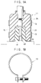
- FIGS 1A and 1B show structures of a conventional plug 11, a plug receiver 15 and ribbon-shape bands 13.
- the bands 13 are provided on the outer surface of the plug 11 to apply pressure to an insulating material incorporated therein.
- a pair of plug receivers 15 for electrical connection are provided on the electric device 12, and each receiver 15 is formed into a projection and comprises a contact terminal 17 and an insulating material 19 provided around the terminal 17.
- a cavity portion 21 of the plug 11 is fitted around these projections 15 so as to connect its contact terminal 23 to the contact terminals 17. Accordingly, it is possible to apply pressure to the insulating material 19 by compressing the plug 11 with the bands 13 from the outside. As a result, the dielectric strength of the material 19 can be increased.
- Fig.2 shows another conventional example. As shown in the same drawing, this case has an epoxy bushing 31 to which a protection tube 33 is secured with several screws. Moreover, the protection tube 33 has springs 35 for applying pressure to a semiconductive rubber layer 39 and an insulating rubber 41 through a metal plate 37.
- the present invention was made to solve the above-mentioned problem in the conventional technology, therefore, it is an object thereof to provide a high-voltage plug which can be easily handled and is excellent in the insulating ability.
- the present invention is characterized by a plug for performing electrical connection with being fitted around a plug receiver which includes power receiving means and is formed into a projection, comprising an electrically conductive part which is connected to a core wire of a power supply cable and has a connection part for connecting it to a contact terminal of the plug receiver, a semiconductive layer part which is provided around the conductive part so as to prevent from high voltages centering in small parts of the plug , an insulating layer part which is provided on the exterior of the semi-conductive layer part so as to protect an outer case from high voltages of the outer surface of the semi-conductive layer part, a fitting portion comprising a cavity which is fitted around the plug receiver so as to facilitate connection between the contact terminal of the plug receiver and the conductive part of the plug, pressurizing means for increasing a dielectric strength of the insulating layer part by pressure to be generated by slightly lessening the inner dimension of the fitting portion as compared with the outer dimension of the plug receiver, pressure control means for making the pressure to be uniform by changing the dimensions ,
- the above mentioned pressure control means is the most important element of the present invention. According to the above described construction of the present invention, it becomes possible to reduce the number of parts necessary for the plug system and facilitate attachment of the plug.
- Fig.4 shows schematic construction of a system utilizing the embodiment of the present invention.
- a high-voltage electric device not shown is contained in a box 51, and plug receivers 53 formed into a pair of projections are mounted on the box 51.
- the bottom end portion of an L-shape plug 55 is fitted to make electrical contact relation therewith.
- each plug 55 is connected to a power cable 57 comprising a 22 kv high-voltage crosslinking polyethylene cable at the right or left end portion thereof.
- these two plugs 55 have completely the same structure.
- Fig.5 shows a detailed cross section of the structure of the plug 55.
- the plug 55 is provided with an insulating layer 61 consisting of an L-shape insulating rubber material.
- a semi-conductive layer 63 consisting of an L-shape hard rubber material is embedded.
- the semiconductive layer 63 is provided coaxially to the upper central axis thereof with a copper conductive part 65 in which the left half portion is solid, but the right half portion is hollow.
- the conductive part 65 is electrically connected to a core wire 57a of the power cable 57 through a contact piece not shown in the same drawing. While, the left end portion of the conductive part 65 has a flat lower face and contains a female screw extending vertically in the same drawing at the central portion thereof. Moreover, the female screw is engaged with an upper male screw portion 67c of a contact terminal 67 which further includes a cylindrical lower portion 67a and a hexagonal-prism intermediate portion 67b.
- a truncated-cone-shape fitting portion 69 opening downwards is provided coaxially to the contact terminal 67 in the left end portion of the insulating layer 61.
- the upper portion 69a of the fitting portion 69 is formed with an annular portion 63a of the semiconductive layer 63, and the intermediate portion 69b is constructed with the insulating layer 61.
- the upper portion 69a and the intermediate portion 69b of the fitting portion 69 are connected to each other so as to form a continuous or the same side face of a truncated cone.
- a grounded outer cover 71 is provided on the outer surface of the insulating layer 61.
- the left bottom end portion of the cover 71 has a convex portion 71a with a substantially trapezoidal cross section on the inner circumference thereof as well as covers the left bottom end portion of the insulating layer 61.
- the power cable 57 is inserted into the plug 55 so as to connect the core wire 57a of the cable 57 with the conductive part 65 described above.
- an insulating tape 73 is wound around the right end portion of the outer cover 71.
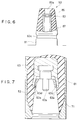
- Fig.6 shows a cross section of the plug receiver 53 to be fitted around in the above mentioned plug 55.
- the plug receiver 53 is mounted on an attachment base 81 of the box 51, and comprises a truncated-cone projection 83 consisting of an epoxy resin and extending upwards from the base 81.
- the projection 83 has a side face with the same inclination as that of the above-mentioned fitting portion 69 comprising the insulating layer 61 and semi-conductive layer 63, and the outer diameter of the former 83 is slightly larger (by about 2mm) than the inner diameter of the latter 69.
- a trapezoidal groove 83c with a diameter slightly larger (by about 2mm) than that of the above mentioned convex portion 71a is formed in the bottom end portion of the fitting portion 69. Therefore, the groove 83c serves as holding means for engaging the plug 55 with the plug receiver 53.
- a cylindrical hole 83a is formed in the projection 83 coaxially to the central axis thereof, and a cylindrical metal piece 87 is embedded in the inner wall of the hole 83a.
- a contact ring 85 electrically connecting to the metal piece 87 is provided at the intermediate portion of the hole 83.
- the bottom end of the metal piece 87 is connected to an input terminal of the above-described electric device.
- an insulating rubber material is used for producing the insulating layer 61
- a hard rubber material is used for the semi-conductive layer 63
- the conductive part 65 is made of copper
- the projection 83 of the plug receiver 53 consists of an epoxy resin.
- the pressure to be generated on the contact face between the plug 55 and the plug receiver 53 on engaging them with each other is adjusted at about several kg/cm2, for example, by setting the difference between the outer diameter of the projection 83 and the inner diameter of the fitting portion 69 at 1mm.
- the left lower portion of the insulating layer 61 interposed between the compression band and the projection 83 is compressed by both of the compression force of the band and the pressure generated by engagement of the fitting portion 69 and the projection 83. Therefore, the dielectric strength is elevated so that sufficient insulation ability of the insulating layer 61 can be guaranteed.
- the inner circumference of the annular portion 63a should be uniformly extended at the fitting part when the projection 83 is inserted in the fitting portion 69 of the plug 55, if both ends of the annular portion 63a were free.
- the base potion of the annular portion 63a is rigidly fixed with the body of the semiconductor layer 63, the base potion is little extended. Therefore, stress is generated only at the base portion , so that the portion 63a is deformed as shown in Fig.7 for the reason that will be explained below. That is, the annular portion 63a is bent more than the inclination angle of the side face of the truncated cone decided by the projection 83, and thereby a small gap 63d is formed between them.
- the structure of the semiconductive layer 63 is symmetrical about the central axis thereof, considering a sliced part cut off from the annular portion 63a by a very small length in a circular direction, then a deflection of the part is nearly equal to that of a cantilever applied with a force F1 caused by inserting the projection 83 into the annular portion 63a.
- the cantilever is bent to the deflection curve ⁇ 1 shown in Fig. 8A. And the deflection ⁇ 1 of the part causes a compression force F2 on the insulating layer 61 surrounding the annular portion 63a, which produce the reaction force F2 on the cantilever as shown in Fig. 8B. Then, the cantilever is also bent downwards to the deflection curve shown in the same figure. As a result, the cantilever is deformed into the the deflection curve ( ⁇ 1- ⁇ 2) as shown in Fig. 8C.
- the above-mentioned small gap 63d is generated between the annular portion 63a and the projection 83.
- a circular stress is also caused in the annular portion 63a by being extended in a circular direction, however it is not considered in the above discussion because of smallness of its influence to the deflection of the cantilever.
- the second embodiment of the present invention is so improved that the gap due to the insertion of the projection can be prevented, and preferred insulating ability can be maintained over a long term.
- the inclination gradient of the inner side wall of the annular portion 63a is set slightly larger as shown by the solid line in Fig.9 by enlarging the diameter of the top end portion thereof as compared with that in the first embodiment as shown by the dotted line in the same drawing.
- the force F1' applies to the cantilever instead of F1 when the projection inserts into annual portion 63a, which deflects the cantilever to the curve ⁇ 1' having an upward concave as shown in Fig.10C. And this deflection causes a force F2' as the same principle as described above, which bent the cantilever to the deflection curve ⁇ 2'. Therefore the cantilever, as a result, is bent in the deflection curve ( ⁇ 1'- ⁇ 2') shown in Fig. 10D. However, since ( ⁇ 1'- ⁇ 2') is nearly equal to zero at any points of the cantilever, the gap as above mentioned is not generated. As a result, discharge between the annular portion 63a and the projection 58 is not caused.
- the cable plug based on the construction of the second embodiment can prevent the gap generation between the annular portion 63a and the projection 83 as shown in Fig.7, it can maintain preferred insulating ability over a long period of time.
- the same effect can be obtained by modifying the outer diameter of the distal end portion of the projection 83.
- the inclination of the side wall of the projection 83 may be decreased by reducing the diameter of the distal end portion by about 1.6 mm.
- annular portion 63a may be changed into a curve.
- the fitting portion may be also applied to T-shape, Y-shape or cross-type cable plugs.
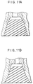
- the shape of the fitting portion is not limited to the truncated cone type, but the portion may be formed in a shape with a narrow skirt portion as shown in Fig.11(a) or in a shape with a wide skirt portion as shown in Fig.11(b).
Landscapes
- Connector Housings Or Holding Contact Members (AREA)
Applications Claiming Priority (2)
| Application Number | Priority Date | Filing Date | Title |
|---|---|---|---|
| JP312721/90 | 1990-11-20 | ||
| JP2312721A JP2866473B2 (ja) | 1990-11-20 | 1990-11-20 | ケーブルプラグ |
Publications (2)
| Publication Number | Publication Date |
|---|---|
| EP0487025A1 true EP0487025A1 (de) | 1992-05-27 |
| EP0487025B1 EP0487025B1 (de) | 1995-04-19 |
Family
ID=18032622
Family Applications (1)
| Application Number | Title | Priority Date | Filing Date |
|---|---|---|---|
| EP19910119716 Expired - Lifetime EP0487025B1 (de) | 1990-11-20 | 1991-11-19 | Steckverbinder für Leitungskabel |
Country Status (3)
| Country | Link |
|---|---|
| EP (1) | EP0487025B1 (de) |
| JP (1) | JP2866473B2 (de) |
| DE (1) | DE69109060T2 (de) |
Cited By (6)
| Publication number | Priority date | Publication date | Assignee | Title |
|---|---|---|---|---|
| WO1994002977A1 (de) * | 1992-07-25 | 1994-02-03 | Karl Pfisterer Elektrotechnische Spezialartikel Gmbh & Co. Kg | Kabelstecker |
| WO1994002976A1 (de) * | 1992-07-25 | 1994-02-03 | Karl Pfisterer Elektrotechnische Spezialartikel Gmbh & Co. Kg | Winkelstecker |
| WO1996019024A1 (en) * | 1994-12-12 | 1996-06-20 | N.V. Raychem S.A. | Sealing device |
| EP0716488A3 (de) * | 1994-12-08 | 1997-02-19 | Ritz Messwandler Kg | Hochspannungssteckkontakt |
| EP2490302A1 (de) * | 2011-02-15 | 2012-08-22 | GE Sensing & Inspection Technologies GmbH | Hochspannungs-Steckverbindungsteil für ein Hochspannungskabel und Verfahren zur Herstellung desselben |
| WO2014084052A1 (ja) * | 2012-11-28 | 2014-06-05 | 株式会社オートネットワーク技術研究所 | L字型端子金具およびそれを用いたl字型コネクタ |
Families Citing this family (4)
| Publication number | Priority date | Publication date | Assignee | Title |
|---|---|---|---|---|
| KR20130059564A (ko) * | 2011-11-29 | 2013-06-07 | 엘지이노텍 주식회사 | 방수구조를 가지는 터미널 케이블 조립체 |
| JP6438675B2 (ja) * | 2014-04-28 | 2018-12-19 | 矢崎総業株式会社 | コネクタの防水構造 |
| CN111682500B (zh) * | 2020-06-28 | 2022-05-06 | 中科英华长春高技术有限公司 | 一种海上风电用35kV可分离连接器 |
| EP4167391A1 (de) * | 2021-10-13 | 2023-04-19 | ASML Netherlands B.V. | Elektrischer verbinder für hohe leistung in einer vakuumumgebung und verfahren |
Citations (4)
| Publication number | Priority date | Publication date | Assignee | Title |
|---|---|---|---|---|
| FR1455728A (fr) * | 1964-12-14 | 1966-10-14 | Amp Inc | Dispositif de connexion électrique haute tension |
| DE2441091A1 (de) * | 1974-08-28 | 1976-03-11 | Felten & Guilleaume Kabelwerk | Kabelgarnitur fuer kunststoffisolierte mittel- oder hochspannungskabel |
| EP0148394A2 (de) * | 1983-11-30 | 1985-07-17 | Kabushiki Kaisha Toshiba | Gekapselte Schaltanlagen |
| EP0389677A2 (de) * | 1989-03-29 | 1990-10-03 | AMERACE CORPORATION (a Delaware corporation) | Mit Schaltstange betätigbares 600-AMP-Steckverbindersystem |
-
1990
- 1990-11-20 JP JP2312721A patent/JP2866473B2/ja not_active Expired - Lifetime
-
1991
- 1991-11-19 DE DE1991609060 patent/DE69109060T2/de not_active Expired - Fee Related
- 1991-11-19 EP EP19910119716 patent/EP0487025B1/de not_active Expired - Lifetime
Patent Citations (4)
| Publication number | Priority date | Publication date | Assignee | Title |
|---|---|---|---|---|
| FR1455728A (fr) * | 1964-12-14 | 1966-10-14 | Amp Inc | Dispositif de connexion électrique haute tension |
| DE2441091A1 (de) * | 1974-08-28 | 1976-03-11 | Felten & Guilleaume Kabelwerk | Kabelgarnitur fuer kunststoffisolierte mittel- oder hochspannungskabel |
| EP0148394A2 (de) * | 1983-11-30 | 1985-07-17 | Kabushiki Kaisha Toshiba | Gekapselte Schaltanlagen |
| EP0389677A2 (de) * | 1989-03-29 | 1990-10-03 | AMERACE CORPORATION (a Delaware corporation) | Mit Schaltstange betätigbares 600-AMP-Steckverbindersystem |
Cited By (7)
| Publication number | Priority date | Publication date | Assignee | Title |
|---|---|---|---|---|
| WO1994002977A1 (de) * | 1992-07-25 | 1994-02-03 | Karl Pfisterer Elektrotechnische Spezialartikel Gmbh & Co. Kg | Kabelstecker |
| WO1994002976A1 (de) * | 1992-07-25 | 1994-02-03 | Karl Pfisterer Elektrotechnische Spezialartikel Gmbh & Co. Kg | Winkelstecker |
| EP0716488A3 (de) * | 1994-12-08 | 1997-02-19 | Ritz Messwandler Kg | Hochspannungssteckkontakt |
| WO1996019024A1 (en) * | 1994-12-12 | 1996-06-20 | N.V. Raychem S.A. | Sealing device |
| EP2490302A1 (de) * | 2011-02-15 | 2012-08-22 | GE Sensing & Inspection Technologies GmbH | Hochspannungs-Steckverbindungsteil für ein Hochspannungskabel und Verfahren zur Herstellung desselben |
| US8657618B2 (en) | 2011-02-15 | 2014-02-25 | Ge Sensing And Inspection Technologies Gmbh | High-voltage connector component for a high-voltage cable, high-voltage connector, and method of manufacturing a high-voltage connector component |
| WO2014084052A1 (ja) * | 2012-11-28 | 2014-06-05 | 株式会社オートネットワーク技術研究所 | L字型端子金具およびそれを用いたl字型コネクタ |
Also Published As
| Publication number | Publication date |
|---|---|
| JP2866473B2 (ja) | 1999-03-08 |
| JPH04184875A (ja) | 1992-07-01 |
| DE69109060D1 (de) | 1995-05-24 |
| EP0487025B1 (de) | 1995-04-19 |
| DE69109060T2 (de) | 1996-01-04 |
Similar Documents
| Publication | Publication Date | Title |
|---|---|---|
| US5120260A (en) | Connector for semi-rigid coaxial cable | |
| JP5231583B2 (ja) | 気中終端箱 | |
| US3328744A (en) | Corona resistant lead and terminal assembly | |
| US3770878A (en) | Hermetically sealed electrical terminal | |
| EP0487025B1 (de) | Steckverbinder für Leitungskabel | |
| US4053702A (en) | Dielectric stress relief at a high voltage cable termination | |
| US6075209A (en) | Insulated cap for loadbreak bushing | |
| US4266841A (en) | High voltage cable terminal | |
| US3277423A (en) | High-voltage electrical connector | |
| US2449570A (en) | Electrical connector | |
| US4404423A (en) | Three-phase gas insulated bus | |
| US4214118A (en) | Electrical bushing | |
| US4780577A (en) | Electrical bushing of a gas insulated electrical apparatus | |
| US4037187A (en) | Metal clad insulating circuit breaker | |
| JP2002165351A (ja) | ケーブル端末部およびこれを用いたケーブル終端接続部 | |
| JPH0754775B2 (ja) | 高電圧リードアウトケーブルを備えていない高圧変圧器に対する高電圧リードアウトケーブルの接続装置 | |
| JP5926664B2 (ja) | ケーブル接続部 | |
| US1703409A (en) | High-voltage terminal | |
| US2868866A (en) | Lead-in bushings | |
| US6535097B1 (en) | Transformer system provided with a decoupling system | |
| JP2529335Y2 (ja) | L型コネクタプラグ | |
| JP3352529B2 (ja) | 接続箱用ケーブル端末構造およびその外方プラグ | |
| JP4414388B2 (ja) | 電力用ブッシングの絶縁栓構造 | |
| JPH05166440A (ja) | 真空開閉器 | |
| JP3373048B2 (ja) | 絶縁導体 |
Legal Events
| Date | Code | Title | Description |
|---|---|---|---|
| PUAI | Public reference made under article 153(3) epc to a published international application that has entered the european phase |
Free format text: ORIGINAL CODE: 0009012 |
|
| 17P | Request for examination filed |
Effective date: 19911119 |
|
| AK | Designated contracting states |
Kind code of ref document: A1 Designated state(s): DE FR NL |
|
| 17Q | First examination report despatched |
Effective date: 19940125 |
|
| GRAA | (expected) grant |
Free format text: ORIGINAL CODE: 0009210 |
|
| AK | Designated contracting states |
Kind code of ref document: B1 Designated state(s): DE FR NL |
|
| REF | Corresponds to: |
Ref document number: 69109060 Country of ref document: DE Date of ref document: 19950524 |
|
| ET | Fr: translation filed | ||
| PLBE | No opposition filed within time limit |
Free format text: ORIGINAL CODE: 0009261 |
|
| STAA | Information on the status of an ep patent application or granted ep patent |
Free format text: STATUS: NO OPPOSITION FILED WITHIN TIME LIMIT |
|
| 26N | No opposition filed | ||
| PGFP | Annual fee paid to national office [announced via postgrant information from national office to epo] |
Ref country code: FR Payment date: 19961007 Year of fee payment: 6 |
|
| PGFP | Annual fee paid to national office [announced via postgrant information from national office to epo] |
Ref country code: DE Payment date: 19961128 Year of fee payment: 6 |
|
| PGFP | Annual fee paid to national office [announced via postgrant information from national office to epo] |
Ref country code: NL Payment date: 19961129 Year of fee payment: 6 |
|
| PG25 | Lapsed in a contracting state [announced via postgrant information from national office to epo] |
Ref country code: FR Free format text: THE PATENT HAS BEEN ANNULLED BY A DECISION OF A NATIONAL AUTHORITY Effective date: 19971130 |
|
| PG25 | Lapsed in a contracting state [announced via postgrant information from national office to epo] |
Ref country code: NL Free format text: LAPSE BECAUSE OF NON-PAYMENT OF DUE FEES Effective date: 19980601 |
|
| PG25 | Lapsed in a contracting state [announced via postgrant information from national office to epo] |
Ref country code: DE Free format text: LAPSE BECAUSE OF NON-PAYMENT OF DUE FEES Effective date: 19980801 |
|
| NLV4 | Nl: lapsed or anulled due to non-payment of the annual fee |
Effective date: 19980601 |
|
| REG | Reference to a national code |
Ref country code: FR Ref legal event code: ST |