EP0484135A2 - Bildabtastungsvorrichtung mit Tonsteuerfunktion - Google Patents
Bildabtastungsvorrichtung mit Tonsteuerfunktion Download PDFInfo
- Publication number
- EP0484135A2 EP0484135A2 EP91310028A EP91310028A EP0484135A2 EP 0484135 A2 EP0484135 A2 EP 0484135A2 EP 91310028 A EP91310028 A EP 91310028A EP 91310028 A EP91310028 A EP 91310028A EP 0484135 A2 EP0484135 A2 EP 0484135A2
- Authority
- EP
- European Patent Office
- Prior art keywords
- electric charge
- light
- storable
- amount
- level
- Prior art date
- Legal status (The legal status is an assumption and is not a legal conclusion. Google has not performed a legal analysis and makes no representation as to the accuracy of the status listed.)
- Granted
Links
Images


Classifications
-
- H—ELECTRICITY
- H04—ELECTRIC COMMUNICATION TECHNIQUE
- H04N—PICTORIAL COMMUNICATION, e.g. TELEVISION
- H04N25/00—Circuitry of solid-state image sensors [SSIS]; Control thereof
- H04N25/50—Control of the SSIS exposure
- H04N25/57—Control of the dynamic range
- H04N25/59—Control of the dynamic range by controlling the amount of charge storable in the pixel, e.g. modification of the charge conversion ratio of the floating node capacitance
-
- H—ELECTRICITY
- H04—ELECTRIC COMMUNICATION TECHNIQUE
- H04N—PICTORIAL COMMUNICATION, e.g. TELEVISION
- H04N23/00—Cameras or camera modules comprising electronic image sensors; Control thereof
- H04N23/60—Control of cameras or camera modules
- H04N23/667—Camera operation mode switching, e.g. between still and video, sport and normal or high- and low-resolution modes
-
- H—ELECTRICITY
- H04—ELECTRIC COMMUNICATION TECHNIQUE
- H04N—PICTORIAL COMMUNICATION, e.g. TELEVISION
- H04N23/00—Cameras or camera modules comprising electronic image sensors; Control thereof
- H04N23/70—Circuitry for compensating brightness variation in the scene
- H04N23/71—Circuitry for evaluating the brightness variation
-
- H—ELECTRICITY
- H04—ELECTRIC COMMUNICATION TECHNIQUE
- H04N—PICTORIAL COMMUNICATION, e.g. TELEVISION
- H04N23/00—Cameras or camera modules comprising electronic image sensors; Control thereof
- H04N23/70—Circuitry for compensating brightness variation in the scene
- H04N23/72—Combination of two or more compensation controls
-
- H—ELECTRICITY
- H04—ELECTRIC COMMUNICATION TECHNIQUE
- H04N—PICTORIAL COMMUNICATION, e.g. TELEVISION
- H04N23/00—Cameras or camera modules comprising electronic image sensors; Control thereof
- H04N23/70—Circuitry for compensating brightness variation in the scene
- H04N23/75—Circuitry for compensating brightness variation in the scene by influencing optical camera components
-
- H—ELECTRICITY
- H04—ELECTRIC COMMUNICATION TECHNIQUE
- H04N—PICTORIAL COMMUNICATION, e.g. TELEVISION
- H04N25/00—Circuitry of solid-state image sensors [SSIS]; Control thereof
- H04N25/50—Control of the SSIS exposure
- H04N25/53—Control of the integration time
- H04N25/533—Control of the integration time by using differing integration times for different sensor regions
- H04N25/535—Control of the integration time by using differing integration times for different sensor regions by dynamic region selection
-
- H—ELECTRICITY
- H04—ELECTRIC COMMUNICATION TECHNIQUE
- H04N—PICTORIAL COMMUNICATION, e.g. TELEVISION
- H04N25/00—Circuitry of solid-state image sensors [SSIS]; Control thereof
- H04N25/70—SSIS architectures; Circuits associated therewith
- H04N25/71—Charge-coupled device [CCD] sensors; Charge-transfer registers specially adapted for CCD sensors
-
- H—ELECTRICITY
- H10—SEMICONDUCTOR DEVICES; ELECTRIC SOLID-STATE DEVICES NOT OTHERWISE PROVIDED FOR
- H10F—INORGANIC SEMICONDUCTOR DEVICES SENSITIVE TO INFRARED RADIATION, LIGHT, ELECTROMAGNETIC RADIATION OF SHORTER WAVELENGTH OR CORPUSCULAR RADIATION
- H10F39/00—Integrated devices, or assemblies of multiple devices, comprising at least one element covered by group H10F30/00, e.g. radiation detectors comprising photodiode arrays
- H10F39/10—Integrated devices
- H10F39/12—Image sensors
- H10F39/15—Charge-coupled device [CCD] image sensors
- H10F39/153—Two-dimensional or three-dimensional array CCD image sensors
-
- H—ELECTRICITY
- H10—SEMICONDUCTOR DEVICES; ELECTRIC SOLID-STATE DEVICES NOT OTHERWISE PROVIDED FOR
- H10F—INORGANIC SEMICONDUCTOR DEVICES SENSITIVE TO INFRARED RADIATION, LIGHT, ELECTROMAGNETIC RADIATION OF SHORTER WAVELENGTH OR CORPUSCULAR RADIATION
- H10F39/00—Integrated devices, or assemblies of multiple devices, comprising at least one element covered by group H10F30/00, e.g. radiation detectors comprising photodiode arrays
- H10F39/80—Constructional details of image sensors
Definitions
- This invention relates to an image sensing apparatus for photographing a subject, by way of example, more particularly, an image sensing apparatus having a tone control function preferrable for use in compensating for backlighting or the like.
- the tones contained in one picture (or frame) cover a wide range.
- an image sensing apparatus using a solid-state image sensor as employed in a video camera or the like does not have enough dynamic range for converting all of these wide range of tones into video signals, clipping occurs above and below the brightness level. This is a phenomenon in which the subjects appears too bright and devoid of color or too dark, even black. Specifically, the tones of extremely bright portions and extremely dark portions cannot be expressed in one picture.
- backlighting control BLC
- backlighting control A backlighting correction based upon this conventional technique will be described in detail with reference to the drawings.
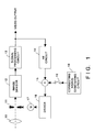
- Fig. 1 is a block diagram illustrating the construction of a backlighting correction circuit.
- Fig. 1 As shown in Fig. 1, light rays from a subject enter via an optical lens 10, the amount of light is limited by an iris 11, and an image is formed on an image sensor 12. A signal resulting from a photoelectric conversion and conforming to the state of the formed image is outputted by the image sensor 12 and converted into a video signal by a signal processing circuit 13, which delivers the video signal as an output.
- the video signal is supplied also to an AE circuit 14, which generates an iris control signal conforming to the video signal.
- a driver 16 Upon receiving the iris control signal from the AE circuit 14 via an adder 15, a driver 16 generates a drive signal which drives an ig meter 17, whereby automatic adjustment of the amount of light by the iris is realized.
- a BLC switch 19 is turned on (closed), whereby a correction signal generating 18 supplies the driver 16 with a signal for widening the opening of the diaphragm. This signal arrives via the adder 15. As a result, the driver 16 drives the ig meter 17 in the opening direction to increase the amount of light incident upon the image sensor 12, whereby the backlighting correction is achieved.
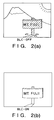
- the image is changed from the BLC-OFF state (the state prior to the backlighting correction), shown in Fig. 2(a), to the BLC-ON state (the state after the backlighting correction), shown in Fig. 2(b).
- the background shows up well in the BLC-OFF state, but the subject is darkened and does not show up very well.
- the tones of the subject are expressed and appear excellently in the BLC-ON state.
- performing the backlighting correction increases the amount of light received by the image sensor, thereby causing the main subject to show up well, but the background appears washed out and cannot be made to appear. This may be understood from Fig. 2(b).
- clipping occurs at a high or low level owing to the limitation upon the dynamic range of the image sensor, so that it is not possible to pick up the images of both the main subject and background well.
- an object of the present invention is to provide an image sensing apparatus having a tone control function in which it is possible to realize excellent exposure of both the main subject and background.
- Another object of the present invention is to provide an image sensing apparatus having a tone control function capable of expressing tones over a wide apparent range.
- Still another object of the present invention is to provide an image sensing apparatus having a tone control function capable of suppressing the occurrence of false color signals.
- a further object of the present invention is to provide an image sensing apparatus having a tone control function in which exposure control can be carried out based upon light information indicative of individual areas in a frame.
- Yet another object of the present invention is to provide an image sensing apparatus having a tone control function in which the state of an imaged picture can be varied by intentionally changing the opening of an iris.
- an image sensing apparatus having a tone-control function, characterized by including sensing means for receiving a light signal, performing a photoelectric conversion and storing information, and control means for changing an amount of electric charge storable by the sensing means, wherein the storable amount of electric charge is changed by the control means during a unit light-storage interval that is for forming one picture.
- the image sensing apparatus having the tone control function of the present invention performs both an operation in which exposure suited to a subject having little luminance is performed by setting the storable amount of electric charge to be small during a unit light-storage interval, and an operation in which exposure suited to a subject having a high luminance is performed by setting the storable amount of electric charge to be large during the unit light-storage interval, these operations being combined to achieve excellent exposure for both a subject with little luminance and a subject with high luminance in one picture.
- an image sensing apparatus having a tone-control function, characterized by including sensing means for receiving a light signal, performing a photoelectric conversion and storing information, and control means for changing an amount of electric charge storable by the sensing means, wherein, during a unit light-storage interval that is for forming one picture, the control means performs control so as to change the storable amount of electric charge in a plurality of steps and set, in dependence upon image information, the timing at which the storable amount of electric charge is changed in the plurality of steps.
- the image sensing apparatus having the tone control function of the present invention performs both an operation in which exposure suited to a subject having little luminance is performed by setting the storable amount of electric charge to be small during a unit light-storage interval, and an operation in which exposure suited to a subject having a high luminance is performed by setting the storable amount of electric charge to be large during the unit light-storage interval, the timing at which these operations are changed over being set in dependence upon the image information to achieve excellent exposure for both a subject with little luminance and a subject with high luminance in one picture.
- an image sensing apparatus having a tone-control function, characterized by including sensing means for receiving a light signal, performing a photoelectric conversion and storing information, and control means for changing an amount of electric charge storable by the sensing means, wherein, during a unit light-storage interval that is for forming one picture, the control means performs control so as to change the storable amount of electric charge in a plurality of steps and set, in dependence upon image information, the levels of the plurality of steps.
- the image sensing apparatus having the tone control function of the present invention performs both an operation in which exposure suited to a subject having little luminance is performed by setting the storable amount of electric charge to be small during a unit light-storage interval, and an operation in which exposure suited to a subject having a high luminance is performed by setting the storable amount of electric charge to be large during the unit light-storage interval, the level of the storable amount of electric charge in each of these operations being set in dependence upon the image information to achieve excellent exposure for both a subject with little luminance and a subject with high luminance in one picture.
- an image sensing apparatus having a tone-control function, characterized by including sensing means for receiving a light signal, performing a photoelectric conversion and storing information, and control means for changing an amount of electric charge storable by the sensing means, wherein, during a unit light-storage interval that is for forming one picture, the control means performs control so as to change the storable amount of electric charge, the mu-factor of a color signal being changed in association with the change in the storable amount of electric charge.
- the image sensing apparatus having the tone control function of the present invention is such that when a high-luminance color signal overflows by exceeding the storable amount of electric charge (which overflow accompanies a change in the storable amount of electric charge), the mu-factor of the color signal is reduced to prevent the occurrence of a false color signal.
- an image sensing apparatus having a tone-control function, characterized by including sensing means for receiving a light signal, performing a photoelectric conversion and storing information, and control means for changing an amount of electric charge storable by the sensing means, wherein, during a unit light-storage interval that is for forming one picture, the control means performs control so as to change the storable amount of electric charge in a plurality of steps and set, for each of the plurality of steps, and on the basis of image information indicative of individual areas in the one picture, the levels of the plurality of steps as well as the timing at which the storable amount of electric charge is changed in the plurality of steps.
- the image sensing apparatus having the tone control function of the present invention performs both an operation in which exposure suited to a subject having little luminance is performed by setting the storable amount of electric charge to be small during a unit light-storage interval, and an operation in which exposure suited to a subject having a high luminance is performed by setting the storable amount of electric charge to be large during the unit light-storage interval.
- exposure operation applied to a low-luminance subject exposure is controlled based upon image information indicative of the low-luminance portion of the subject.
- exposure operation applied to a high-luminance subject exposure is controlled based upon image information indicative of the high-luminance portion of the subject.
- an image sensing apparatus having a tone-control function, characterized by including sensing means for receiving a light signal, performing a photoelectric conversion and storing information, and control means for changing an amount of electric charge storable by the sensing means, wherein, during a unit light-storage interval that is for forming one picture, the control means performs control so as to change the storable amount of electric charge in a plurality of steps and perform storage of electrical charge for prescribed times in distributed fashion in the plurality of steps, thereby controlling substantial exposure time in the plurality of steps.
- the image sensing apparatus having the tone control function of the present invention performs both an operation in which exposure suited to a subject having little luminance is performed by setting the storable amount of electric charge to be small during a unit light-storage interval, and an operation in which exposure suited to a subject having a high luminance is performed by setting the storable amount of electric charge to be large during the unit light-storage interval, these operations being combined to achieve excellent exposure for both a subject with little luminance and a subject with high luminance in one picture.
- the storage of charge for the prescribed time is performed in distributed or dispersed fashion, and substantial exposure time in each operating interval is controlled, thereby making it possible to freely set the iris opening and provide a representation of video over a wide range.
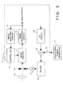
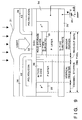
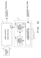
- Fig. 3 is a block diagram illustrating the construction of an embodiment of an image sensing apparatus according to the present invention.
- the lower half of Fig. 3 is identical with the conventional circuit arrangement shown in Fig. 1.
- the concept of this embodiment will now be described based upon Fig. 3.
- the image analyzing circuit 2 performs analysis of luminance information possessed by the video signal and supplies a controller 3 with a luminance histogram, etc.
- a mode changeover switch 5 By changing over a mode changeover switch 5 in dependence of the condition of the subject, either a normal mode (ordinary exposure mode) or BLC-ON mode (backlighting correction mode) is selected as the photographic mode.
- the controller 3 Upon receiving a photographic mode selecting signal from the mode changeover switch 5 and information such as a luminance histogram from the image analyzing circuit 2, the controller 3 controls the drive of the image sensor 1 in dependence upon this information.
- the AE circuit 14 generates an iris control signal in dependence upon the video signal, and applies this signal to the driver 16 via the adder 15.
- the driver 16 Upon receiving the iris control signal, the driver 16 generates a drive signal for driving the ig meter 17, thereby performing an automatic adjustment of the amount of light by the iris.
- a correction signal used in a state such as the backlighted state is generated by a correction signal generating circuit 4.
- the BLC switch 19 is interlocked with the mode changeover switch 5.
- the BLC switch 19 is turned on, i.e., closed.
- the correction signal from the correction signal generating circuit 4 is applied to the adder 15, just as in the case of conventional backlighting correction, thereby shifting the output of the AE circuit 14 in a direction which widens the opening of the iris 11.
- the present embodiment is such that when a backlighted state prevails, iris control similar to that in conventional backlighting correction is carried out to increase the amount of light incident upon the image sensor 1, under which conditions (namely with the BLC switch 19 closed) a prescribed degree of driving control is applied to the image sensor 1 by the controller 3 in an effort to obtain an excellent state of exposure for both the main subject and background, as illustrated in Fig. 4(b).
- the image sensor 1 controlled by the controller 3 will now be described.
- Image sensors are of a large number of types, such as of the CCD-, MOS- and BASIS-type, depending upon the principle of photoelectric conversion adopted.
- a CCD which is used most commonly in video cameras at the present time, will be discussed as one example.
- CCDs are classified according to the structure of the semiconductor device, namely according to the type of charge reading system, such as FT (frame transfer) or FIT (frame interline transfer), and the type of processing for unnecessary charge, such as the processing in a VOD-type CCD, where VOD is the abbreviation of vertical overflow drain.
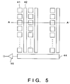
- Fig. 5 is a plan view schematically illustrating the structure of an interline transfer-type (IT-type) CCD.
- Numeral 41 denotes a sensor portion (sensing means) which performs a photoelectric conversion, 42 a vertical transfer register, 44 a horizontal transfer register, and 45 an output amplifier.
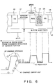
- Fig. 6 is a sectional view taken along line A-A′ of Fig. 2 and a diagram illustrating the states of potentials at various portions corresponding to this cross section.
- numeral 46 denotes a channel stop (CS) for pixel separation, 47 a read-out gate (ROG) for transferring the electric charge, which has accumulated in the sensor portion 41, to the vertical transfer register 42, 48 a substrate, and 49 an oxide film.
- CS channel stop
- ROG read-out gate
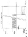
- Fig. 7 is a timing chart of signals in one field interval (e.g., about 1/60 sec according to the NTSC) of a standard television signal.
- a ⁇ ROG pulse is a pulse applied to the read-out gate (ROG) 47. When the logic level of this pulse is "H”, the potential of the read-out gate 47 falls and the electric charge in the sensor portion 41 is transferred to the vertical transfer register 42.
- An elimination pulse ⁇ SUB is a pulse applied to the substrate 48. When this pulse is "H", the electric charge which has accumulated in the sensor portion 41 is swept out (eliminated) to the exterior through a ⁇ SUB terminal.
- the ⁇ ROG pulse is applied during the vertical retrace interval, and the ⁇ SUB pulse is applied during the horizontal retrace interval or in the proximity of the horizontal retrace interval.
- the next field interval begins.
- ⁇ SUB attains the "H" level in the horizontal retrace interval at time t1
- the electric charge which has accumulated from t0 to t1 does not remain in the sensor portion 41.
- ⁇ SUB is at the "L" level from time t1 to time t2, electric charge is stored in the sensor portion 41 during this time period.
- This charge is transferred to the vertical transfer register 2 by the "H"-level ⁇ ROG pulse applied at time t2.
- the end result is that the exposure time in this case becomes (t2-t1).
- Fig. 8 is a plan view schematically showing the structure of a a frame interline transfer-type (FIT-type) CCD.
- This CCD differs from the interliie transfer-type (IT-type) CCD shown in Fig. 5 in that a memory 63 is provided.
- the number of memory cells in the memory 63 is the same as the number of cells of the sensor portions (sensing means) 61.
- the charge from the sensor portion 61 migrates to the vertical transfer register 62, after which it is transferred to the memory 63 in the vertical retrace interval. Thereafter, the charge is transferred to the horizontal transfer register 64, whence it is read out through the output amplifier 65.
- a photodiode (PD) of a sensor portion 33 via an oxide layer (SiO2) 32 and a hole-storage layer for reducing dark current.
- Unnecessary light is prevented from impinging upon portions other than the sensor portion by an aluminum layer (Al) 36 acting as a shield. Owing to this shutting out of incident light, the light-receiving area of the CCD cannot be utilized effectively and the aperture efficiency declines.
- a condensing lens 31 for the purpose of compensating for this decline in aperture efficeincy is provided for each pixel.
- V-CCD vertical transfer register
- Each pixel is provided with channel stopper 39 which separates the charge produced by each pixel, thereby preventing the charges from mixing.
- a P layer 34 underlies the sensor portion 33, and an N-S layer underlies the P layer 34. Discharging of unnecessary charge is performed by a substrate bias potential V sub 30 developed across these two layers.
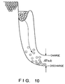
- Fig. 10 is a diagram illustrating the charge elimination operation of the VOD-type CCD in terms of a change in state of potential.
- the line indicated by “CHARGE” is a potential diagram indicative of storage of photoelectric charge
- the line indicated by DISCHARGE” is a potential diagram indicative of elimination of unnecessary charge.
- CHARGE electric charge accumulates in the depression at the top of the diagram.
- DISCHARGE ⁇ Vsub is superimposed upon the substrate voltage V sub , producing V sub + ⁇ V sub which causes the depression to vanish, as a result of which the accumulated charge is cast out toward the bottom of the diagram.
- the P layer is disposed below the layer of the N-type V-CCD in order to prevent unnecessary charge having a long recombination time from penetrating from below and mixing with charge in the vertical transfer register 38 as noise at the time of unnecessary charge elimination.
- Fig. 11 is a timing chart showing a change in the potential V sub at operation of the above-described high-speed shutter.
- the V sub potential is varied in pulsed fashion at a predetermined time interval, as shown in (c) of Fig. 11, so that the elimination of the unnecessary charge stored in the sensor portion 61 is repeated until a prescribed time.
- storage of photoelectric charge is performed for a time t in the latter half of one field interval (one picture), and the stored charge indicated by "HIGH” is read out as image information by a read-out pulse shown in (b) of Fig. 11.
- a high-speed shutter effect for carrying out storage for time t is obtained.
- the difference in the manner of charge storage is illustrated in Fig. 11(a), in which "NORMAL" indicates operation at the time of ordinary storage and "HIGH” indicates storage at the time of the high-speed shutter operation.
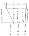
- Fig. 12 illustrates the manner in which plural levels of the Vsub potential are set and control is performed selectively. In comparison with LEVEL 1, the potential depression is set to be deeper at LEVEL 2, whereby a larger amount of electric charge is capable of being stored than at LEVEL 1.
- the ease of charge overflow is controlled by controlling the V sub potential, with the black circles in Fig. 12 occupying the difference between the two levels.
- the storable amount of charge is that indicated by the white circles at LEVEL 1.
- the storable amount of charge is the total of charge indicated by the black circles, namely the total of both the white and black circles.
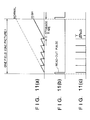
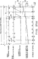
- Fig. 13 is a timing chart showing an example in which the above-described control of V sub is performed and a changeover is made between the state of LEVEl 1 and the state of LEVEL 2 at a prescribed timing in one picture.
- charge which exceeds the saturated charge level 1 overflows and clipping occurs at the high-luminance portion, as illustrated by the characteristic of the flat portion indicated by the solid line in Fig. 13(a), within the initial time period t1 in one picture.
- the saturated charge level 1 is 100%, for example, light from the subject having a luminance in excess of this value is clipped in its entirety.
- control is changed over in the latter half of one picture, the V sub potential is placed in the LEVEL 2 state and the saturated charge level also is raised to 2 to provide sum extra margin for storage, in which state storage of the photoelectric charge is continued for time t2 .
- t1 + t2 1/60 sec for the NTSC television signal
- t2 is the suitable exposure for a subject having a luminance three stops higher than a subject whose suitable exposure is t1.
- a picture corresponding to the BLC-ON state (the backlighting correction state) of the prior-art example is imaged during time t1 , the appropriate exposure is achieved for the main subject and the background is clipped owing to its high luminance.
- a picture corresponding to the BLC-OFF state (the state in which no compensation is made for backlighting ) of the prior-art example is imaged, the appropriate exposure is achieved for the background portion, which is three stops brighter than the main subject, and the main subject almost fails to appear.
- the charge accumulated during time t1 and the charge accumulated during time t2 are added by the photoelectric storage portion of each pixel, and a picture of the kind shown in Fig. 4(b) is obtained as a result.
- Fig. 14 illustrates an example of the construction of the controller 3 described in Fig. 3.
- the controller 3 is supplied with, e.g., information indicative of a luminance histogram from the image analyzing circuit 2, and controls the drive of the image sensor 1 in conformity with the mode selected by the mode changeover switch 5.
- a control-mode changeover unit 301 Upon receiving the selection signal from the mode changeover switch 5, a control-mode changeover unit 301 sets the driving mode of the controller 3 to either the NORMAL mode (ordinary photographic mode) or BLC-ON mode (backlighting correction mode).
- the V sub potential (the substrate voltage value) is set to the state shown at LEVEL 2 in Fig. 12 so as to attain the maximum value of the saturated charge level decided by the performance of the image sensor 1 per se.
- V sub is changed over between LEVEL 1 and LEVEL 2 in Fig. 12 in the course of photographing one picture.
- the setting of the changeover timings (t1 and t2 ) and the setting of the saturated charge level of LEVEL 1 are performed respectively by a timing control circuit 303 and a level control circuit 302 based upon the results of image analysis of the aforementioned luminance histogram or the like.
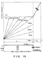
- the overall photoelectric conversion characteristic which varies depending upon the settings of the level and timing is non-linear, as depicted in Fig. 15.
- the manner in which the characteristic changes depending upon the level setting is indicated by the white arrows, and the manner in which the characteristic changes depending upon the timing setting is indicated by the black arrows.
- the automatic exposure adjusting mechanism of a video camera or the like ordinarily controls an iris or the like in such a manner that the integrated value of one picture of a luminance signal will approach a predetermined value.
- the iris 11 is controlled in the same manner in a case where the integrated value of one picture of a luminance signal is the same even if the distribution of brightness in one picture differs, as indicated by the curves a and b of the luminance histogram shown in Fig. 16(a).
- the curve a is a distribution pattern, which is readily produced at the time of backlighted photography, indicative of the occurrence frequency of luminance
- the curve b is a distribution pattern, which is readily produced at the time of frontlighted photography, indicative of the occurrence frequency of luminance.
- the BLC switch 19 When the BLC-ON mode (the backlighting correction mode) is selected by the mode changeover switch 5 in order to compensate for backlighting, the BLC switch 19 is closed and a transition is made from the curve a to the curve c shown in Fig. 16(b). Since the base of the image pick-up signal for which darkening of the subject would occur is raised and made to approach the aforementioned predetermined value (indicated by the one-dot chain line) serving as the criterion for appropriate exposure, the image pick-up signal of the bright portion causes high-luminance clamping and, in terms of the occurrence frequency, the pattern becomes one shifted toward the bright portion.
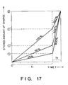
- Fig. 17 illustrates the relationship between storage time t (plotted along the horizontal axis) at various intensities (25%, 50%, 100%) of incident light and amount of stored charge (plotted along the vertical axis) in a case where potential level is changed to set three charge saturation levels indicating ease of photoelectric charge overflow.
- the one-dot chain line 1-a is the characteristic which prevails when the incident light intensity is 25%
- the dashed line 1-b is the characteristic which prevails when the incident light intensity is 800%.
- the characteristic obtained by combining these two characteristics is the solid line 1.
- An appropriate photoelectric conversion can be carried out by controlling the setting of potential level by a video signal resulting from image pick-up.
- Figs. 19(a) and (b) illustrate conceptual diagrams of an example in which a video signal is subjected to histogram analysis by the image analyzing circuit 2.
- Fig. 19(a) illustrates the distribution of the occurrence frequency of luminance level Y
- Fig. 19 (b) illustrates a graph of the cumulative frequency thereof.
- Various methods of correlating the above-described potential-level setting and imaged picture are conceivable, and each has its own advantages. One example of such a method will be described here.
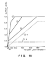
- the dashed line (a) in Figs. 19(a) and 19(b) indicates that the occurrence frequency concentrates in the dark portion, and that the bright portion concentrates at the MAX level believed to be clipped. In such case, it is appropriate to set the potential level at level 1 in Fig. 17 and strength the compression effect of the luminance difference in one picture.
- the solid line (b) in Figs. 19(a) and 19(b) is the occurrence frequency of the bright portion which concentrates at the intermediate-luminance level and does not produce excessive clipping. In this case, as opposed to the above, it is appropriate to set the potential level at level 1 ′ in Fig. 17 and comparatively reduce compression of the luminance difference to make half-tone reproduction easier.
- a judgment of this kind can be achieved by providing the cumulative frequency of Fig. 19(b) with a threshold value (solid line c) and effecting a division into classes (the three areas 1, 1 ′, 1 ⁇ indicated by the one-dot chain lines) at the luminance levels which prevail when the cumulative frequency reaches 50%, by way of example.
- a threshold value solid line c
- Fig. 20 is a diagram showing the construction of a color video camera using a single-plate color filter
- a distribution amplifier 145 distributes information relating to contrast to luminance-signal processing circuit 146 and color information to a color-signal processing circuit 147. In other words, the amplifier 145 outputs so-called Y- and C-signals.
- a gain control-signal generating circuit 148 generates a control signal for realizing a gain characteristic of the kind shown in Fig. 21(b) in order that a variable gain amplifier 149 will reduce the mu-factor of a color signal having a luminance level which exceeds a threshold value TH2 shown in Fig. 21(a). Thereafter, the luminance and color signals are mixed by a mixer 140 and outputted as a composite TV signal.
- a plurality of saturation charge levels of pixels are set in one picture, and therefore it is necessary to set correspondingly a plurality of points at which the color-signal mu factor is reduced.
- Fig. 22 is a block diagram showing only the portion of circuitry dealing with color signals. As in the case of Fig. 20, Y and C signals are outputted. These signals enter a threshold-value generating circuit 160, which generates a plurality of threshold values corresponding to the pixel saturation charge levels and applies these threshold values to a gain-control signal generating circuit 161.
- Figs. 23(a), (b) respectively illustrate the relationship between these saturation charge levels (1, 2) and threshold values (TH1, TH2, TH3) and the relationship between the threshold values and gain characteristic.
- a window comparator mode is adopted and therefore two threshold values (TH1, TH2) are set with respect to one level. Gain is reduced between these two threshold values. This makes it possible to suppress a false color signal at an intermediate luminance level in the imaged picture. A false color signal at a high luminance can be suppressed by the threshold value TH3 in the same manner as in the case of Fig. 21(a) and 21(b).
- a method of performing exposure control (the aforementioned iris control) for low-luminance area video and a method of performing exposure control (the aforementioned setting of time period t2 ) for high-luminance area video based upon image information of the entirety of one picture have been described above.
- a method will now be described in which video signals cut from individual areas of one picture are used in each of these two types of exposure control.
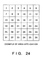
- Fig. 24 illustrates an example in which an image is divided into a plurality of areas.
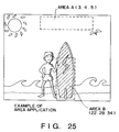
- An example in which these 36 image subdivisions are applied at the time of backlighted photography is shown in Fig. 25.
- an area A (3, 4, 5) is selected as a typical area from a high-luminance portion
- an area B (22, 28, 34)) is selected as a typical area from a low-luminance portion.
- the areas A and B each have identical numbers of blocks (three blocks each) in this example. However, in a case where the numbers of blocks differ, it will suffice to supplement these with weighting coefficients.
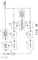
- Fig. 26 illustrates a specific example of a circuit arrangement for exposure control based upon image division.
- the signal resulting from image pick-up is analyzed by the image analyzing circuit 2, such as the aforementioned luminance histogram analyzing means, and several blocks of areas having a high occurrence frequency of high and low luminances are selected starting from the higher order blocks.
- the gate signal generating circuit 161 Based upon the video signals indicative of these areas of several blocks, a gate signal generating circuit 161 generates a control signal for controlling the ON/OFF action of a gate a 162 and a gate b 163 corresponding to the areas A and B, respectively.
- Exposure control circuits AE a 164, AE b 165 generate control signals for drivers 166, 16 using the video signals selected by the above-mentioned gates.
- AE a 164 is for setting t2 and therefore is an AE based upon a shutter speed for a high-luminance area.
- AE a 165 is an AE based upon an iris for a low-luminance area. This is just a simple example and there are various other AE methods. These know methods can be utilized in control of each of the areas.
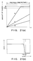
- Fig. 27(a) illustrates an example of an exposure operation when using a manual iris.
- storage of photoelectric charge for low luminance is performed continuously for time t1 , with the saturated charge level of the sensor portion being 1 .
- the sensor portion which receives the light from the high-luminance portion (background) of the picture develops overflow at the initial stage of time t1, as illustrated.
- ⁇ ROG transfer pulses and ⁇ SUB elimination pulses are driven in the manner illustrated in a state where the saturated charge level has been set high over time t2 in the latter part of one picture, thereby performing storage for a storage time t3 in a dispersed manner (a multiple-exposure operation by an FIT-type CCD) and carrying out storage of photoelectric charge for high luminance.
- This multiple-exposure operation by an FIT-CCD refers to performing storage of photoelectric charge in dispersed fashion within a predetermined period of time.
- the manner in which the saturated charge level of the sensor portion changes is indicated by the two-dot chain line.
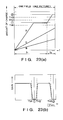
- Figs. 27(b), (c) Two examples shown in Figs. 27(b), (c) are illustrated as exposure states to be set anew.
- Fig. 27(b) low-luminance exposure is arranged at the very beginning of the picture, light is stored continuously for 1/4 the time, and high-luminance storage is dispersed evenly in the remaining portion of the picture.
- Fig. 27(a) there are 12 storage intervals (b1 , b2, ..., b12).
- Figs. 27(b) and (c) there are three storage intervals (b1 , b2 , b3 ), namely 1/4.
- Fig. 27(c) it is arranged so that the total light storage time for low-luminance exposure becomes 1/4 and is dispersed over the beginning portion of the picture. Storage inclusive of the light storage pulses for high-luminance is evenly dispersed in one picture.
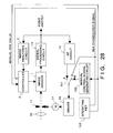
- Fig. 28 is a block diagram illustrating an example of an arrangement for realizing a manual iris operation.
- a manual (M) or automatic (A) iris is selected by an operating key 153, thereby producing an M/A changeover signal which changes over the contact of an iris control-signal changeover switch 151 to the M side.
- the changeover signal is simultaneously supplied to the controller 3, which is the CCD control circuit.
- the controller 3 Since the manual iris value also is transmitted to the controller 3, the latter calculates the factor by which the quantity of light will change and executes compression processing for compressing the storage interval by the above-described multiple-exposure operation.
- the driver 16 Since the manual iris value is sent to a manual control-signal generating circuit 152, the driver 16 is instructed of a new set value for the iris by changeover of the switch 151, and the iris 11 is driven via the ig meter 17 to obtain a prescribed depth of field. Thus the image pick-up optical lens between the lens 10 and image sensor 1 is changed.
- the saturated charge level of the sensor portion in the latter part of one picture is made higher than in the earlier part of the picture in order to make it more difficult for the photoelectric charge to overflow.
- an image of a high-luminance portion which is clipped in the prior art and could not be reproduced is capable of being reproduced according to this invention.
- VOD-type CCD which is presently the most widely used
- simple control processing circuitry a backlighting correction, which has been a major problem when performing photography with a video camera, can be carried out in an effective manner.
- t1 , t2 are interrelated and control is performed in dependence upon the image information. Therefore, in a case where the luminance difference in one picture is small, high-luminance storage time t2 is lengthened and t1 is shortened correspondingly. However, in imaging a low-luminance portion, a photoelectric conversion time equivalent to that of ordinary photography is assured as long as overflow does not occur. As a result, a deterioration in the S/N ratio of the low-luminance portion does not readily occur.
- the potential level of LEVEL 1 is set so as to facilitate overflow. This makes finer tone representation possible regardless of automatic or manual operation.
- the tones of the background can be expressed and an automatic exposure adjusting function can be exploited to make possible a video representation over a wide range.
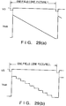
- a method has been described in which the potential of V sub is changed over between two levels, namely LEVEL 1 and LEVEL 2, in the foregoing embodiment.
- Fig. 29(b) an arrangement may be adopted in which the potential of V sub and the changeover time are divided finely into steps so that the changeover is made stepwise in one picture.
- a sweep-like operation as shown in Fig. 29(a) can be adopted, in which the potential of V sub and the changeover time are varied continuously.
- the essential concept of one aspect of the present invention is that the clipping level for a light detection signal is different for different portions ofan exposure interval.
- the light detection signal obtained over a first portion of an exposure interval is clipped for light having an intensity greater than a preset level
- the light detection signal obtained over a second portion of the exposure interval is not clipped for at least some light intensities greater than the preset level.
- Both portions of the exposure interval may be made up of a plurality of separate sub-portions.
- the first portion can be used to allow different light intensities below the preset level to provide different signal levels
- the second portion can be used to allow different light intensities above the preset level to provide different signal levels
- signals obtained in both portions may be used in providing an image signal.
- the clipping may take place in a region in which charges accumulate in response to incident light, or may take place in another part of the apparatus such as a signal storage region. Signals may be read a plurality of times during the exposure interval from a region in which charges accumulate in response to incident light.
Landscapes
- Engineering & Computer Science (AREA)
- Multimedia (AREA)
- Signal Processing (AREA)
- Transforming Light Signals Into Electric Signals (AREA)
Applications Claiming Priority (12)
| Application Number | Priority Date | Filing Date | Title |
|---|---|---|---|
| JP293669/90 | 1990-11-01 | ||
| JP2293670A JP2695521B2 (ja) | 1990-11-01 | 1990-11-01 | 階調制御機能を有する撮像装置 |
| JP293673/90 | 1990-11-01 | ||
| JP293671/90 | 1990-11-01 | ||
| JP2293671A JP2751126B2 (ja) | 1990-11-01 | 1990-11-01 | 階調制御機能を有する撮像装置 |
| JP293670/90 | 1990-11-01 | ||
| JP2293669A JP2714248B2 (ja) | 1990-11-01 | 1990-11-01 | 階調制御機能を有する撮像装置 |
| JP293672/90 | 1990-11-01 | ||
| JP2293672A JP2647550B2 (ja) | 1990-11-01 | 1990-11-01 | 階調制御機能を有する撮像装置 |
| JP2293668A JPH04168886A (ja) | 1990-11-01 | 1990-11-01 | 階調制御機能を有する撮像装置 |
| JP2293673A JP2695522B2 (ja) | 1990-11-01 | 1990-11-01 | 撮像装置。 |
| JP293668/90 | 1990-11-01 |
Publications (3)
| Publication Number | Publication Date |
|---|---|
| EP0484135A2 true EP0484135A2 (de) | 1992-05-06 |
| EP0484135A3 EP0484135A3 (en) | 1992-09-23 |
| EP0484135B1 EP0484135B1 (de) | 1996-09-04 |
Family
ID=27554484
Family Applications (1)
| Application Number | Title | Priority Date | Filing Date |
|---|---|---|---|
| EP91310028A Expired - Lifetime EP0484135B1 (de) | 1990-11-01 | 1991-10-30 | Bildabtastungsvorrichtung mit Tonsteuerfunktion |
Country Status (3)
| Country | Link |
|---|---|
| US (2) | US5295001A (de) |
| EP (1) | EP0484135B1 (de) |
| DE (1) | DE69121838T2 (de) |
Cited By (3)
| Publication number | Priority date | Publication date | Assignee | Title |
|---|---|---|---|---|
| EP0700204A3 (de) * | 1994-08-31 | 1996-12-04 | Matsushita Electric Industrial Co Ltd | Bildaufnahmevorrichtung mit weitem Dynamikbereich |
| EP0991128A3 (de) * | 1998-09-25 | 2004-02-04 | Lockheed Martin Corporation | Erweiterung des Dynamikbereichs von CCD-Bildaufnahmevorrichtungen |
| EP1814319A1 (de) * | 2006-01-31 | 2007-08-01 | Sony Corporation | Abbildungsvorrichtung, Steuerungverfahren der Abbildungsvorrichtung, Programm für Steuerungsverfahren der Abbildungsvorrichtung, Aufzeichnungsmedium mit darauf aufgezeichnetem Programm für Steuerungsverfahren der Abbildungsvorrichtung |
Families Citing this family (21)
| Publication number | Priority date | Publication date | Assignee | Title |
|---|---|---|---|---|
| KR0149737B1 (ko) * | 1993-07-20 | 1998-10-15 | 사토 후미오 | 고체촬상장치 |
| US5666569A (en) * | 1994-08-25 | 1997-09-09 | Flashpoint Technology, Inc. | System and method for detecting and indicating proper focal distance in a fixed lens camera |
| US6292212B1 (en) * | 1994-12-23 | 2001-09-18 | Eastman Kodak Company | Electronic color infrared camera |
| US6160579A (en) | 1995-08-01 | 2000-12-12 | Canon Kabushiki Kaisha | Image processing apparatus and method |
| US5614948A (en) * | 1996-04-26 | 1997-03-25 | Intel Corporation | Camera having an adaptive gain control |
| JP3873157B2 (ja) * | 1997-11-13 | 2007-01-24 | カシオ計算機株式会社 | 電子カメラ装置および撮像方法 |
| JP3969836B2 (ja) * | 1998-04-24 | 2007-09-05 | キヤノン株式会社 | 信号処理装置および撮像用信号処理方法 |
| US6657663B2 (en) * | 1998-05-06 | 2003-12-02 | Intel Corporation | Pre-subtracting architecture for enabling multiple spectrum image sensing |
| US6747696B1 (en) * | 1999-03-26 | 2004-06-08 | Casio Computer Co., Ltd. | Camera capable of canceling noise in image data and signal processing method thereof |
| US6947089B1 (en) * | 1999-05-14 | 2005-09-20 | Canon Kabushiki Kaisha | Image pickup apparatus |
| US20010007475A1 (en) * | 2000-01-06 | 2001-07-12 | Asahi Kogaku Kogyo Kabushiki Kaisha | Image pickup device and its mounting structure for an optical low-pass filter |
| US20020154242A1 (en) * | 2001-04-24 | 2002-10-24 | Robins Mark N. | Method and apparatus for generating multiple exposures in a digital camera |
| JP3981034B2 (ja) * | 2003-03-25 | 2007-09-26 | 富士フイルム株式会社 | カラー画像取得装置およびカラー電子カメラ |
| US7362361B2 (en) * | 2003-11-28 | 2008-04-22 | Victor Compay Of Japan, Ltd. | Noise suppressing circuit using luminance detection |
| KR100609155B1 (ko) * | 2004-03-22 | 2006-08-02 | 엘지전자 주식회사 | 영상 처리 장치 및 이를 이용한 역광 보정 방법 |
| US20050212936A1 (en) * | 2004-03-25 | 2005-09-29 | Eastman Kodak Company | Extended dynamic range image sensor with fixed pattern noise reduction |
| US20060082670A1 (en) * | 2004-10-14 | 2006-04-20 | Eastman Kodak Company | Interline CCD for still and video photography with extended dynamic range |
| JP4388909B2 (ja) * | 2005-04-25 | 2009-12-24 | イーストマン コダック カンパニー | 画素欠陥補正装置 |
| US7894686B2 (en) * | 2006-01-05 | 2011-02-22 | Lsi Corporation | Adaptive video enhancement gain control |
| JP2007251343A (ja) * | 2006-03-14 | 2007-09-27 | Pentax Corp | 撮像素子駆動装置及びオートフォーカスユニット |
| JP5600405B2 (ja) | 2009-08-17 | 2014-10-01 | キヤノン株式会社 | 画像処理装置、画像処理方法及びプログラム |
Family Cites Families (9)
| Publication number | Priority date | Publication date | Assignee | Title |
|---|---|---|---|---|
| US3953733A (en) * | 1975-05-21 | 1976-04-27 | Rca Corporation | Method of operating imagers |
| US4479062A (en) * | 1981-02-06 | 1984-10-23 | Asahi Kogaku Kogyo Kabushiki Kaisha | Photo-electric conversion device with accumulation time control |
| US4635126A (en) * | 1981-12-18 | 1987-01-06 | Canon Kabushiki Kaisha | Image pick-up system |
| JPS5932265A (ja) * | 1982-08-18 | 1984-02-21 | Toshiba Corp | イメージセンサの駆動方法 |
| JPS6020687A (ja) * | 1983-07-15 | 1985-02-01 | Nippon Kogaku Kk <Nikon> | 電子スチルカメラ |
| JPS6074878A (ja) * | 1983-09-30 | 1985-04-27 | Canon Inc | 光電変換器の蓄積時間補正装置 |
| JPS61274475A (ja) * | 1985-05-29 | 1986-12-04 | Toshiba Corp | 電子スチルカメラ |
| US4901152A (en) * | 1987-08-31 | 1990-02-13 | Canon Kabushiki Kaisha | Image pickup apparatus |
| US5182658A (en) * | 1988-07-27 | 1993-01-26 | Canon Kabushiki Kaisha | Image pickup apparatus for controlling accumulation time in photoelectric elements |
-
1991
- 1991-10-28 US US07/783,354 patent/US5295001A/en not_active Expired - Lifetime
- 1991-10-30 EP EP91310028A patent/EP0484135B1/de not_active Expired - Lifetime
- 1991-10-30 DE DE69121838T patent/DE69121838T2/de not_active Expired - Lifetime
-
1994
- 1994-03-04 US US08/205,390 patent/US5406391A/en not_active Expired - Lifetime
Cited By (3)
| Publication number | Priority date | Publication date | Assignee | Title |
|---|---|---|---|---|
| EP0700204A3 (de) * | 1994-08-31 | 1996-12-04 | Matsushita Electric Industrial Co Ltd | Bildaufnahmevorrichtung mit weitem Dynamikbereich |
| EP0991128A3 (de) * | 1998-09-25 | 2004-02-04 | Lockheed Martin Corporation | Erweiterung des Dynamikbereichs von CCD-Bildaufnahmevorrichtungen |
| EP1814319A1 (de) * | 2006-01-31 | 2007-08-01 | Sony Corporation | Abbildungsvorrichtung, Steuerungverfahren der Abbildungsvorrichtung, Programm für Steuerungsverfahren der Abbildungsvorrichtung, Aufzeichnungsmedium mit darauf aufgezeichnetem Programm für Steuerungsverfahren der Abbildungsvorrichtung |
Also Published As
| Publication number | Publication date |
|---|---|
| DE69121838D1 (de) | 1996-10-10 |
| US5295001A (en) | 1994-03-15 |
| US5406391A (en) | 1995-04-11 |
| EP0484135A3 (en) | 1992-09-23 |
| DE69121838T2 (de) | 1997-01-30 |
| EP0484135B1 (de) | 1996-09-04 |
Similar Documents
| Publication | Publication Date | Title |
|---|---|---|
| EP0484135B1 (de) | Bildabtastungsvorrichtung mit Tonsteuerfunktion | |
| US6480226B1 (en) | Image pickup apparatus having gradation control function for providing image signals definitive of backlighted objects | |
| US6630960B2 (en) | Image pickup device | |
| EP0528433B1 (de) | Videokamera mit einer Mehrzahl von photographischen Betriebsarten | |
| US4901152A (en) | Image pickup apparatus | |
| JP3297485B2 (ja) | 撮像装置 | |
| JP3551568B2 (ja) | 撮像装置 | |
| JP2872833B2 (ja) | ビデオカメラ | |
| JPH0564062A (ja) | 撮像装置 | |
| JP2714248B2 (ja) | 階調制御機能を有する撮像装置 | |
| JP2751126B2 (ja) | 階調制御機能を有する撮像装置 | |
| JP3402617B2 (ja) | 撮像装置及び撮像方法 | |
| JP3244727B2 (ja) | 撮像装置及び撮像方法 | |
| JP2695522B2 (ja) | 撮像装置。 | |
| JP2695521B2 (ja) | 階調制御機能を有する撮像装置 | |
| JPH0556341A (ja) | 撮像装置 | |
| JPH1023324A (ja) | 撮像装置 | |
| JPH0556331A (ja) | 撮像装置 | |
| JP3262348B2 (ja) | 撮像装置及び撮像方法 | |
| JPH0556338A (ja) | 撮像装置 | |
| JP3402616B2 (ja) | 撮像装置及び撮像方法 | |
| JP2647550B2 (ja) | 階調制御機能を有する撮像装置 | |
| JPH0564059A (ja) | 撮像装置 | |
| JPH0556342A (ja) | 撮像装置 | |
| JPH04168886A (ja) | 階調制御機能を有する撮像装置 |
Legal Events
| Date | Code | Title | Description |
|---|---|---|---|
| PUAI | Public reference made under article 153(3) epc to a published international application that has entered the european phase |
Free format text: ORIGINAL CODE: 0009012 |
|
| AK | Designated contracting states |
Kind code of ref document: A2 Designated state(s): DE ES FR GB IT NL |
|
| PUAL | Search report despatched |
Free format text: ORIGINAL CODE: 0009013 |
|
| AK | Designated contracting states |
Kind code of ref document: A3 Designated state(s): DE ES FR GB IT NL |
|
| 17P | Request for examination filed |
Effective date: 19930208 |
|
| 17Q | First examination report despatched |
Effective date: 19950202 |
|
| GRAH | Despatch of communication of intention to grant a patent |
Free format text: ORIGINAL CODE: EPIDOS IGRA |
|
| GRAH | Despatch of communication of intention to grant a patent |
Free format text: ORIGINAL CODE: EPIDOS IGRA |
|
| GRAA | (expected) grant |
Free format text: ORIGINAL CODE: 0009210 |
|
| AK | Designated contracting states |
Kind code of ref document: B1 Designated state(s): DE ES FR GB IT NL |
|
| PG25 | Lapsed in a contracting state [announced via postgrant information from national office to epo] |
Ref country code: IT Free format text: LAPSE BECAUSE OF FAILURE TO SUBMIT A TRANSLATION OF THE DESCRIPTION OR TO PAY THE FEE WITHIN THE PRE;WARNING: LAPSES OF ITALIAN PATENTS WITH EFFECTIVE DATE BEFORE 2007 MAY HAVE OCCURRED AT ANY TIME BEFORE 2007. THE CORRECT EFFECTIVE DATE MAY BE DIFFERENT FROM THE ONE RECORDED.SCRIBED TIME-LIMIT Effective date: 19960904 Ref country code: ES Free format text: THE PATENT HAS BEEN ANNULLED BY A DECISION OF A NATIONAL AUTHORITY Effective date: 19960904 Ref country code: NL Free format text: LAPSE BECAUSE OF FAILURE TO SUBMIT A TRANSLATION OF THE DESCRIPTION OR TO PAY THE FEE WITHIN THE PRESCRIBED TIME-LIMIT Effective date: 19960904 |
|
| REF | Corresponds to: |
Ref document number: 69121838 Country of ref document: DE Date of ref document: 19961010 |
|
| ET | Fr: translation filed | ||
| ET | Fr: translation filed | ||
| NLV1 | Nl: lapsed or annulled due to failure to fulfill the requirements of art. 29p and 29m of the patents act | ||
| PLBE | No opposition filed within time limit |
Free format text: ORIGINAL CODE: 0009261 |
|
| STAA | Information on the status of an ep patent application or granted ep patent |
Free format text: STATUS: NO OPPOSITION FILED WITHIN TIME LIMIT |
|
| 26N | No opposition filed | ||
| REG | Reference to a national code |
Ref country code: GB Ref legal event code: IF02 |
|
| PGFP | Annual fee paid to national office [announced via postgrant information from national office to epo] |
Ref country code: DE Payment date: 20091031 Year of fee payment: 19 |
|
| PGFP | Annual fee paid to national office [announced via postgrant information from national office to epo] |
Ref country code: GB Payment date: 20091028 Year of fee payment: 19 Ref country code: FR Payment date: 20091030 Year of fee payment: 19 |
|
| GBPC | Gb: european patent ceased through non-payment of renewal fee |
Effective date: 20101030 |
|
| PG25 | Lapsed in a contracting state [announced via postgrant information from national office to epo] |
Ref country code: FR Free format text: LAPSE BECAUSE OF NON-PAYMENT OF DUE FEES Effective date: 20101102 |
|
| REG | Reference to a national code |
Ref country code: FR Ref legal event code: ST Effective date: 20110630 |
|
| REG | Reference to a national code |
Ref country code: DE Ref legal event code: R119 Ref document number: 69121838 Country of ref document: DE Effective date: 20110502 |
|
| PG25 | Lapsed in a contracting state [announced via postgrant information from national office to epo] |
Ref country code: GB Free format text: LAPSE BECAUSE OF NON-PAYMENT OF DUE FEES Effective date: 20101030 |
|
| PG25 | Lapsed in a contracting state [announced via postgrant information from national office to epo] |
Ref country code: DE Free format text: LAPSE BECAUSE OF NON-PAYMENT OF DUE FEES Effective date: 20110502 |