EP0481499A2 - Aufnahme/Wiedergabegerät zum Beispiel Speichergerät - Google Patents
Aufnahme/Wiedergabegerät zum Beispiel Speichergerät Download PDFInfo
- Publication number
- EP0481499A2 EP0481499A2 EP91117767A EP91117767A EP0481499A2 EP 0481499 A2 EP0481499 A2 EP 0481499A2 EP 91117767 A EP91117767 A EP 91117767A EP 91117767 A EP91117767 A EP 91117767A EP 0481499 A2 EP0481499 A2 EP 0481499A2
- Authority
- EP
- European Patent Office
- Prior art keywords
- base
- recording medium
- substrate
- probe
- recording
- Prior art date
- Legal status (The legal status is an assumption and is not a legal conclusion. Google has not performed a legal analysis and makes no representation as to the accuracy of the status listed.)
- Granted
Links
- 239000000523 sample Substances 0.000 claims abstract description 85
- 239000000758 substrate Substances 0.000 claims abstract description 38
- 239000000463 material Substances 0.000 claims description 17
- 229910052710 silicon Inorganic materials 0.000 claims description 8
- 229910052732 germanium Inorganic materials 0.000 claims description 4
- 229920001721 polyimide Polymers 0.000 claims description 3
- 229920006254 polymer film Polymers 0.000 claims 5
- 239000004576 sand Substances 0.000 claims 1
- 238000000034 method Methods 0.000 description 15
- XUIMIQQOPSSXEZ-UHFFFAOYSA-N Silicon Chemical compound [Si] XUIMIQQOPSSXEZ-UHFFFAOYSA-N 0.000 description 5
- 238000010276 construction Methods 0.000 description 5
- 238000002474 experimental method Methods 0.000 description 5
- 239000010703 silicon Substances 0.000 description 5
- 229910052581 Si3N4 Inorganic materials 0.000 description 4
- 230000001154 acute effect Effects 0.000 description 2
- 238000010586 diagram Methods 0.000 description 2
- 230000000694 effects Effects 0.000 description 2
- 238000004519 manufacturing process Methods 0.000 description 2
- 239000000126 substance Substances 0.000 description 2
- OKTJSMMVPCPJKN-UHFFFAOYSA-N Carbon Chemical compound [C] OKTJSMMVPCPJKN-UHFFFAOYSA-N 0.000 description 1
- 239000004642 Polyimide Substances 0.000 description 1
- 241000256247 Spodoptera exigua Species 0.000 description 1
- 230000015572 biosynthetic process Effects 0.000 description 1
- 229910052799 carbon Inorganic materials 0.000 description 1
- 239000013078 crystal Substances 0.000 description 1
- 230000001186 cumulative effect Effects 0.000 description 1
- 230000003247 decreasing effect Effects 0.000 description 1
- 238000001514 detection method Methods 0.000 description 1
- 238000011161 development Methods 0.000 description 1
- 238000006073 displacement reaction Methods 0.000 description 1
- ANSXAPJVJOKRDJ-UHFFFAOYSA-N furo[3,4-f][2]benzofuran-1,3,5,7-tetrone Chemical compound C1=C2C(=O)OC(=O)C2=CC2=C1C(=O)OC2=O ANSXAPJVJOKRDJ-UHFFFAOYSA-N 0.000 description 1
- GNPVGFCGXDBREM-UHFFFAOYSA-N germanium atom Chemical compound [Ge] GNPVGFCGXDBREM-UHFFFAOYSA-N 0.000 description 1
- 229910002804 graphite Inorganic materials 0.000 description 1
- 239000010439 graphite Substances 0.000 description 1
- ZHDTXTDHBRADLM-UHFFFAOYSA-N hydron;2,3,4,5-tetrahydropyridin-6-amine;chloride Chemical compound Cl.NC1=NCCCC1 ZHDTXTDHBRADLM-UHFFFAOYSA-N 0.000 description 1
- 238000005259 measurement Methods 0.000 description 1
- 230000003446 memory effect Effects 0.000 description 1
- 238000005459 micromachining Methods 0.000 description 1
- 238000012856 packing Methods 0.000 description 1
- 239000004065 semiconductor Substances 0.000 description 1
- WFKWXMTUELFFGS-UHFFFAOYSA-N tungsten Chemical compound [W] WFKWXMTUELFFGS-UHFFFAOYSA-N 0.000 description 1
- 229910052721 tungsten Inorganic materials 0.000 description 1
- 239000010937 tungsten Substances 0.000 description 1
- 230000005641 tunneling Effects 0.000 description 1
- 230000004304 visual acuity Effects 0.000 description 1
Images


Classifications
-
- G—PHYSICS
- G11—INFORMATION STORAGE
- G11B—INFORMATION STORAGE BASED ON RELATIVE MOVEMENT BETWEEN RECORD CARRIER AND TRANSDUCER
- G11B25/00—Apparatus characterised by the shape of record carrier employed but not specific to the method of recording or reproducing, e.g. dictating apparatus; Combinations of such apparatus
- G11B25/04—Apparatus characterised by the shape of record carrier employed but not specific to the method of recording or reproducing, e.g. dictating apparatus; Combinations of such apparatus using flat record carriers, e.g. disc, card
-
- G—PHYSICS
- G11—INFORMATION STORAGE
- G11B—INFORMATION STORAGE BASED ON RELATIVE MOVEMENT BETWEEN RECORD CARRIER AND TRANSDUCER
- G11B9/00—Recording or reproducing using a method not covered by one of the main groups G11B3/00 - G11B7/00; Record carriers therefor
- G11B9/12—Recording or reproducing using a method not covered by one of the main groups G11B3/00 - G11B7/00; Record carriers therefor using near-field interactions; Record carriers therefor
- G11B9/14—Recording or reproducing using a method not covered by one of the main groups G11B3/00 - G11B7/00; Record carriers therefor using near-field interactions; Record carriers therefor using microscopic probe means, i.e. recording or reproducing by means directly associated with the tip of a microscopic electrical probe as used in Scanning Tunneling Microscopy [STM] or Atomic Force Microscopy [AFM] for inducing physical or electrical perturbations in a recording medium; Record carriers or media specially adapted for such transducing of information
- G11B9/1418—Disposition or mounting of heads or record carriers
- G11B9/1427—Disposition or mounting of heads or record carriers with provision for moving the heads or record carriers relatively to each other or for access to indexed parts without effectively imparting a relative movement
- G11B9/1436—Disposition or mounting of heads or record carriers with provision for moving the heads or record carriers relatively to each other or for access to indexed parts without effectively imparting a relative movement with provision for moving the heads or record carriers relatively to each other
- G11B9/1454—Positioning the head or record carrier into or out of operative position or across information tracks; Alignment of the head relative to the surface of the record carrier
-
- B—PERFORMING OPERATIONS; TRANSPORTING
- B82—NANOTECHNOLOGY
- B82Y—SPECIFIC USES OR APPLICATIONS OF NANOSTRUCTURES; MEASUREMENT OR ANALYSIS OF NANOSTRUCTURES; MANUFACTURE OR TREATMENT OF NANOSTRUCTURES
- B82Y10/00—Nanotechnology for information processing, storage or transmission, e.g. quantum computing or single electron logic
-
- Y—GENERAL TAGGING OF NEW TECHNOLOGICAL DEVELOPMENTS; GENERAL TAGGING OF CROSS-SECTIONAL TECHNOLOGIES SPANNING OVER SEVERAL SECTIONS OF THE IPC; TECHNICAL SUBJECTS COVERED BY FORMER USPC CROSS-REFERENCE ART COLLECTIONS [XRACs] AND DIGESTS
- Y10—TECHNICAL SUBJECTS COVERED BY FORMER USPC
- Y10S—TECHNICAL SUBJECTS COVERED BY FORMER USPC CROSS-REFERENCE ART COLLECTIONS [XRACs] AND DIGESTS
- Y10S977/00—Nanotechnology
- Y10S977/84—Manufacture, treatment, or detection of nanostructure
- Y10S977/849—Manufacture, treatment, or detection of nanostructure with scanning probe
- Y10S977/86—Scanning probe structure
- Y10S977/861—Scanning tunneling probe
-
- Y—GENERAL TAGGING OF NEW TECHNOLOGICAL DEVELOPMENTS; GENERAL TAGGING OF CROSS-SECTIONAL TECHNOLOGIES SPANNING OVER SEVERAL SECTIONS OF THE IPC; TECHNICAL SUBJECTS COVERED BY FORMER USPC CROSS-REFERENCE ART COLLECTIONS [XRACs] AND DIGESTS
- Y10—TECHNICAL SUBJECTS COVERED BY FORMER USPC
- Y10S—TECHNICAL SUBJECTS COVERED BY FORMER USPC CROSS-REFERENCE ART COLLECTIONS [XRACs] AND DIGESTS
- Y10S977/00—Nanotechnology
- Y10S977/84—Manufacture, treatment, or detection of nanostructure
- Y10S977/849—Manufacture, treatment, or detection of nanostructure with scanning probe
- Y10S977/86—Scanning probe structure
- Y10S977/868—Scanning probe structure with optical means
- Y10S977/869—Optical microscope
-
- Y—GENERAL TAGGING OF NEW TECHNOLOGICAL DEVELOPMENTS; GENERAL TAGGING OF CROSS-SECTIONAL TECHNOLOGIES SPANNING OVER SEVERAL SECTIONS OF THE IPC; TECHNICAL SUBJECTS COVERED BY FORMER USPC CROSS-REFERENCE ART COLLECTIONS [XRACs] AND DIGESTS
- Y10—TECHNICAL SUBJECTS COVERED BY FORMER USPC
- Y10S—TECHNICAL SUBJECTS COVERED BY FORMER USPC CROSS-REFERENCE ART COLLECTIONS [XRACs] AND DIGESTS
- Y10S977/00—Nanotechnology
- Y10S977/84—Manufacture, treatment, or detection of nanostructure
- Y10S977/849—Manufacture, treatment, or detection of nanostructure with scanning probe
- Y10S977/86—Scanning probe structure
- Y10S977/874—Probe tip array
-
- Y—GENERAL TAGGING OF NEW TECHNOLOGICAL DEVELOPMENTS; GENERAL TAGGING OF CROSS-SECTIONAL TECHNOLOGIES SPANNING OVER SEVERAL SECTIONS OF THE IPC; TECHNICAL SUBJECTS COVERED BY FORMER USPC CROSS-REFERENCE ART COLLECTIONS [XRACs] AND DIGESTS
- Y10—TECHNICAL SUBJECTS COVERED BY FORMER USPC
- Y10S—TECHNICAL SUBJECTS COVERED BY FORMER USPC CROSS-REFERENCE ART COLLECTIONS [XRACs] AND DIGESTS
- Y10S977/00—Nanotechnology
- Y10S977/902—Specified use of nanostructure
- Y10S977/932—Specified use of nanostructure for electronic or optoelectronic application
- Y10S977/943—Information storage or retrieval using nanostructure
- Y10S977/947—Information storage or retrieval using nanostructure with scanning probe instrument
Definitions
- This invention relates, for example, to a memory cartridge and a system using the same.
- the STM utilizes the phenomenon that when a voltage is applied between a conductive probe and an electrically conductive sample and the probe is brought close to a distance of about 1 nm, the tunnel current starts flowing.
- Japanese Laid-Open Patent Application No. 63-161552 and Japanese Laid-Open Patent Application No. 63-161553 there have been made numerous propositions to apply the principle of this STM to construct a memory apparatus chiefly for super-high density recording and reproduction.
- a pulse voltage can be applied onto a recording material of graphite or the like to thereby form a hole therein. That is, the probe electrode is brought close to the surface of the recording medium, and then the application of a voltage is effected between the two with 3-8 V and a pulse width of 1-100 ⁇ s, whereby a hole of a diameter of about 40 ⁇ can be formed, and such hole can be sufficiently used as a recording bit.
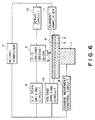
- Figure 6 of the accompanying drawings shows the construction of a memory apparatus according to the prior art in which the electron state is changed to effect recording.
- a movable substrate 2 provided on a coarse movement mechanism 1 there are placed a ground electrode 3 and a recording medium 4 having a switching memory effect, and a probe electrode 6 attached to a three-dimensional (3-D) driving mechanism 5 is provided in opposed relationship with the recording medium 4, and the coarse movement mechanism 1 is first driven by a microcomputer 7 and a coarse movement control circuit 8, whereby rough alignment of the probe electrode 6 and the recording medium 4 is accomplished.
- the probe electrode 6 is scanned on the surface of the recording medium 4 while such a degree of constant voltage that a tunnel current flows is applied between the probe electrode 6 and the recording medium 4.
- the tunnel current obtained at that time is amplified and detected by a current amplifier 11, and the three-dimensional driving mechanism 5 is driven by a servo circuit 12 so that the tunnel current may always assume a predetermined value, whereby the probe electrode 6 is moved in a vertical direction, and the amount of movement in this vertical direction corresponds to recording information. All these controls are effected by the microcomputer 7.
- the probe electrode is brought close to the recording medium 4 up to about 1 nm, and a highly accurate working and manufacturing technique is required of the probe electrode 6 and the recording medium 4.
- the multiprobe system is large in its area in XY direction because multiple probes are parallel-disposed therein, and when generally viewed, there is great amount of variation by a temperature change in this system. Assuming that a temperature change has occurred and the intervals between the adjacent probes have changed, even if a certain probe is tracked to a prescribed position on the recording medium, the other probes will deviate from the prescribed position.
- the memory cartridge according to the present invention in one form thereof has a base having a plurality of probes attached thereto, a substrate on which a recording medium is placed and which is movable relative to said base, and a frame containing said base and said substrate therein, and is characterized in that the coefficients of linear expansion of said base and said substrate are approximated to each other.
- a memory cartridge which has a base having a plurality of probes attached thereto, a substrate on which a recording medium is placed and which is movable relative to said base, and a frame containing said base and said substrate therein and in which the coefficients of linear expansion of said base and said substrate are made approximate to each other, and the system is characterized in that recording or reproduction is effected on said recording medium through said probes.
- Figures 1 to 5 show an embodiment of a memory cartridge according to the present invention and of a memory system using the same, Figure 1 being a cross-sectional view of the system with the memory cartridge inserted in the system body, Figure 2 being an enlarged perspective view illustrating a method of mounting probe electrodes, Figure 3 being an enlarged cross-sectional view of the memory cartridge, Figure 4 being a pictorial perspective view of the memory cartridge, and Figure 5 being a circuit diagram of the system with the memory cartridge inserted in the system body.
- Figure 6 is a circuit diagram of an example of the prior art.
- FIG. 1 is a cross-sectional view of a memory cartridge according to the present invention and a memory system using the same
- the memory cartridge 20 is inserted in a system body 21.
- at least one (in the present embodiment, several hundred) probe electrodes 22 are contained in a frame 24 together with a recording medium 23 and made into a cartridge, which is removably constructed with respect to the system body 21.
- the probe electrodes 22 are formed of tungsten or like material and have a very acute tip end.
- Each probe electrode, as shown in Figure 2 is attached to one end of a bimorph beam 26 which is a cantilever supported on a base 25.
- the cross-sectional construction of the bimorph beam 26 is, for example, an upper electrode (Au)/insulating film (Si3N4)/a piezo layer (ZnO)/insulating film (Si3N4)/an intermediate electrode (Au)/insulating film (Si3N4)/a piezo layer (ZnO)/insulating film (Si3N4)/a lower electrode (Au), and its dimensions may be 750 ⁇ m x 150 ⁇ m and its thickness may be of the order of 7.5 ⁇ m.
- this bimorph beam 26 are polarized in the same direction, voltages of the same polarity, such as positive (negative) for the upper electrode and positive (negative) for the lower electrode, are applied to the upper and lower electrodes relative to the intermediate electrode, whereby the tip end of the bimorph beam 26, i.e., the probe electrode 22, is displaced, and for example, in the case of the above-described cartridge, the amount of displacement of the probe electrode is about 5 ⁇ m for applied voltages of ⁇ 15 V.
- the wiring from each probe electrode 22 and a circuit for conducting the driving voltage of each bimorph beam 26 can be formed on the base 25 and each bimorph beam 26.
- the manufacturing of the probe electrodes 22 and bimorph beams 26 as described above can be accomplished by a method called micromechanics or micromachining [K.E. Petersen, Proc. IEEE 70 , 420 (1982) and T.R. Albrecht et al., 4th International Conference on STM/STS (STM '89) pp. 1-29, S10-2].
- the bases 25 to which the bimorph beams 26 have been attached in this manner are sticked on the inner part of the upper surface of the frame 24 with the tip ends of the probe electrodes 22 facing downward.
- the recording medium 23 is provided on a ground electrode 28 placed on a movable substrate 27, which is supported relative to the frame 24 by packings 29 comprising mechanical seals disposed on the upper and lower surfaces of the end portions of the movable substrate, whereby the recording medium 23 is made movable with the movable substrate 27 in XY direction, i.e., in a horizontal plane, while keeping its distance from the base 25 constant.
- a rectangular window 30 is formed in the lower surface of the frame 24 so that the lower surface of the movable substrate 27 can be seen therethrough, and the XY driving mechanism 31 of the system body 21 is adapted to bear against the movable substrate 27.
- a plurality of electrodes 32 are formed on the lower end portion of the frame 24, and come into contact with an electrode connecting portion 33 provided in the system body 21 when the memory cartridge 20 is inserted into a prescribed position within the system body 21 as indicated by arrow in Figure 1, and they are used for the connection of signals and a power source.
- Electrodes 32 are basically connected to the probe electrodes 22 and the bimorph beams 26 within the frame 24, but as required, at least a portion of a driving circuit which will be described later is contained as a driving circuit 34 in the memory cartridge 20. Materials identical or approximate to each other in coefficient of linear expansion are chosen for the bases 25 and the movable substrate 27.
- the system body 21 is provided with the aforementioned XY driving mechanism 31 movable in XY direction, and a vertically moving mechanism 35 is mechanically connected to the lower portion of the XY driving mechanism 31 so that when the vertically moving mechanism 35 is moved upward, the XY driving mechanism 31 may be inserted into the memory cartridge 20 inserted in the system body 21, through the window 30 and bear against the movable substrate 27.
- a piezo-electric element made into a so-called inch worm construction can be used as the XY driving mechanism.
- a driving circuit as shown in Figure 5 is completed in the system body 21. That is, there are provided an XY scan circuit 40 for scanning and driving the XY driving mechanism 31 in XY direction, a voltage applying circuit 41 for applying a voltage between the probe electrodes 22 and the ground electrode 28, a current amplifier 42 for amplifying a tunnel current flowing between the probe electrodes 22 and the recording medium 23, a servo circuit 43 for adjusting a voltage applied to the bimorph beams 26 so that the current value detected by the use of the current amplifier 42 may become constant, and a microcomputer 44 for effecting the control of the entire system, the analysis of data, etc.
- a coarse movement mechanism, a coarse movement driving circuit, probe electrodes 22, bimorph beams 26 and the accessory circuit thereof are not shown in Figure 5.
- the XY driving mechanism 31 is lowered to a position in which it does not hamper the mounting of the memory cartridge 20 in the direction of arrow in Figure 1, by the vertically moving mechanism 35 and the memory cartridge 20 is mounted into the system body 21, and then the XY driving mechanism 31 is lifted and inserted into the memory cartridge 20 through the window 30 so as to mechanically bear against the movable substrate 27, and during the mounting of the memory cartridge, the electrodes 32 are brought into contact with the electrode connecting portion 33, whereby a driving circuit is completed.
- a voltage is applied to the probe electrodes 22 by the voltage applying circuit 41, and the tunnel current flowing between the probe electrodes 22 and the recording medium 23 is amplified and detected by the current amplifier 42.
- each bimorph beam 26 is controlled by the servo circuit 43, the microcomputer 44, etc., whereby the distance between each probe electrode 22 and the recording medium 23 is controlled and the scanning of the recording medium 23 in XY plane direction is effected by the XY driving mechanism 31 driven by the XY scan circuit 40. Also, where a plurality of probe electrodes 22 are present, the selection thereof can be accomplished by the driving circuit 34 or the microcomputer 44.
- the relative positional deviation between the bases 25 and the movable substrate 27, i.e., between the probe electrodes 22 and the recording medium 23, caused by any temperature change can be reduced and the occurrence of recording and reproduction errors by any temperature change can be decreased.
- Actual recording on the recording medium 23 may be accomplished by one of two methods, i.e., a method of imparting physical deformation to the recording medium 23 and a method of varying the electron state of the recording medium 23.
- a method of imparting physical deformation to the recording medium 23 use is made of a recording medium 23 comprising, for example, a silicon (Si) wafer made integral with the recording medium 23, the ground electrode 28 and the movable substrate 27, and silicon molded articles are also used as the bases 25, and the probe electrodes 22 are urged against the recording medium 23 to physically vary the recording medium 23, thereby accomplishing recording.
- the probe electrodes 22 are two-dimensionally scanned so that the tunnel current may assume a constant value of e.g. 0.1 nA while a DC voltage of e.g. 200 mV is applied to the probe electrodes 22 and the recording medium 23, reproduction can be accomplished because the then feedback driving amount of the bimorph beams 26 corresponds to the recording information on the recording medium 23.
- reproduction experiments in which at room temperature, recording bits are formed on the surface of a silicon wafer in the form of stripes at intervals of about 1 ⁇ m, and then the probe electrode 22 is moved at a constant speed along the direction of the stripes of the bits and the changed position of the detected current is read, have been carried out at a low temperature of 0°C, at room temperature and at a high temperature of 50°C, with a result that in all cases, reproduction bits could be detected at the same intervals. Also, when a germanium (Ge) wafer approximate to silicon in coefficient of linear expansion has been used as the recording medium 23, reproduction bits substantially at the same intervals have been obtained in similar experiments.
- Ge germanium
- the electron state of the surface of the recording medium 23 is varied, for example, six laminated layers of polyimide consisting of pyromellitic acid anhydride formed by the LB technique and 4,4-diaminodiphenyl ether is used as the recording medium 23. If the probe electrodes 22 are brought close to the recording medium 23 and a rectangular wave pulse voltage of 3.5 V and pulse width of 50 ns is applied thereto, the recording medium will cause a change in characteristic (a change in conductivity) and portions of low electrical resistance will be created, whereby recording can be accomplished. Reproduction, as in the other case, can be executed by the detection of a tunnel current, and erasing can be accomplished by a triangular wave pulse voltage of 5 V and pulse width of 1 ⁇ s being applied to the recording medium.
- the memory cartridge described above and the memory system using the same can decrease the occurrence of recording and reproduction errors for any temperature change, and are very useful to put such apparatus into practical use.
- the memory cartridge 20 made into a cartridge by the probe electrodes 22 and the recording medium 23 being contained in the frame 24 as described above is made removable mountable with respect to the system body 21, whereby the alignment of the probe electrodes 22 and the recording medium 23 can be accomplished very accurately and quickly, and such memory cartridge is also high in dust-proof and anti-damage effects.
- portions of high accuracy are made into a unit as the memory cartridge 20, whereby the productivity of the other portions of the system body 21 is improved, and the interchangeability of the portions of high accuracy makes these portions easy to maintain against the damages by accidents or the like.
- the present invention is very effective for a multiprobe system.
- the multiprobe system as shown in the embodiment has multiple probes parallel-disposed and therefore, is large in the area in XY direction, and when generally viewed, it is great in the amount of variation by a temperature change.
- the recording medium side will equally increase and thus, the relative positional relation between each probe and the recording medium will not change. Therefore, in spite of any fluctuation of temperature, all probes can be tracked to the prescribed positions on the medium.
- the recording medium and probes are made into an interchangeable cartridge, but alternatively, provision may be made of a system in which the recording medium is made uninterchangeable and all members are fixed as a unit.
- the technical idea of the present invention is not restricted to the memory system as described above, but can be applied to various kinds of information recording/reproducing apparatuses.
- the recording apparatus mention may be made of an electronic line depicting apparatus for use chiefly for the formation of semiconductor mask patterns which uses probes to depict a minute pattern on a medium.
- the reproducing apparatus mention may be made of a microscope using probe to read the surface condition of a sample, i.e., a so-called STM.
Landscapes
- Micromachines (AREA)
- Length Measuring Devices With Unspecified Measuring Means (AREA)
- Liquid Crystal (AREA)
- Valve Device For Special Equipments (AREA)
- Input Circuits Of Receivers And Coupling Of Receivers And Audio Equipment (AREA)
- Steroid Compounds (AREA)
- Holo Graphy (AREA)
- Semiconductor Memories (AREA)
Applications Claiming Priority (2)
| Application Number | Priority Date | Filing Date | Title |
|---|---|---|---|
| JP280825/90 | 1990-10-19 | ||
| JP2280825A JP2802828B2 (ja) | 1990-10-19 | 1990-10-19 | 情報記録担体及びこれを使用する情報処理装置 |
Publications (3)
| Publication Number | Publication Date |
|---|---|
| EP0481499A2 true EP0481499A2 (de) | 1992-04-22 |
| EP0481499A3 EP0481499A3 (en) | 1993-03-31 |
| EP0481499B1 EP0481499B1 (de) | 1997-09-10 |
Family
ID=17630511
Family Applications (1)
| Application Number | Title | Priority Date | Filing Date |
|---|---|---|---|
| EP91117767A Expired - Lifetime EP0481499B1 (de) | 1990-10-19 | 1991-10-17 | Speicherkassette |
Country Status (6)
| Country | Link |
|---|---|
| US (1) | US5396453A (de) |
| EP (1) | EP0481499B1 (de) |
| JP (1) | JP2802828B2 (de) |
| AT (1) | ATE158099T1 (de) |
| CA (1) | CA2053723C (de) |
| DE (1) | DE69127600T2 (de) |
Cited By (2)
| Publication number | Priority date | Publication date | Assignee | Title |
|---|---|---|---|---|
| EP0603770A2 (de) * | 1992-12-21 | 1994-06-29 | Canon Kabushiki Kaisha | Informationsaufzeichnungs-/wiedergabegerät zur Informationsaufzeichnung und /-wiedergabe mittels einer Sondenelektrode |
| EP0838302A1 (de) * | 1996-09-10 | 1998-04-29 | Hewlett-Packard Company | Positioniervorrichtung |
Families Citing this family (23)
| Publication number | Priority date | Publication date | Assignee | Title |
|---|---|---|---|---|
| DE69031053T2 (de) * | 1989-04-25 | 1998-01-29 | Canon Kk | Informationsaufzeichnungs-/Wiedergabegerät und Informationsaufzeichnungsträger |
| DE69230198T2 (de) * | 1991-07-17 | 2000-07-06 | Canon Kk | Informationsaufzeichnungs-/Wiedergabegrät zur Informationsaufzeichnung und/oder -wiedergabe auf/von einem Informationsaufzeichnungsträger durch Benutzung einer Sonde. |
| JP3135779B2 (ja) * | 1994-03-18 | 2001-02-19 | キヤノン株式会社 | 情報処理装置 |
| US5874668A (en) | 1995-10-24 | 1999-02-23 | Arch Development Corporation | Atomic force microscope for biological specimens |
| US7260051B1 (en) | 1998-12-18 | 2007-08-21 | Nanochip, Inc. | Molecular memory medium and molecular memory integrated circuit |
| US20020138301A1 (en) * | 2001-03-22 | 2002-09-26 | Thanos Karras | Integration of a portal into an application service provider data archive and/or web based viewer |
| US7233517B2 (en) * | 2002-10-15 | 2007-06-19 | Nanochip, Inc. | Atomic probes and media for high density data storage |
| FR2869027B1 (fr) * | 2004-04-15 | 2006-07-14 | Commissariat Energie Atomique | Systeme d'enregistrement comportant une couche memoire et un reseau de micro-pointes |
| US20050243660A1 (en) * | 2004-04-16 | 2005-11-03 | Rust Thomas F | Methods for erasing bit cells in a high density data storage device |
| US20050243592A1 (en) * | 2004-04-16 | 2005-11-03 | Rust Thomas F | High density data storage device having eraseable bit cells |
| US7463573B2 (en) * | 2005-06-24 | 2008-12-09 | Nanochip, Inc. | Patterned media for a high density data storage device |
| US20070041237A1 (en) * | 2005-07-08 | 2007-02-22 | Nanochip, Inc. | Media for writing highly resolved domains |
| US20060291271A1 (en) * | 2005-06-24 | 2006-12-28 | Nanochip, Inc. | High density data storage devices having servo indicia formed in a patterned media |
| US7367119B2 (en) * | 2005-06-24 | 2008-05-06 | Nanochip, Inc. | Method for forming a reinforced tip for a probe storage device |
| US20070008866A1 (en) * | 2005-07-08 | 2007-01-11 | Nanochip, Inc. | Methods for writing and reading in a polarity-dependent memory switch media |
| US20070008867A1 (en) * | 2005-07-08 | 2007-01-11 | Nanochip, Inc. | High density data storage devices with a lubricant layer comprised of a field of polymer chains |
| US7309630B2 (en) | 2005-07-08 | 2007-12-18 | Nanochip, Inc. | Method for forming patterned media for a high density data storage device |
| JP4817465B2 (ja) * | 2006-10-05 | 2011-11-16 | パイオニア株式会社 | 記録再生装置 |
| US7903532B2 (en) * | 2006-10-11 | 2011-03-08 | Seagate Technology Llc | Elevated electrodes for probe position sensing |
| US20080175033A1 (en) * | 2007-01-19 | 2008-07-24 | Nanochip, Inc. | Method and system for improving domain stability in a ferroelectric media |
| US20080233672A1 (en) * | 2007-03-20 | 2008-09-25 | Nanochip, Inc. | Method of integrating mems structures and cmos structures using oxide fusion bonding |
| US20090129246A1 (en) * | 2007-11-21 | 2009-05-21 | Nanochip, Inc. | Environmental management of a probe storage device |
| US20100039729A1 (en) * | 2008-08-14 | 2010-02-18 | Nanochip, Inc. | Package with integrated magnets for electromagnetically-actuated probe-storage device |
Citations (8)
| Publication number | Priority date | Publication date | Assignee | Title |
|---|---|---|---|---|
| DE3637684A1 (de) * | 1985-11-05 | 1987-05-07 | Sharp Kk | Elektronisches geraet mit einsteckbarer speicherkarte |
| JPS6325878A (ja) * | 1986-07-18 | 1988-02-03 | Asahi Glass Co Ltd | メモリ−カ−トリツジ |
| EP0272935A2 (de) * | 1986-12-24 | 1988-06-29 | Canon Kabushiki Kaisha | Aufnahmegerät und Wiedergabegerät |
| EP0307210A2 (de) * | 1987-09-10 | 1989-03-15 | Seiko Instruments Inc. | Speicher-Schreibgerät |
| WO1989007259A2 (en) * | 1988-01-27 | 1989-08-10 | The Board Of Trustees Of The Leland Stanford Junio | Integrated scanning tunneling microscope |
| FR2637409A1 (fr) * | 1988-10-05 | 1990-04-06 | Olympus Optical Co | Memoire pour ordinateur |
| EP0368579A2 (de) * | 1988-11-09 | 1990-05-16 | Canon Kabushiki Kaisha | Sondeneinheit, Betriebsverfahren und Rastervorrichtung zur Feststellung eines Tunnelstromes mit dieser Sonde |
| WO1990015986A1 (en) * | 1989-06-20 | 1990-12-27 | The Board Of Trustees Of The Leland Stanford Junior University | Microfabricated microscope assembly |
Family Cites Families (6)
| Publication number | Priority date | Publication date | Assignee | Title |
|---|---|---|---|---|
| JP2757887B2 (ja) * | 1986-02-17 | 1998-05-25 | 株式会社島津製作所 | 情報を記録し,および読出す方法 |
| JPS63138579A (ja) * | 1986-11-29 | 1988-06-10 | Sony Corp | ヘツドア−ム装置 |
| JP2556492B2 (ja) * | 1986-12-24 | 1996-11-20 | キヤノン株式会社 | 再生装置及び再生法 |
| JP2556491B2 (ja) * | 1986-12-24 | 1996-11-20 | キヤノン株式会社 | 記録装置及び記録法 |
| JPH0246573A (ja) * | 1988-08-09 | 1990-02-15 | Mitsubishi Electric Corp | フレキシブルデイスク装置のヘツド位置決め機構 |
| US5075548A (en) * | 1989-07-17 | 1991-12-24 | Olympus Optical Co., Ltd. | Tunnel current probe moving mechanism having parallel cantilevers |
-
1990
- 1990-10-19 JP JP2280825A patent/JP2802828B2/ja not_active Expired - Fee Related
-
1991
- 1991-10-17 EP EP91117767A patent/EP0481499B1/de not_active Expired - Lifetime
- 1991-10-17 DE DE69127600T patent/DE69127600T2/de not_active Expired - Fee Related
- 1991-10-17 AT AT91117767T patent/ATE158099T1/de not_active IP Right Cessation
- 1991-10-18 CA CA002053723A patent/CA2053723C/en not_active Expired - Fee Related
-
1994
- 1994-07-06 US US08/272,373 patent/US5396453A/en not_active Expired - Fee Related
Patent Citations (9)
| Publication number | Priority date | Publication date | Assignee | Title |
|---|---|---|---|---|
| DE3637684A1 (de) * | 1985-11-05 | 1987-05-07 | Sharp Kk | Elektronisches geraet mit einsteckbarer speicherkarte |
| JPS6325878A (ja) * | 1986-07-18 | 1988-02-03 | Asahi Glass Co Ltd | メモリ−カ−トリツジ |
| EP0272935A2 (de) * | 1986-12-24 | 1988-06-29 | Canon Kabushiki Kaisha | Aufnahmegerät und Wiedergabegerät |
| EP0307210A2 (de) * | 1987-09-10 | 1989-03-15 | Seiko Instruments Inc. | Speicher-Schreibgerät |
| WO1989007259A2 (en) * | 1988-01-27 | 1989-08-10 | The Board Of Trustees Of The Leland Stanford Junio | Integrated scanning tunneling microscope |
| WO1989007256A1 (en) * | 1988-01-27 | 1989-08-10 | The Board Of Trustees Of The Leland Stanford Junio | An integrated mass storage device |
| FR2637409A1 (fr) * | 1988-10-05 | 1990-04-06 | Olympus Optical Co | Memoire pour ordinateur |
| EP0368579A2 (de) * | 1988-11-09 | 1990-05-16 | Canon Kabushiki Kaisha | Sondeneinheit, Betriebsverfahren und Rastervorrichtung zur Feststellung eines Tunnelstromes mit dieser Sonde |
| WO1990015986A1 (en) * | 1989-06-20 | 1990-12-27 | The Board Of Trustees Of The Leland Stanford Junior University | Microfabricated microscope assembly |
Cited By (4)
| Publication number | Priority date | Publication date | Assignee | Title |
|---|---|---|---|---|
| EP0603770A2 (de) * | 1992-12-21 | 1994-06-29 | Canon Kabushiki Kaisha | Informationsaufzeichnungs-/wiedergabegerät zur Informationsaufzeichnung und /-wiedergabe mittels einer Sondenelektrode |
| EP0603770A3 (de) * | 1992-12-21 | 1995-12-13 | Canon Kk | Informationsaufzeichnungs-/wiedergabegerät zur Informationsaufzeichnung und /-wiedergabe mittels einer Sondenelektrode. |
| EP0838302A1 (de) * | 1996-09-10 | 1998-04-29 | Hewlett-Packard Company | Positioniervorrichtung |
| US6501210B1 (en) | 1996-09-10 | 2002-12-31 | Hewlett-Packard Company | Positioning mechanism having elongate bending elements oriented perpendicular to the direction of movement |
Also Published As
| Publication number | Publication date |
|---|---|
| ATE158099T1 (de) | 1997-09-15 |
| US5396453A (en) | 1995-03-07 |
| DE69127600T2 (de) | 1998-03-19 |
| JPH04157640A (ja) | 1992-05-29 |
| CA2053723A1 (en) | 1992-04-20 |
| EP0481499B1 (de) | 1997-09-10 |
| EP0481499A3 (en) | 1993-03-31 |
| CA2053723C (en) | 1997-06-24 |
| DE69127600D1 (de) | 1997-10-16 |
| JP2802828B2 (ja) | 1998-09-24 |
Similar Documents
| Publication | Publication Date | Title |
|---|---|---|
| CA2053723C (en) | Recording/reproducing apparatus such as a memory apparatus | |
| US5412641A (en) | Information recording/reproducing apparatus for recording/reproducing information with probes | |
| EP0511763B1 (de) | Sonde mit freitragendem Arm, sowie Rastertunnelstrommikroskop und Informationsverarbeitungsgerät welches dieselbe verwendet | |
| CA2055852C (en) | Slope detection method, and information detection/writing apparatus using the method | |
| US5461605A (en) | Information recording/reproducing method, recording carrier and apparatus for recording and/or reproducing information on information recording carrier by use of probe electrode | |
| EP0452852B1 (de) | Gerät zur Informationsaufzeichnung und/oder -wiedergabe | |
| CA2069708C (en) | Probe-driving mechanism, production thereof, and apparatus and piezoelectric actuator employing the same | |
| EP0325056A2 (de) | Datenspeichervorrichtung | |
| JP3135779B2 (ja) | 情報処理装置 | |
| JPH05284765A (ja) | カンチレバー型変位素子、及びこれを用いたカンチレバー型プローブ、及びこのカンチレバー型プローブを用いた走査型トンネル顕微鏡並びに情報処理装置 | |
| US5251200A (en) | Tracking method for memory apparatus | |
| EP0481498B1 (de) | Informationsaufzeichnungseinheit und Gerät und Verfahren zur Informationsaufzeichnung/-wiedergabe | |
| US5371728A (en) | Information recording/reproducing apparatus using probe | |
| JP3234722B2 (ja) | 円弧状反りレバー型アクチュエータ、該アクチュエータの駆動方法及び情報入出力用プローブを用いた情報処理装置 | |
| JP2934037B2 (ja) | 情報記録及び/又は再生装置 | |
| JP2934057B2 (ja) | プローブユニット及びこれを使用する情報記録及び/又は再生装置 | |
| JPH07110969A (ja) | 面合わせ方法,位置制御機構および該機構を有する情報処理装置 | |
| JPH11102545A (ja) | 情報処理装置 | |
| JP2946132B2 (ja) | 情報処理装置及び情報処理用カセット | |
| JP2995126B2 (ja) | 情報処理装置 | |
| JPH04330653A (ja) | 情報再生装置及び情報記録再生装置 | |
| JPH0714224A (ja) | 記録媒体及び情報処理装置 | |
| JPH04223203A (ja) | カンチレバー型プローブ、これを用いた情報処理装置及び情報処理方法 | |
| JPH04157639A (ja) | 情報記録担体及びこれを使用する情報処理装置 | |
| JPH04157642A (ja) | 情報記録担体及びこれを使用する情報処理装置 |
Legal Events
| Date | Code | Title | Description |
|---|---|---|---|
| PUAI | Public reference made under article 153(3) epc to a published international application that has entered the european phase |
Free format text: ORIGINAL CODE: 0009012 |
|
| AK | Designated contracting states |
Kind code of ref document: A2 Designated state(s): AT BE CH DE DK ES FR GB GR IT LI LU NL SE |
|
| PUAL | Search report despatched |
Free format text: ORIGINAL CODE: 0009013 |
|
| AK | Designated contracting states |
Kind code of ref document: A3 Designated state(s): AT BE CH DE DK ES FR GB GR IT LI LU NL SE |
|
| 17P | Request for examination filed |
Effective date: 19930817 |
|
| 17Q | First examination report despatched |
Effective date: 19950329 |
|
| GRAG | Despatch of communication of intention to grant |
Free format text: ORIGINAL CODE: EPIDOS AGRA |
|
| GRAH | Despatch of communication of intention to grant a patent |
Free format text: ORIGINAL CODE: EPIDOS IGRA |
|
| GRAH | Despatch of communication of intention to grant a patent |
Free format text: ORIGINAL CODE: EPIDOS IGRA |
|
| GRAA | (expected) grant |
Free format text: ORIGINAL CODE: 0009210 |
|
| AK | Designated contracting states |
Kind code of ref document: B1 Designated state(s): AT BE CH DE DK ES FR GB GR IT LI LU NL SE |
|
| PG25 | Lapsed in a contracting state [announced via postgrant information from national office to epo] |
Ref country code: LI Free format text: LAPSE BECAUSE OF FAILURE TO SUBMIT A TRANSLATION OF THE DESCRIPTION OR TO PAY THE FEE WITHIN THE PRESCRIBED TIME-LIMIT Effective date: 19970910 Ref country code: AT Effective date: 19970910 Ref country code: BE Effective date: 19970910 Ref country code: CH Free format text: LAPSE BECAUSE OF FAILURE TO SUBMIT A TRANSLATION OF THE DESCRIPTION OR TO PAY THE FEE WITHIN THE PRESCRIBED TIME-LIMIT Effective date: 19970910 Ref country code: GR Free format text: LAPSE BECAUSE OF FAILURE TO SUBMIT A TRANSLATION OF THE DESCRIPTION OR TO PAY THE FEE WITHIN THE PRESCRIBED TIME-LIMIT Effective date: 19970910 Ref country code: NL Free format text: LAPSE BECAUSE OF FAILURE TO SUBMIT A TRANSLATION OF THE DESCRIPTION OR TO PAY THE FEE WITHIN THE PRESCRIBED TIME-LIMIT Effective date: 19970910 Ref country code: ES Free format text: THE PATENT HAS BEEN ANNULLED BY A DECISION OF A NATIONAL AUTHORITY Effective date: 19970910 Ref country code: DK Free format text: LAPSE BECAUSE OF NON-PAYMENT OF DUE FEES Effective date: 19970910 |
|
| REF | Corresponds to: |
Ref document number: 158099 Country of ref document: AT Date of ref document: 19970915 Kind code of ref document: T |
|
| REG | Reference to a national code |
Ref country code: CH Ref legal event code: EP |
|
| REF | Corresponds to: |
Ref document number: 69127600 Country of ref document: DE Date of ref document: 19971016 |
|
| PG25 | Lapsed in a contracting state [announced via postgrant information from national office to epo] |
Ref country code: LU Free format text: LAPSE BECAUSE OF NON-PAYMENT OF DUE FEES Effective date: 19971017 |
|
| ET | Fr: translation filed | ||
| ITF | It: translation for a ep patent filed |
Owner name: SOCIETA' ITALIANA BREVETTI S.P.A. |
|
| PG25 | Lapsed in a contracting state [announced via postgrant information from national office to epo] |
Ref country code: SE Effective date: 19971210 |
|
| NLV1 | Nl: lapsed or annulled due to failure to fulfill the requirements of art. 29p and 29m of the patents act | ||
| REG | Reference to a national code |
Ref country code: CH Ref legal event code: PL |
|
| PLBE | No opposition filed within time limit |
Free format text: ORIGINAL CODE: 0009261 |
|
| STAA | Information on the status of an ep patent application or granted ep patent |
Free format text: STATUS: NO OPPOSITION FILED WITHIN TIME LIMIT |
|
| 26N | No opposition filed | ||
| REG | Reference to a national code |
Ref country code: GB Ref legal event code: IF02 |
|
| PGFP | Annual fee paid to national office [announced via postgrant information from national office to epo] |
Ref country code: FR Payment date: 20051010 Year of fee payment: 15 |
|
| PGFP | Annual fee paid to national office [announced via postgrant information from national office to epo] |
Ref country code: GB Payment date: 20051012 Year of fee payment: 15 |
|
| PGFP | Annual fee paid to national office [announced via postgrant information from national office to epo] |
Ref country code: DE Payment date: 20051014 Year of fee payment: 15 |
|
| PGFP | Annual fee paid to national office [announced via postgrant information from national office to epo] |
Ref country code: IT Payment date: 20061031 Year of fee payment: 16 |
|
| PG25 | Lapsed in a contracting state [announced via postgrant information from national office to epo] |
Ref country code: DE Free format text: LAPSE BECAUSE OF NON-PAYMENT OF DUE FEES Effective date: 20070501 |
|
| GBPC | Gb: european patent ceased through non-payment of renewal fee |
Effective date: 20061017 |
|
| REG | Reference to a national code |
Ref country code: FR Ref legal event code: ST Effective date: 20070629 |
|
| PG25 | Lapsed in a contracting state [announced via postgrant information from national office to epo] |
Ref country code: GB Free format text: LAPSE BECAUSE OF NON-PAYMENT OF DUE FEES Effective date: 20061017 |
|
| PG25 | Lapsed in a contracting state [announced via postgrant information from national office to epo] |
Ref country code: FR Free format text: LAPSE BECAUSE OF NON-PAYMENT OF DUE FEES Effective date: 20061031 |
|
| PG25 | Lapsed in a contracting state [announced via postgrant information from national office to epo] |
Ref country code: IT Free format text: LAPSE BECAUSE OF NON-PAYMENT OF DUE FEES Effective date: 20071017 |