EP0476584A1 - Dynamischer Speicher mit wahlfreiem Zugriff mit erhöhtem Kontakt - Google Patents
Dynamischer Speicher mit wahlfreiem Zugriff mit erhöhtem Kontakt Download PDFInfo
- Publication number
- EP0476584A1 EP0476584A1 EP91115749A EP91115749A EP0476584A1 EP 0476584 A1 EP0476584 A1 EP 0476584A1 EP 91115749 A EP91115749 A EP 91115749A EP 91115749 A EP91115749 A EP 91115749A EP 0476584 A1 EP0476584 A1 EP 0476584A1
- Authority
- EP
- European Patent Office
- Prior art keywords
- memory cell
- insulation layer
- major surface
- layer
- region
- Prior art date
- Legal status (The legal status is an assumption and is not a legal conclusion. Google has not performed a legal analysis and makes no representation as to the accuracy of the status listed.)
- Granted
Links
Images


Classifications
-
- H—ELECTRICITY
- H01—ELECTRIC ELEMENTS
- H01L—SEMICONDUCTOR DEVICES NOT COVERED BY CLASS H10
- H01L21/00—Processes or apparatus adapted for the manufacture or treatment of semiconductor or solid state devices or of parts thereof
- H01L21/70—Manufacture or treatment of devices consisting of a plurality of solid state components formed in or on a common substrate or of parts thereof; Manufacture of integrated circuit devices or of parts thereof
- H01L21/71—Manufacture of specific parts of devices defined in group H01L21/70
- H01L21/768—Applying interconnections to be used for carrying current between separate components within a device comprising conductors and dielectrics
- H01L21/76801—Applying interconnections to be used for carrying current between separate components within a device comprising conductors and dielectrics characterised by the formation and the after-treatment of the dielectrics, e.g. smoothing
- H01L21/76802—Applying interconnections to be used for carrying current between separate components within a device comprising conductors and dielectrics characterised by the formation and the after-treatment of the dielectrics, e.g. smoothing by forming openings in dielectrics
-
- H—ELECTRICITY
- H01—ELECTRIC ELEMENTS
- H01L—SEMICONDUCTOR DEVICES NOT COVERED BY CLASS H10
- H01L23/00—Details of semiconductor or other solid state devices
- H01L23/52—Arrangements for conducting electric current within the device in operation from one component to another, i.e. interconnections, e.g. wires, lead frames
- H01L23/522—Arrangements for conducting electric current within the device in operation from one component to another, i.e. interconnections, e.g. wires, lead frames including external interconnections consisting of a multilayer structure of conductive and insulating layers inseparably formed on the semiconductor body
- H01L23/5222—Capacitive arrangements or effects of, or between wiring layers
-
- H—ELECTRICITY
- H10—SEMICONDUCTOR DEVICES; ELECTRIC SOLID-STATE DEVICES NOT OTHERWISE PROVIDED FOR
- H10B—ELECTRONIC MEMORY DEVICES
- H10B12/00—Dynamic random access memory [DRAM] devices
- H10B12/30—DRAM devices comprising one-transistor - one-capacitor [1T-1C] memory cells
- H10B12/31—DRAM devices comprising one-transistor - one-capacitor [1T-1C] memory cells having a storage electrode stacked over the transistor
-
- H—ELECTRICITY
- H01—ELECTRIC ELEMENTS
- H01L—SEMICONDUCTOR DEVICES NOT COVERED BY CLASS H10
- H01L2924/00—Indexing scheme for arrangements or methods for connecting or disconnecting semiconductor or solid-state bodies as covered by H01L24/00
- H01L2924/0001—Technical content checked by a classifier
- H01L2924/0002—Not covered by any one of groups H01L24/00, H01L24/00 and H01L2224/00
Definitions
- the present invention generally relates to semiconductor memory devices and more particularly to a random access memory providing a reliable contact for interconnections.
- SOG spin-on-glass
- an organic solution of silicon is applied on the surface of the insulation layer and cured by evaporating the solvents.
- This technique although effective in planarizing the surface of an insulator layer, tends to cause a problem of defective interconnections when the interconnection pattern such as aluminum pattern is provided in contact directly with the SOG layer. It is believed that organic vapors as well as the water vapor that are released from the SOG causes such a degradation of the contact. It should be noted that SOG generally releases volatile components even after the curing. Because of this reason, an insulation layer such as silicon oxide or PSG is provided further on the SOG layer by the CVD process to support the interconnection pattern such that the interconnection pattern is separated from the SOG layer.
- the insulator layer underlying the SOG layer contacts directly with the insulator layer provided on the SOG layer in correspondence to the region where the contact hole is to be formed, and the SOG layer is excluded from the contact hole.
- the SOG layer is not exposed at the side wall of the contact hole and a reliable electric contact is achieved.
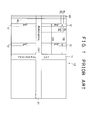
- FIG.1 shows the overall construction of a conventional DRAM chip 10.
- the surface of the DRAM chip 10 is divided into a number of generally rectangular regions by the peripheral circuits 11 that are arranged along a zone extending laterally and vertically throughout the chip 10.
- the zones cross with each other generally at a central part of the chip 10.
- a number of columnar zones 12 are provided to extend vertically in the drawing with a regular interval for accommodating the sense amplifiers S/A.
- memory cells Adjacent to the zones 12, memory cells (not shown specifically in FIG.1) are provided in the row and column formation to form a memory cell region.
- a word line WL is provided to extend vertically as shown in FIG.1.
- complementary bit lines BL and BL are provided to extend laterally as shown in FIG.1.
- each sense amplifier in the zone 12 is connected to the sense amplifiers on the same row of other columns via a data bus line DB that extends laterally through the chip 10.
- the data bus line DB thereby extends in the row direction and connects the sense amplifiers S/A aligned on the same row to the peripheral circuit 11. It should be noted that there are a number of data bus lines DB extending laterally across the surface of the chip.
- FIG.2 shows a typical construction of a part of the memory cell, wherein the memory cell includes a plurality of transistor T11, T13, T22, ... arranged in rows and columns.
- the transistors T11 and T13 are connected commonly to a bit line BL extending in the row direction, while the transistor T22 is connected to another, complementary bit line BL.
- each transistor is connected to a corresponding word line WL1, WL2, WL3, ....
- the transistor T11 has a source connected to the bit line BL.
- the transistor T13 has a source connected to the same bit line BL.
- the transistor T22 on the other hand has a source connected to the complementary bit line BL.
- the transistors T11, T22, T13 have respective drains connected to the memory cell capacitor.
- the word lines WL1 - WL3 are connected to the respective gates of the transistors T11, T22, T13.
- FIG.3 shows the circuit diagram of the sense amplifier S/A.
- the sense amplifier includes P-channel MOS transistors Q1 and Q3 as well as N-channel MOS transistors Q2 and Q4, wherein the transistors Q1 and Q2 are connected in series to form a first path while the transistors Q3 and Q4 are connected in series to form a second path.
- the sense amplifier S/A is formed by connecting the first path and the second path in parallel between a supply voltage Vcc and another supply voltage Vss.
- bit line BL is connected commonly to the respective drains of the transistors Q1 and Q2 and further to respective gates of the transistors Q3 and Q4.
- the bit line BL is connected to the respective drains of the transistors Q3 and Q4, and further to the respective gates of the transistors Q1 and Q2.
- the bit lines BL and BL has to cross with each other in the region of the sense amplifier S/A.
- FIG.4 shows such a crossing of the bit lines BL and BL in the sense amplifier S/A.
- the bit line BL is connected once to a conductor strip located underneath the bit line by a contact hole. As will be described later, this conductor strip is formed at the time of formation of the word line WL as a part of the conductor layer forming the word line WL.
- the complementary bit line BL extends over the conductor pattern, separated of course by an insulation layer not illustrated, and the crossing of the bit line BL and BL is achieved as illustrated.
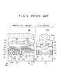
- FIG.5 shows a cross sectional view of the conventional DRAM including the memory cell region and the sense amplifier region, wherein the sense amplifier region shows the cross section taken along the line 5-5' of FIG.4.
- the DRAM is constructed on a device region that is defined on the upper major surface of a silicon substrate 21 by a field oxide region 22.
- a gate electrode 23 of polysilicon is provided on the device region with a gate oxide film 23a intervening between the gate electrode 23 and the upper major surface of the substrate 21, and a silicon oxide layer 24 is provided for example by the CVD process to bury the gate electrode 23 underneath.
- the gate electrode 23 is formed as a part of the word line WL that is extending through the DRAM chip 10. As shown in FIG.1, there are a number of word lines WL extending parallel, and the cross section of FIG.5 shows another word line WL that extends over the field oxide region 22.
- the silicon oxide layers 24 and 25 are formed with a contact hole that exposes the upper major surface of the substrate 21 in correspondence to a diffusion region 21 a acting as a source of the memory cell transistor, and a polysilicon electrode 26 is provided to extend from the upper major surface of the diffusion region 21 a along the upper major surface of the silicon oxide layer 25 to form the bit line BL.
- the electrode 26 extends obliquely to the plane of the drawing and shows an appearance in the illustration of FIG.5 that the electrode 26 is interrupted at an intermediate position, covering the silicon oxide layer 25 only partially.
- the polysilicon electrode 26 is covered by a silicon oxide film 27 that buries the electrode 26 as well as the silicon oxide layer 25 underneath.
- the field oxide region 22 it will be seen thereby that a consecutive deposition of the silicon oxide layers 24, 25 and 27 is made such that these layers bury the polysilicon word line WL on the field oxide region 22.
- a through hole 24a that exposes the upper major surface of the diffusion region 21 acting as a drain of the memory cell transistor, and there is formed a polysilicon electrode 28 that extends upward along the side wall of the through hole 24a and spreads laterally at a level above the silicon oxide layer 27 to form a stacked capacitor C characterized by a large surface area.
- the electrode 28 is covered by a thin dielectric film 28a such as silicon oxide (not shown), and a ground electrode 29 of polysilicon covers the fin part of the electrode 28.
- a silicon nitride film 30 for protecting the silicon oxide layer 27 from etching at the time of forming the fin structure.
- an insulation layer 31 of PSG (phosphosilicate glass) or BPSG (boro- phosphosilicate glass) is provided to extend throughout the chip 10.
- the insulation layer 31 extends also over the sense amplifier region 12.
- the word bus line WB is used for distributing the word line voltage efficiently over the memory cells on the chip and establishes a contact with the polysilicon word line at a suitable contact hole.
- the word bus line WB is buried under an insulation layer 34 such as PSG or BPSG that in turn is provided on an SOG layer 35 that fills the depressed regions formed between the word bus lines WB. Thereby, the SOG layer 35 improves the planarization of the insulation layer 34.
- the data bus line DB shown in FIG.1 is provided for interconnection with the sense amplifiers.
- the insulation layer 31, the SOG layer 35 and the insulation layer 34 are provided in correspondence to the memory cell region.
- an aluminum pattern 33 is provided on the insulation layer 31 in correspondence to the word bus lines WB, and the data bus line DB establishes a contact with the aluminum pattern 33 via a contact hole 34a that penetrates through the layer 34 as well as the SOG layer 35.
- the aluminum pattern 33 in turn is connected to the sense amplifier at a site not shown in FIG.5.
- this contact hole 34a is generally formed between a pair of bit lines extending parallel with each other.
- each of the parallel bit lines includes a first conductor strip 23' that is formed simultaneously with the word line WL by patterning a common polysilicon layer, and a second conductor strip 26' that is formed simultaneously with the bit lines BL and BL by patterning a common polysilicon layer.
- the aluminum pattern 33 is provided on the lowest part of the insulation layer 31 located between a pair of ridges corresponding to the polysilicon patterns 23' and 26', there occurs an accumulation of the SOG on the upper major surface of the pattern 33, and this accumulated SOG layer is exposed at the side wall of the contact hole 34a.
- bit lines BL, BL and the word lines WL are patterned within the accuracy of ⁇ 0.5 /1.m as for the positional deviation, while the word line bus WB or data bus DB is usually patterned with the accuracy of ⁇ 1 /1.m.
- Another and more specific object of the present invention is to provide a dynamic random access memory having an improved reliability.
- Another object of the present invention is to provide a method of fabricating a dynamic random access memory with an improved yield and reduced cost.
- Another object of the present invention is to provide a dynamic random access memory comprising a memory cell region and a sense amplifier region formed on a substrate, said memory cell region including a MOS transistor having a gate provided on an upper major surface of said substrate, said gate extending along the upper major surface of the substrate and forming a word line, a first diffusion region provided in said substrate adjacent to said gate as a source region and a second diffusion region provided in said substrate adjacent to said gate at a side opposite to the first diffusion region as a drain region, said memory cell region further including a bit line connected to the first diffusion region and extending along the upper major surface of the substrate at a level above the word line, a stacked capacitor structure connected to the second diffusion region and extending in an upward direction, a first insulation layer provided on said MOS transistor for burying the stacked capacitor structure underneath, said first insulation layer further burying the word lines and bit lines underneath, a first interconnection pattern provided on an upper major surface of the first insulation layer, an SOG layer provided on the first insulation layer for filling depressions formed
- the present invention one can exclude the SOG layer at the part where the contact hole is to be formed.
- the fourth insulation layer is contacted directly on the upper major surface of the conductor pattern 33 as a result of the lifting of the conductor pattern that in turn is caused by the projection member, and the SOG layer 35 is eliminated from the contact hole 34a.
- FIG.6 shows an embodiment of DRAM according to the present invention.
- the parts that correspond to those parts already described with reference to FIG.5 are designated by the same reference numerals and the description will not be repeated.
- a projection structure 38 formed of a silicon nitride pattern 36 and a polysilicon pattern 37 on the depressed upper major surface of the silicon oxide layer 27, wherein the silicon nitride pattern 36 is provided directly on the depressed upper major surface of the silicon oxide layer 27 and the polysilicon pattern 37 is provided on the silicon nitride pattern 36.
- the silicon nitride pattern 36 is formed from the same silicon nitride film that forms the silicon nitride film 30 of the stacked capacitor C. As is commonly practiced, this silicon nitride film 30 is used for the etching stopper at the time of forming a space under the polysilicon fin of the electrode 28 for the electrode 29 that fills the space. In the conventional device, this silicon nitride film has been removed after the formation of the electrode 29 except for the film 30 that is located under the electrode 29.
- the polysilicon pattern 37 on the silicon nitride pattern 36 is formed from the same polysilicon film that forms the electrode 29 of the stacked capacitor C. In the conventional device, this polysilicon layer 37 has been removed by etching after the formation of the electrode 28.
- the patterns 36 and 37 are formed with the accuracy or design rule used for forming the word lines WL and the bit lines BL. Thereby, the patterns 36 and 37 typically have a width W of about 1.5 /1.m. With such a strict design rule applied, it is easy to form the patterns 36 and 37 exactly in correspondence to the depression formed on the upper major surface of the silicon oxide layer 27.
- the insulation layer 31 that buries the projection structure 38 underneath shows a substantially flat upper major surface in spite of the fact that there is a depression in the silicon oxide layer 27.
- the position of the aluminum conductor pattern 33 provided on the insulation layer 31 is moved upward and the top surface of the pattern 33 is exposed above the insulation layer 35.
- the pattern 33 is formed with a less strict design rule and the pattern 33 may not be formed at the exact position as shown in FIG.6.
- such a lateral deviation in the pattern 33 does not cause problem at all, as the surface of the insulation layer 31 is substantially flat and the upper surface of the conductor pattern 33 is exposed above the SOG layer irrespective of where the pattern 33 is provided.
- the insulation layer 34 makes a direct contact with the exposed upper major surface of the conductor pattern 33.
- the SOG layer 35 is excluded from the contact hole 34a that is provided on the insulator layer 34 to expose the upper major surface of the conductor pattern 33, and a reliable electric contact can be established between the data bus DB and the conductor pattern 33.
- a thin insulation film 35a of BPSG may be formed to cover the aluminum patterns WB or 33 for preventing the formation of hilloks.
- This BPSG layer 35a has an extremely limited thickness and does not influence the effectiveness of the structure of FIG.6.
- the contact hole 34a is formed to penetrate through this thin BPSG layer 35a.
- a field oxide region 22 is formed on the upper major surface of the silicon substrate 21 by the LOCOS process to define a device region. It should be noted that the device region is formed in the memory cell region defined in FIG.1.
- the exposed upper major surface of the silicon substrate 21 is covered with a thin silicon oxide film, and the word lines WL of polysilicon are formed on the substrate to extend generally parallel with each other over the device region by a predetermined pitch, by depositing a polysilicon layer (not shown) and patterning the same subsequently.
- the word line WL forms the gate electrode 23 in the device region and establishes a contact to the upper major surface of the silicon substrate 21 via the thin oxide film formed previously. This oxide film acts as the gate oxide film.
- an ion implantation process is conducted to form the source region 21 a and the drain region 21 b in the substrate at both sides of the gate electrode 23.
- the patterning of the polysilicon layer is achieved simultaneously in the sense amplifier region shown at the right of FIG.7-(A) as well as in the memory cell region shown at the left.
- the polysilicon patterns 23' are formed on the upper major surface of the substrate 21 simultaneously to the word lines WL from the same polysilicon layer that have formed that word line WL and the gate electrode 23.
- the patterns 23' are separated from the upper major surface of the substrate 21 by the thin silicon oxide film that was formed to cover the entire exposed surface of the substrate 21 after the LOCOS process has been accomplished, as already described.
- the silicon oxide layer 24 is deposited by the CVD process to bury the word lines WL including the gate electrode 23 of the memory cell region and the pattern 23' of the sense amplifier region. Further, another silicon oxide layer 25 is deposited on the silicon oxide layer 24, and another polysilicon layer (not shown) is deposited further on the layer 25 after forming a contact hole exposing the source region 21 a of the MOS transistor. By patterning the second polysilicon layer, the bit lines 26 are formed in contact with the source region 21a. Simultaneously, the polysilicon patterns 26' are formed on the insulator layer 25 from the same second polysilicon layer. In the illustrated example, the silicon oxide layer 24 is removed from the region above the polysilicon pattern 23' of the sense amplifier region. Thereby, the silicon oxide layer 25 directly covers the pattern 23' and the upper major surface of the substrate 21.
- the silicon oxide layer 27 is deposited by the CVD process to cover the entire structure. Further, the silicon nitride film 30 is deposited for example by the sputtering process uniformly over the memory cell region and the sense amplifier region. Further, a silicon oxide layer 41 is deposited on the silicon nitride film 30 uniformly over the memory cell region and the sense amplifier region.
- a contact hole 24a is provided through the layers 24, 25, 27, 30 and 41 to expose the drain region 21 b of the memory cell transistor.
- a polysilicon layer 28 is deposited on the silicon oxide layer 41 including the contact hole 24a to achieve a direct contact with the exposed drain region 21 b of the memory cell transistor.
- the polysilicon layer 28 is then patterned such that the layer 28 exists only in the vicinity of the contact hole 28. Thereby, the structure of FIG.7A is obtained.
- the silicon oxide layer 41 is removed by etching while using the silicon oxide film 30 as an etching resistant mask.
- An etching solution of hydrofluoric acid may be used for this purpose.
- the fin-shaped electrode 28 is obtained.
- a silicon nitride film 28a is deposited on the exposed surface of the electrode 28 by the CVD process as the dielectric film of the memory cell capacitor C.
- a polysilicon layer 29 is deposited to bury the electrode 28, including the space formed under the fin-shaped part of the electrode 28. Thereby, the space is filled by the polysilicon layer 29 as shown in FIG.7(C).
- the polysilicon layer 29 is deposited uniformly over the chip and hence covers the silicon nitride film 30 in correspondence to the sense amplifier region.
- the silicon nitride film 30 and the polysilicon layer 29 on the sense amplifier region are patterned to form the silicon nitride pattern 36 and the polysilicon pattern 37. As noted previously, this patterning is achieved in accordance with the strict design rule that is employed to the patterning of the word lines and bit lines.
- the polysilicon pattern 37 forming the projection structure 38 has a thickness and composition that correspond to the thickness and composition of the polysilicon layer 29.
- the thickness of the polysilicon layer 37 is about 150 nm while the thickness of the silicon nitride layer 36 is about 50 nm.
- FIG.7(C) After the structure of FIG.7(C) is completed, the entire structure is covered by a BPSG layer 31 including both the memory cell region and the sense amplifier region as shown in FIG.7(D), and aluminum electrodes WB or 33 are provided on the planarized upper major surface of the BPSG layer 31 as shown in FIG.7(E).
- a BPSG layer 31 including both the memory cell region and the sense amplifier region as shown in FIG.7(D)
- aluminum electrodes WB or 33 are provided on the planarized upper major surface of the BPSG layer 31 as shown in FIG.7(E).
- an aluminum layer is deposited on the BPSG layer 31 by sputtering and patterned subsequently.
- the pattern 33 may have a width of about 3 /1.m or more.
- the conventional structure of FIG.5 has caused the problem of unreliable or unpredictable formation of the pattern 33 particularly about the level of the upper surface of the pattern 33, because of the depression formed on the upper surface of the layer 31.
- the level of the pattern 33 is substantially the same even when the position of the pattern 33 is deviated laterally because of the less strict design rule.
- the thin BPSG layer 35a is deposited uniformly over the structure of FIG.7(E) and the SOG layer 35 is applied further thereon with a depth set such that the upper major surface of the aluminum patterns WB or 33 is exposed above the surface of the SOG layer 35.
- the exposure of the upper major surface of the aluminum pattern 33 above the SOG layer 35 is guaranteed because of the existence of the projection structure 38 underneath.
- the BPSG layer 34 is deposited on the entire structure to bury the aluminum patterns underneath.
- a contact hole 34a is provided in correspondence to the aluminum pattern 33 to expose the upper major surface of the pattern 33.
- the electrode that is contacted with the aluminum pattern 33 via the contact hole 34a establishes a reliable and firm electric contact.
- the projection structure 38 it may be possible to form the projection structure 38 by using a part of the polysilicon layer that forms the capacitor electrode 28.
- the silicon oxide layer 41 is inevitably interposed between the polysilicon pattern and the underlying silicon nitride pattern 36, and the depression of the sense amplifier region may be excessively compensated.
- the overall thickness of the projection structure 38 may be set to 200 nm in correspondence to the thickness of the bit line and the insulation film 27.
- the silicon nitride pattern 36 underlying the polysilicon pattern 37 may be eliminated depending on the fabrication process of the memory cell capacitor.
Landscapes
- Engineering & Computer Science (AREA)
- Physics & Mathematics (AREA)
- Condensed Matter Physics & Semiconductors (AREA)
- General Physics & Mathematics (AREA)
- Computer Hardware Design (AREA)
- Microelectronics & Electronic Packaging (AREA)
- Power Engineering (AREA)
- Manufacturing & Machinery (AREA)
- Internal Circuitry In Semiconductor Integrated Circuit Devices (AREA)
- Semiconductor Memories (AREA)
Applications Claiming Priority (2)
| Application Number | Priority Date | Filing Date | Title |
|---|---|---|---|
| JP252497/90 | 1990-09-20 | ||
| JP2252497A JPH0834304B2 (ja) | 1990-09-20 | 1990-09-20 | 半導体装置およびその製造方法 |
Publications (2)
| Publication Number | Publication Date |
|---|---|
| EP0476584A1 true EP0476584A1 (de) | 1992-03-25 |
| EP0476584B1 EP0476584B1 (de) | 1995-08-30 |
Family
ID=17238198
Family Applications (1)
| Application Number | Title | Priority Date | Filing Date |
|---|---|---|---|
| EP91115749A Expired - Lifetime EP0476584B1 (de) | 1990-09-20 | 1991-09-17 | Dynamischer Speicher mit wahlfreiem Zugriff mit erhöhtem Kontakt |
Country Status (4)
| Country | Link |
|---|---|
| US (2) | US5245205A (de) |
| EP (1) | EP0476584B1 (de) |
| JP (1) | JPH0834304B2 (de) |
| KR (1) | KR960001333B1 (de) |
Cited By (3)
| Publication number | Priority date | Publication date | Assignee | Title |
|---|---|---|---|---|
| DE4323961A1 (de) * | 1992-07-17 | 1994-01-20 | Toshiba Kawasaki Kk | Halbleiterspeichervorrichtung |
| EP0583163A2 (de) * | 1992-08-08 | 1994-02-16 | Samsung Electronics Co., Ltd. | Halbleiterspeicherbauelement |
| EP0820101A2 (de) * | 1996-07-16 | 1998-01-21 | Nec Corporation | Halbleiterspeicherbauteil mit Randbereich |
Families Citing this family (19)
| Publication number | Priority date | Publication date | Assignee | Title |
|---|---|---|---|---|
| KR0121297B1 (en) * | 1992-04-16 | 1997-11-15 | Fujitsu Ltd | Semiconductor device and process of producing the same |
| US5591659A (en) * | 1992-04-16 | 1997-01-07 | Fujitsu Limited | Process of producing a semiconductor device in which a height difference between a memory cell area and a peripheral area is eliminated |
| JPH0745717A (ja) * | 1993-07-29 | 1995-02-14 | Oki Electric Ind Co Ltd | 半導体メモリ装置及びその製造方法 |
| US5548145A (en) * | 1993-10-25 | 1996-08-20 | Kabushiki Kaisha Toshiba | Semiconductor memory apparatus |
| US5436188A (en) * | 1994-04-26 | 1995-07-25 | Industrial Technology Research Institute | Dram cell process having elk horn shaped capacitor |
| JP3304635B2 (ja) * | 1994-09-26 | 2002-07-22 | 三菱電機株式会社 | 半導体記憶装置 |
| KR100246162B1 (ko) * | 1995-01-19 | 2000-03-15 | 로데릭 더블류 루이스 | 주변 회로 내의 트랜지스터 형성 방법 |
| US5874359A (en) * | 1995-04-27 | 1999-02-23 | Industrial Technology Research Institute | Small contacts for ultra large scale integration semiconductor devices without separation ground rule |
| US5536673A (en) * | 1995-07-26 | 1996-07-16 | United Microelectronics Corporation | Method for making dynamic random access memory (DRAM) cells having large capacitor electrode plates for increased capacitance |
| US5807782A (en) * | 1995-09-25 | 1998-09-15 | Vanguard International Semiconductor Corporation | Method of manufacturing a stacked capacitor having a fin-shaped storage electrode on a dynamic random access memory cell |
| US6577007B1 (en) * | 1996-02-01 | 2003-06-10 | Advanced Micro Devices, Inc. | Manufacturing process for borderless vias with respect to underlying metal |
| JP3869089B2 (ja) | 1996-11-14 | 2007-01-17 | 株式会社日立製作所 | 半導体集積回路装置の製造方法 |
| JPH1154724A (ja) * | 1997-08-06 | 1999-02-26 | Sony Corp | 半導体装置の製造方法 |
| KR100270963B1 (ko) * | 1998-09-22 | 2000-11-01 | 윤종용 | 머지드 디램 앤 로직 및 그 제조방법 |
| US6083790A (en) * | 1999-02-11 | 2000-07-04 | Taiwan Semiconductor Manufacturing Company Ltd. | Method for making y-shaped multi-fin stacked capacitors for dynamic random access memory cells |
| TW429579B (en) * | 1999-08-23 | 2001-04-11 | Taiwan Semiconductor Mfg | Manufacturing method of inter-layer dielectric |
| DE19943760C1 (de) * | 1999-09-13 | 2001-02-01 | Infineon Technologies Ag | DRAM-Zellenanordnung und Verfahren zu deren Herstellung |
| US7283381B2 (en) | 2000-08-17 | 2007-10-16 | David Earl Butz | System and methods for addressing a matrix incorporating virtual columns and addressing layers |
| US6462977B2 (en) | 2000-08-17 | 2002-10-08 | David Earl Butz | Data storage device having virtual columns and addressing layers |
Citations (2)
| Publication number | Priority date | Publication date | Assignee | Title |
|---|---|---|---|---|
| EP0333426A2 (de) * | 1988-03-15 | 1989-09-20 | Kabushiki Kaisha Toshiba | Dynamischer RAM |
| EP0388862A2 (de) * | 1989-03-20 | 1990-09-26 | Fujitsu Limited | Verfahren zum Herstellen einer Halbleitervorrichtung mit einer planarisierten Oberfläche |
Family Cites Families (4)
| Publication number | Priority date | Publication date | Assignee | Title |
|---|---|---|---|---|
| JPS5289468A (en) * | 1976-01-21 | 1977-07-27 | Hitachi Ltd | Semiconductor device |
| US4775550A (en) * | 1986-06-03 | 1988-10-04 | Intel Corporation | Surface planarization method for VLSI technology |
| JPS63293966A (ja) * | 1987-05-27 | 1988-11-30 | Hitachi Ltd | 半導体集積回路装置 |
| JPH03109765A (ja) * | 1989-09-25 | 1991-05-09 | Fujitsu Ltd | 半導体装置の製造方法 |
-
1990
- 1990-09-20 JP JP2252497A patent/JPH0834304B2/ja not_active Expired - Fee Related
-
1991
- 1991-09-17 EP EP91115749A patent/EP0476584B1/de not_active Expired - Lifetime
- 1991-09-19 US US07/762,117 patent/US5245205A/en not_active Expired - Fee Related
- 1991-09-20 KR KR1019910016568A patent/KR960001333B1/ko not_active IP Right Cessation
-
1993
- 1993-04-21 US US08/049,326 patent/US5288655A/en not_active Expired - Fee Related
Patent Citations (2)
| Publication number | Priority date | Publication date | Assignee | Title |
|---|---|---|---|---|
| EP0333426A2 (de) * | 1988-03-15 | 1989-09-20 | Kabushiki Kaisha Toshiba | Dynamischer RAM |
| EP0388862A2 (de) * | 1989-03-20 | 1990-09-26 | Fujitsu Limited | Verfahren zum Herstellen einer Halbleitervorrichtung mit einer planarisierten Oberfläche |
Non-Patent Citations (1)
| Title |
|---|
| IEEE 4TH VLSI MULTILEVEL INTERCONNECTION CONFERENCE 16 June 1987, NEW YORK, US pages 61 - 77; C.H. TING ET AL.: 'Planarization process using spin-on-glass' * |
Cited By (6)
| Publication number | Priority date | Publication date | Assignee | Title |
|---|---|---|---|---|
| DE4323961A1 (de) * | 1992-07-17 | 1994-01-20 | Toshiba Kawasaki Kk | Halbleiterspeichervorrichtung |
| US5414655A (en) * | 1992-07-17 | 1995-05-09 | Kabushiki Kaisha Toshiba | Semiconductor memory device having a stack-type capacitor |
| EP0583163A2 (de) * | 1992-08-08 | 1994-02-16 | Samsung Electronics Co., Ltd. | Halbleiterspeicherbauelement |
| EP0583163A3 (en) * | 1992-08-08 | 1994-07-27 | Samsung Electronics Co Ltd | Semiconductor memory device |
| EP0820101A2 (de) * | 1996-07-16 | 1998-01-21 | Nec Corporation | Halbleiterspeicherbauteil mit Randbereich |
| EP0820101A3 (de) * | 1996-07-16 | 2001-08-08 | Nec Corporation | Halbleiterspeicherbauteil mit Randbereich |
Also Published As
| Publication number | Publication date |
|---|---|
| JPH0834304B2 (ja) | 1996-03-29 |
| EP0476584B1 (de) | 1995-08-30 |
| US5245205A (en) | 1993-09-14 |
| US5288655A (en) | 1994-02-22 |
| JPH04130664A (ja) | 1992-05-01 |
| KR960001333B1 (ko) | 1996-01-26 |
Similar Documents
| Publication | Publication Date | Title |
|---|---|---|
| US5245205A (en) | Dynamic random access memory having a reliable contact | |
| JP3532325B2 (ja) | 半導体記憶装置 | |
| US4970564A (en) | Semiconductor memory device having stacked capacitor cells | |
| US6114721A (en) | Dynamic random access memory device and method for producing the same | |
| US5300814A (en) | Semiconductor device having a semiconductor substrate with reduced step between memory cells | |
| US20040150028A1 (en) | Semiconductor device and method for manufacturing the same | |
| US5188975A (en) | Method of producing a connection hole for a DRAM having at least three conductor layers in a self alignment manner. | |
| JPH07193142A (ja) | 高集積半導体装置およびその製造方法 | |
| US20030006441A1 (en) | Semiconductor integrated circuit device and process for manufacturing | |
| JPH04328860A (ja) | 半導体集積回路装置及びその製造方法 | |
| KR20000023287A (ko) | 불휘발성 반도체 기억 장치 및 그 제조 방법 | |
| US11581318B2 (en) | Methods of manufacturing semiconductor devices | |
| US5571742A (en) | Method of fabricating stacked capacitor of DRAM cell | |
| US6627931B1 (en) | Ferroelectric memory cell and corresponding manufacturing method | |
| US5838615A (en) | Nonvolatile semiconductor memory device having reduced source line resistance | |
| US4897700A (en) | Semiconductor memory device | |
| EP0502438B1 (de) | Nichtflüchtiger Speicher, Halbleiterspeicheranordnung mit dem nichtflüchtigen Speicher und Verfahren zur Herstellung der Halbleiterspeicheranordnung | |
| US5691937A (en) | Structure of split gate transistor for use in a non-volatile semiconductor memory and method of manufacturing such a split gate transistor | |
| US5684315A (en) | Semiconductor memory device including memory cells each having an information storage capacitor component formed over control electrode of cell selecting transistor | |
| US5233212A (en) | Semiconductor device having gate electrode spacing dependent upon gate side wall insulating dimension | |
| KR100273779B1 (ko) | 소형 반도체 스토리지 장치 및 그 제조방법 | |
| US5202849A (en) | Dynamic semiconductor memory device | |
| US6153475A (en) | Method for the manufacturing a memory cell configuration | |
| US7005329B2 (en) | Method for manufacturing semiconductor device | |
| KR20000015772A (ko) | 반도체 장치_ |
Legal Events
| Date | Code | Title | Description |
|---|---|---|---|
| PUAI | Public reference made under article 153(3) epc to a published international application that has entered the european phase |
Free format text: ORIGINAL CODE: 0009012 |
|
| AK | Designated contracting states |
Kind code of ref document: A1 Designated state(s): DE FR GB IT |
|
| 17P | Request for examination filed |
Effective date: 19920913 |
|
| 17Q | First examination report despatched |
Effective date: 19941020 |
|
| GRAA | (expected) grant |
Free format text: ORIGINAL CODE: 0009210 |
|
| AK | Designated contracting states |
Kind code of ref document: B1 Designated state(s): FR |
|
| ET | Fr: translation filed | ||
| PLBE | No opposition filed within time limit |
Free format text: ORIGINAL CODE: 0009261 |
|
| STAA | Information on the status of an ep patent application or granted ep patent |
Free format text: STATUS: NO OPPOSITION FILED WITHIN TIME LIMIT |
|
| 26N | No opposition filed | ||
| PGFP | Annual fee paid to national office [announced via postgrant information from national office to epo] |
Ref country code: FR Payment date: 20020910 Year of fee payment: 12 |
|
| PG25 | Lapsed in a contracting state [announced via postgrant information from national office to epo] |
Ref country code: FR Free format text: LAPSE BECAUSE OF NON-PAYMENT OF DUE FEES Effective date: 20040528 |
|
| REG | Reference to a national code |
Ref country code: FR Ref legal event code: ST |