EP0474541A1 - Verfahren und Vorrichtung zur Taktsignalregelung in einem Synchronsystem - Google Patents
Verfahren und Vorrichtung zur Taktsignalregelung in einem Synchronsystem Download PDFInfo
- Publication number
- EP0474541A1 EP0474541A1 EP19910402322 EP91402322A EP0474541A1 EP 0474541 A1 EP0474541 A1 EP 0474541A1 EP 19910402322 EP19910402322 EP 19910402322 EP 91402322 A EP91402322 A EP 91402322A EP 0474541 A1 EP0474541 A1 EP 0474541A1
- Authority
- EP
- European Patent Office
- Prior art keywords
- adjustment
- clock signals
- memory
- arg
- generator
- Prior art date
- Legal status (The legal status is an assumption and is not a legal conclusion. Google has not performed a legal analysis and makes no representation as to the accuracy of the status listed.)
- Granted
Links
Images


Classifications
-
- G—PHYSICS
- G06—COMPUTING OR CALCULATING; COUNTING
- G06F—ELECTRIC DIGITAL DATA PROCESSING
- G06F1/00—Details not covered by groups G06F3/00 - G06F13/00 and G06F21/00
- G06F1/04—Generating or distributing clock signals or signals derived directly therefrom
- G06F1/08—Clock generators with changeable or programmable clock frequency
-
- G—PHYSICS
- G06—COMPUTING OR CALCULATING; COUNTING
- G06F—ELECTRIC DIGITAL DATA PROCESSING
- G06F1/00—Details not covered by groups G06F3/00 - G06F13/00 and G06F21/00
- G06F1/04—Generating or distributing clock signals or signals derived directly therefrom
- G06F1/10—Distribution of clock signals, e.g. skew
Definitions
- the invention applies to synchronous systems, such as for example the central subsystem of a computer system.
- synchronous systems such as for example the central subsystem of a computer system.
- These systems are composed of a plurality of functional units, generally in the form of integrated circuits distributed on electronic cards and all these units (cards and / or integrated circuits) operate in synchronism under the control of clock signals supplied to from a common base clock.
- Synchronous systems In comparison with asynchronous systems, synchronous systems have the advantage of speed since the exchange of information signals between the units takes place directly, without passing through resynchronization circuits which always introduce delays. Another advantage is the possibility of freezing the system in a determined logic state by stopping the emission of the clock signals. Synchronous systems also simplify certain maintenance operations, for example to lower the frequency during the replacement of defective electronic cards as described in French patent application n ° 88 16194 filed on December 09, 1988 and having for title "Electronic system with several removable units ".
- synchronous systems have the disadvantage of being difficult to implement, in particular when the number of synchronous units is large. It is indeed difficult to obtain perfectly synchronous operation of all the units while having a high operating frequency.
- the links between units and the manufacturing dispersions of these units introduce parasitic synchronization differences which make it necessary to reduce the operating frequency. These parasitic phase shifts are both static (“skew”) and dynamic (“jitter”).
- the clock signals are generated by clock generators from a basic clock signal supplied for example by a quartz oscillator.
- the correction can therefore be carried out at the level of these generators by acting on the phase of the signals transmitted and especially on their amplitude (in voltage or current) by adjusting the characteristics of the output amplifiers of the generators.
- the safest solution is to run each system on a test bench and to find the correction that provides the coincidence in amplitude and phase between the signals actually obtained and reference signals. These reference signals define characteristics imposed by the specifications of the system that we want to achieve.
- the adjustments to be made are defined by a binary number defining the value of the adjustments.
- delay circuits and amplifiers which can be adjusted in a discrete manner are then used.
- the adjustment parameters should be kept for use in normal operation after initialization of the system.
- systems of a certain importance include maintenance devices essentially consisting of a service processor, specific maintenance units and maintenance circuits integrated in the functional units. These elements are linked together by a set of links called a maintenance channel.
- the system is then started up under the command of the service processor which triggers the initialization of the technological parameters of the system and in particular of the adjustment parameters which control the various adjustment means provided in the clock generators.
- the service processor floppy disk or other auxiliary memory
- this solution has the drawback that replacing certain circuits in the system can lead to modification of the data contained in memory. This is particularly the case if a clock generator is provided per card, when these cards are likely to be replaced. Also, the object of the invention is to propose a solution to remedy the aforementioned drawbacks.
- the maintenance means generally provided in such a system have synchronous circuits, synchronized by the system clock to perform certain interventions at the level of the functional units during operation.
- These synchronous circuits generally have read and write circuits as well as automata allowing for example to carry out dynamic dialogues with the units.
- the method according to the invention is further characterized in that the reading of said memory is carried out by a reading circuit synchronized by said clock signals, in that the reading of said memory is accompanied by a detection of the existence of reading errors, in that, in the absence of error, said adjustment means are controlled directly by the value read from said memory, in that, in the event of an error, said means adjustment parameters are controlled by a modified value of said adjustment parameters and in that the first reading of said memory is preceded by a step consisting in controlling said adjustment means by an approximate value of the adjustment parameters.
- Reading errors can be detected in various ways.
- Another solution consists in using an error detecting code associated with the data in memory and in calculating the error syndrome after each reading. You then have to modify the adjustment parameters. If the reading error is only due to the imperfect initial setting, the choice of the modified value of these parameters can then be made by the following successive tests: value corresponding to the most probable technology, then corresponding to a case intermediary between the most probable technology and the worst technology, then corresponding to a case intermediate between the most probable technology and the best technology, then to the case corresponding to the best technology, then to the case corresponding to the worst technology. Of course, the preceding tests are stopped when the reading of the memory is carried out without error.
- the method according to the invention is further characterized in that said parameters being in binary digital form, said optimal values are associated with an error detection code which is also loaded into said memory and in that after reading from the memory, an error detection operation is performed by means of said error detection code.
- the method according to the invention is further characterized in that said code is an error correcting code allowing at least to correct a simple error and in that, in the event of detection of a simple error, said modified value is the value read and corrected by said code.
- the invention also relates to a synchronous system allowing the implementation of the method presented above.
- the invention also relates to a synchronous system comprising several units synchronized by clock signals supplied by at least one generator from a basic clock signal, said generator comprising means for adjusting said signals d clock, characterized in that said adjustment means are controlled by digital adjustment parameters, in that said generator is associated with a non-volatile memory containing the optimal value of the adjustment parameters corresponding to the technological characteristics of the circuits forming said generator and / or the units that it synchronizes and in that said system comprises means for reading said memory and transfer means connected to said reading means for controlling the adjustment means as a function of the value read from said memory.
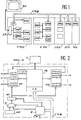
- Figure 1 shows schematically and as an example of application the central subsystem of a computer system composed of one or more cards CPU processor, one or more IOU I / O cards, a SCU memory controller, MU memory cards and a CMU maintenance card. These units are associated with a service processor SP connected to the maintenance card CMU, which is itself connected to the other units via a maintenance bus CMB.
- Each card for example one of the processor CPU cards, comprises several functional units BDP, EAD, FPP, DIR, DAT which can each be produced in the form of an integrated circuit. All the units of all the cards operate synchronously and communicate with each other by suitable functional links (bus for example) not shown.
- the functional units of each card are synchronized by an ARG clock signal generator mounted on the card and whose operation is controlled by the service processor via the CMB bus.
- the maintenance card CMU has a primary or master clock generator (hereinafter designated ARG-M) which supplies the secondary clock generators or slaves of the other cards with clock signals master via specific connections not shown.
- ARG-M master clock generator
- the CMU card comprises a microprocessor system mP associated with a random access memory RAM, a read only memory ROM, a unit for direct access to the memory DMA and interface circuits (IP, IF) with respectively the service processor SP and the CMB bus.
- mP microprocessor system
- mP associated with a random access memory RAM, a read only memory ROM, a unit for direct access to the memory DMA and interface circuits (IP, IF) with respectively the service processor SP and the CMB bus.
- the CMB bus is a microprocessor bus of conventional type comprising data, address and control lines, the detailed description of which is superfluous since it is well known in the microprocessor technique.
- This bus is connected to the functional units as well as to the clock generators of the cards so as to control the operations maintenance at the system level and in particular to control the initialization and adjustment of the clock signals.
- the clock system generally works as follows. On the initiative of the service processor SP, the microprocessor mP executes a specific firmware having in particular the result of placing on the bus CMB, via the interface IF, control signals intended for the various clock generators ARG. The detailed operation at the level of each clock generator will be explained with reference to FIG. 2.
- FIG. 2 represents the ARG-M clock generator as well as a non-volatile memory 1 of the maintenance card CMU.
- the ARG-M generator circuits can be subdivided into three main parts: a master part PM, a slave part PE and a synchronous part PS.
- the master part PM which includes a quartz oscillator (not shown) supplies master clock signals PHP1, PHP2 intended for the various cards of the system numbered 0, 1, ..., p, the CMU card carrying the number zero.
- the clock generators of the other units also include a synchronous part and a slave part receiving the master clock signals intended for them. From the master clock signals PHP1, PHP2, each clock generator generates, via its slave part, secondary or slave clock signals CK1, CK2 intended for the various integrated circuits of the card.
- the signals PHP1 (0), PHP2 (0) are sent to the slave part PE of the generator ARG-M of the card CMU. From these signals, PE provides the slave clock signals CK1 (0), CK2 (0), ..., CK1 (i), CK2 (i), ..., CK1 (n), CK2 (n ) intended respectively for integrated circuits numbered 0, ..., i, ..., n of the card in question.
- the signals CK1 (0), CK2 (0) are transmitted to the synchronous part PS of the generator.
- the shape of the signals PHP1, PHP2, CK1, CK2 is represented in FIG. 3.
- the signal PHP1 has a frequency twice of each of the signals CK1 and CK2 while the signal PHP2 is a signal of discrimination of these two phases.
- This example given purely by way of illustration is in the context of a two-phase operation CK1, CK2, the master clock shown having been chosen to increase the phase tolerance of the signals PHP1 and PHP2 taking into account the disturbances due to the links between the master clock generator and the slave clock generators of the different cards.
- the maintenance bus CMB is connected to the synchronous part PS via IO interface circuits used in particular for resynchronization of the signals exchanged between the microprocessor mP and the synchronous part PS because the microprocessor system is synchronized by an independent clock that of the system to be adjusted.
- the generator ARG-M includes an adjustment register RT, the output of which is connected to the adjustment inputs of the master and slave parts PM, PE so as to supply them with the respective adjustment values.
- the adjustment register RT is commanded in writing by a selection and writing circuit 2 connected as an input to the maintenance buses CMB.
- the input of the adjustment register RT is connected to the output of a multiplexer 3 controlled by the circuit 2.
- the multiplexer 3 has a first input connected to the data output of the circuit 2 and a second input receiving an engraved digital RF value in the substrate.
- the RF value is an approximate value corresponding to the setting to be applied if the generator and unit circuits have the most probable characteristics among those which can be obtained by the manufacturing process or processes chosen to produce these circuits.
- Circuit 2 finally receives a PW signal representative of a power-up of the system.
- the synchronous part PS includes a read and write interface connected to the non-volatile memory 1 by an appropriate link.
- the memory 1 can for example be produced by means of an electrically erasable programmable memory (EEPROM).
- EEPROM electrically erasable programmable memory
- this memory is of the serial type so as to reduce the number of links between this memory and the synchronous part PS.
- the synchronous part PS also includes circuits for decoding the addresses received from the CMB bus as well as a data path comprising a set of control registers, memory banks and automata to perform certain maintenance operations, the description of which exhaustive detailed would depart from the scope of the present invention.
- the PS part includes data transfer circuits between this memory and the CMB bus. All these circuits are synchronized by the clock signals CK1 (0), CK2 (0).
- the selection and write circuit 2 comprises a circuit for decoding the commands and addresses received from the CMB bus and circuits for generating as a function of these signals and of the power-on signal PW the selection signals of the multiplexer 3 and of command to write the adjustment register RT.
- Circuit 2 also includes a circuit for transferring data from the CMB bus to the input of multiplexer 3.
- Circuit 2 is an asynchronous logic circuit, the production of which by means of conventional logic gates can be easily deduced from the operation which will be described.
- slave clock generators are distinguished from ARG-M by the absence (or non-use) of the PM master part. Consequently, only the PE slave part of these generators is liable to be adjusted.
- the adjustment of the system clock generators is carried out in two phases: a preliminary phase of determining the optimal value of the adjustment parameters by placing each card of the system on a test bench, then an adjustment phase proper from of these optimal values, this second phase being executed each time the system is powered up after its installation.
- the operations are initialized by the service processor SP and executed under the control of corresponding firmware of the microprocessor system mP.
- the first adjustment phase takes place as follows.
- the microprocessor mP controls the circuit 2 via the CMB bus so that it authorizes, via the multiplexer 3, the transfer of data between the CMB bus and the adjustment register RT.
- mP then sends a series of values of the adjustment parameters which are loaded successively into the register RT until the characteristics of the clock signals coincide with reference characteristics.
- the optimal value of the adjustment parameters is then defined.
- mP calculates the detector code and error corrector (Hamming code for example) associated with this value optimal. Then, mP controls the synchronous part PS so that it writes the optimal value and its error code in memory 1.
- circuit 2 transfers the approximate value RF into the register RT.
- the PM and PE parts then provide approximate clock signals PHP1, PHP2, CK1, CK2.
- the synchronous part PS is then synchronized by the approximate clock signals CK1 (0), CK2 (0).
- the synchronous part PS then reads memory 1 and the value read is transmitted with its error code to the microprocessor mP.
- mP then performs an error detection operation and if no error is detected, it controls circuit 2 so that it loads this value into the register RT.
- mP If mP detects one or more errors that can be corrected using the code, it performs the correction and commands circuit 2 to load the corrected value into the register RT. mP then commands a new reading from memory 1 and checks the accuracy of the new value read. If the average RF value had been too far from the optimal value, the first reading of memory 1 would have been affected by too many errors to be corrected. In this case, mP executes an algorithm for searching for an initial setting value making it possible to obtain a reading that is at least correctable.
- mP loads the register RT first with an average value then with a value corresponding to an intermediate case between the most probable technology and the worst technology, then corresponding to an intermediate case between the most probable technology and the best technology, then the case corresponding to the best technology, then the case corresponding to the most bad technology.
- one of the previous tests leads to a correct or correctable reading of the value of the adjustment parameters.
- FIG. 4 represents the master part PM of the generator ARG-M of the card CMU.
- This circuit receives a basic clock signal H supplied by a quartz oscillator.
- the signal H is transmitted after amplification on the one hand to a first input of a shaping circuit 5 and on the other hand to the second input of circuit 5 via a delay line 4.
- the line 4 which is associated with an adaptation divider bridge is external to the PM part when the latter is produced in the form of an integrated circuit.
- the integrated circuit then has two terminals OSCA and OSCR for connecting the delay line to it.
- the shaping circuit 5 can be produced by means of a circuit equivalent to a flip-flop RS which supplies a PHP signal calibrated in width as a function of the characteristics of the delay line 4.
- the shape of the PHP signal is analogous to that of the PHP1 signal shown in Figure 3.
- the PHP signal is then applied to the input of a variable delay circuit 6 providing a first PHP1B output signal identical to the PHP signal and a second PHP2B signal obtained from the PHP signal after processing in a bistable circuit followed by a delay circuit controlled by the parameters RM.
- This delay circuit can be simply implemented by means of a chain of reversers selectively put in series according to the RM command to obtain the desired phase shift between PHP1B and PHP2B.
- Each PHP1B or PHP2B signal is then applied to the input of amplifiers CIB with adjustable impedance according to an IS setting value.
- Each CIB amplifier is assigned to a system card. For example, two amplifiers supply the signals PHP1 (j) and PHP2 (j) intended for the card j.
- circuit of Figure 4 The operation of the circuit of Figure 4 is easily deduced from the diagram. It may however be noted that the circuit offers the possibility of adjusting each amplifier CIB independently of the others to take account of the differences in characteristics of the circuits receiving the output signals of these amplifiers. In practice, for reasons of simplification of the adjustment and especially of the test operations, one can be satisfied with applying the same IS adjustment to all the amplifiers. In this case, only the manufacturing dispersions of the clock generator are corrected.
- FIG. 5 represents the slave part PE of the generators.
- This circuit receives the signals PHP1, PHP2 from corresponding amplifiers of the master generator. These signals are processed by a set of logic circuits supplying the signals CK1A and CK2A resulting respectively from the logical AND operation on the one hand between PHP1 and PHP2 and on the other hand between PHP1 and the complement of PHP2.
- the signals CK1A and CK2B have the appearance of the signals CK1 and CK2 in FIG. 3 respectively.
- the inverse signals E1, E2 respectively of CK1A, CK2A are then processed by a variable delay circuit 7 delivering two delayed signals Y1, Y2 according to the adjustment command RE.
- the detailed embodiment of circuit 7 will be given with reference to FIG. 8.
- the signals Y1 and Y2 are each applied to the input of a NOR gate so as to supply the signals CK1B and CK2B identical to the signals Y1 and Y2 when the doors NOR are validated by authorization signals applied to the second input of each of these doors.
- the signals CK1B and CK2B are then amplified by amplifiers CIB with adjustable impedance according to the IS-E tuning parameters to provide adjusted clock signals CK1 and CK2.
- FIG. 6 represents the block diagram of the amplifiers CIB in the case of their application to the primary generator.
- the amplifier consists essentially of several modules M1, M2, ..., M5 mounted in parallel and each receiving as input the clock signal to be set (PHP1B in the case of the example shown), after possibly validation by l 'through a logic gate controlled by a validation signal.
- Each module M1 to M5 is in fact an amplifier with 3 states controlled by one of the bits of the IS adjustment parameters and dimensioned so as to have a determined impedance.
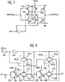
- FIG. 7 An exemplary CMOS embodiment of these modules is shown in FIG. 7. It is produced by means of 4 n-channel transistors: NA, ND, NC, NE and 4 p-channel transistors: PB, PH, PG, PF.
- the transistors PG and NC are connected in series between the positive voltage Vdd and the ground via the drain-source path of the transistor NE and receive on their gate the input signal PHP1B.
- the transistors PB and NA are connected in series between Vdd and the ground and their gates are connected respectively to the common point on the one hand with PG and NE and on the other hand with NC and NE.
- the transistors PH, PF and ND are respectively connected in parallel with the transistors PG, NE and NC.
- the gates of the PF and ND transistors are linked together and constitute the EN validation input of the module.
- EN constitutes the input of an inverter whose output is connected to the gates of the NE and PH transistors.
- the point common to PB and NA constitutes the output PHP1 (j) of the amplifier.
- the PHP1 (j) output is then in the high impedance state whatever the logical state of the PHP1B input.
- PB and NA constitute two inverters connected in cascade whose output PHP1 (j) reproduces the input PHP1B.
- the output impedance of each module is determined by the resistance of the drain-source paths of the transistors PB and NA which can be determined by dimensioning the width of these transistors.
- NA the resistance of the drain-source paths of the transistors PB and NA which can be determined by dimensioning the width of these transistors.
- the IS adjustment parameters will then be chosen so as to validate the modules whose paralleling has the appropriate impedance.
- variable delay circuit 7 can be produced in accordance with French patent application number 9010579, filed on August 23, 1990 and having for title "Circuit with adjustable time constant and application to an adjustable delay circuit" which must be considered as making part of this description.
- this circuit is produced by means of a plurality of modules conforming to FIG. 8, the points E, X and Y of which are connected together respectively, E constituting one of the inputs E1 or E2 while Y constitutes one of its outputs Y1 or Y2.
- Each module according to FIG. 8 is validated as a function of one of the bits RE (x) of the adjustment word RE.
Landscapes
- Engineering & Computer Science (AREA)
- Theoretical Computer Science (AREA)
- Physics & Mathematics (AREA)
- General Engineering & Computer Science (AREA)
- General Physics & Mathematics (AREA)
- Stabilization Of Oscillater, Synchronisation, Frequency Synthesizers (AREA)
- Tests Of Electronic Circuits (AREA)
- Information Transfer Systems (AREA)
- Dram (AREA)
Applications Claiming Priority (2)
| Application Number | Priority Date | Filing Date | Title |
|---|---|---|---|
| FR9010805 | 1990-08-30 | ||
| FR9010805A FR2666424B1 (fr) | 1990-08-30 | 1990-08-30 | Procede et dispositif de reglage des signaux d'horloge dans un systeme synchrone. |
Publications (2)
| Publication Number | Publication Date |
|---|---|
| EP0474541A1 true EP0474541A1 (de) | 1992-03-11 |
| EP0474541B1 EP0474541B1 (de) | 1999-06-09 |
Family
ID=9399956
Family Applications (1)
| Application Number | Title | Priority Date | Filing Date |
|---|---|---|---|
| EP91402322A Expired - Lifetime EP0474541B1 (de) | 1990-08-30 | 1991-08-28 | Verfahren und Vorrichtung zur Taktsignalregelung in einem Synchronsystem |
Country Status (5)
| Country | Link |
|---|---|
| US (1) | US5305453A (de) |
| EP (1) | EP0474541B1 (de) |
| JP (1) | JPH04256114A (de) |
| DE (1) | DE69131310T2 (de) |
| FR (1) | FR2666424B1 (de) |
Families Citing this family (14)
| Publication number | Priority date | Publication date | Assignee | Title |
|---|---|---|---|---|
| JPH05268016A (ja) * | 1992-02-19 | 1993-10-15 | Nec Corp | 半導体集積回路 |
| US5640523A (en) * | 1994-09-02 | 1997-06-17 | Cypress Semiconductor Corporation | Method and apparatus for a pulsed tri-state phase detector for reduced jitter clock recovery |
| JPH08123520A (ja) * | 1994-10-25 | 1996-05-17 | Mitsubishi Electric Corp | 駆動制御指令装置と複数台の駆動制御指令装置の同期制御システム及びその同期制御方法 |
| US5455540A (en) * | 1994-10-26 | 1995-10-03 | Cypress Semiconductor Corp. | Modified bang-bang phase detector with ternary output |
| FR2767935B1 (fr) * | 1997-09-04 | 1999-11-12 | Bull Sa | Procede pour synchroniser un systeme informatique et systeme informatique ainsi synchronise |
| US6304517B1 (en) | 1999-06-18 | 2001-10-16 | Telefonaktiebolaget Lm Ericsson (Publ) | Method and apparatus for real time clock frequency error correction |
| JP3880302B2 (ja) * | 2000-10-12 | 2007-02-14 | 富士通株式会社 | 位相合成回路およびタイミング信号発生回路 |
| US20020061107A1 (en) * | 2000-09-25 | 2002-05-23 | Tham Terry K. | Methods and apparatus for implementing a cryptography engine |
| US20020078342A1 (en) * | 2000-09-25 | 2002-06-20 | Broadcom Corporation | E-commerce security processor alignment logic |
| US6621882B2 (en) | 2001-03-02 | 2003-09-16 | General Dynamics Information Systems, Inc. | Method and apparatus for adjusting the clock delay in systems with multiple integrated circuits |
| US20030084360A1 (en) * | 2001-08-21 | 2003-05-01 | Grant David Alexander | Method of synchronizing and phase staggering two or more sampled data systems |
| US7372928B1 (en) | 2002-11-15 | 2008-05-13 | Cypress Semiconductor Corporation | Method and system of cycle slip framing in a deserializer |
| US8085857B1 (en) | 2003-09-25 | 2011-12-27 | Cypress Semiconductor Corporation | Digital-compatible multi-state-sense input |
| US10037213B2 (en) | 2016-09-19 | 2018-07-31 | Nxp Usa, Inc. | System and method for adjusting boot interface frequency |
Citations (3)
| Publication number | Priority date | Publication date | Assignee | Title |
|---|---|---|---|---|
| EP0294505A1 (de) * | 1987-06-11 | 1988-12-14 | International Business Machines Corporation | Taktgeneratorsystem |
| NL8802532A (nl) * | 1988-10-14 | 1990-05-01 | Philips Nv | Data-verwerkend systeem met klokpulsgenerator. |
| EP0366326A2 (de) * | 1988-10-28 | 1990-05-02 | Hewlett-Packard Company | Vorrichtung für ein Taktverteilungssystem mit geringer Taktverschiebung und Erzeugung von doppelfrequenten Taktsignalen |
Family Cites Families (11)
| Publication number | Priority date | Publication date | Assignee | Title |
|---|---|---|---|---|
| NL7014137A (de) * | 1970-09-25 | 1972-03-28 | ||
| US3809884A (en) * | 1972-11-15 | 1974-05-07 | Honeywell Inf Systems | Apparatus and method for a variable memory cycle in a data processing unit |
| FR2498035B1 (fr) * | 1981-01-09 | 1986-01-17 | Thomson Csf | Procede et dispositif de synchronisation de messages |
| US4509120A (en) * | 1982-09-30 | 1985-04-02 | Bell Telephone Laboratories, Inc. | Variable cycle-time microcomputer |
| US4637018A (en) * | 1984-08-29 | 1987-01-13 | Burroughs Corporation | Automatic signal delay adjustment method |
| JPH02501613A (ja) * | 1987-03-16 | 1990-05-31 | シーメンス、アクチエンゲゼルシヤフト | Mosトランジスタを有するゲート回路 |
| US5086500A (en) * | 1987-08-07 | 1992-02-04 | Tektronix, Inc. | Synchronized system by adjusting independently clock signals arriving at a plurality of integrated circuits |
| JPH02126311A (ja) * | 1988-11-04 | 1990-05-15 | Nec Ic Microcomput Syst Ltd | マイクロコンピュータ |
| US4989175A (en) * | 1988-11-25 | 1991-01-29 | Unisys Corp. | High speed on-chip clock phase generating system |
| US5028824A (en) * | 1989-05-05 | 1991-07-02 | Harris Corporation | Programmable delay circuit |
| US5036230A (en) * | 1990-03-01 | 1991-07-30 | Intel Corporation | CMOS clock-phase synthesizer |
-
1990
- 1990-08-30 FR FR9010805A patent/FR2666424B1/fr not_active Expired - Lifetime
-
1991
- 1991-08-28 DE DE69131310T patent/DE69131310T2/de not_active Expired - Fee Related
- 1991-08-28 US US07/750,967 patent/US5305453A/en not_active Expired - Lifetime
- 1991-08-28 EP EP91402322A patent/EP0474541B1/de not_active Expired - Lifetime
- 1991-08-30 JP JP3244881A patent/JPH04256114A/ja active Pending
Patent Citations (3)
| Publication number | Priority date | Publication date | Assignee | Title |
|---|---|---|---|---|
| EP0294505A1 (de) * | 1987-06-11 | 1988-12-14 | International Business Machines Corporation | Taktgeneratorsystem |
| NL8802532A (nl) * | 1988-10-14 | 1990-05-01 | Philips Nv | Data-verwerkend systeem met klokpulsgenerator. |
| EP0366326A2 (de) * | 1988-10-28 | 1990-05-02 | Hewlett-Packard Company | Vorrichtung für ein Taktverteilungssystem mit geringer Taktverschiebung und Erzeugung von doppelfrequenten Taktsignalen |
Also Published As
| Publication number | Publication date |
|---|---|
| US5305453A (en) | 1994-04-19 |
| JPH04256114A (ja) | 1992-09-10 |
| DE69131310T2 (de) | 1999-11-04 |
| EP0474541B1 (de) | 1999-06-09 |
| FR2666424A1 (fr) | 1992-03-06 |
| FR2666424B1 (fr) | 1992-11-06 |
| DE69131310D1 (de) | 1999-07-15 |
Similar Documents
| Publication | Publication Date | Title |
|---|---|---|
| EP0474541B1 (de) | Verfahren und Vorrichtung zur Taktsignalregelung in einem Synchronsystem | |
| US8008954B2 (en) | Multi-phase signal generator and method | |
| US8135555B2 (en) | Strobe-offset control circuit | |
| US6530006B1 (en) | System and method for providing reliable transmission in a buffered memory system | |
| US7954031B2 (en) | Method and apparatus for generating expect data from a captured bit pattern, and memory device using same | |
| JP6113215B2 (ja) | プログラマブルロジックデバイスにおける書き込みレベリングインプリメンテーション | |
| US6279090B1 (en) | Method and apparatus for resynchronizing a plurality of clock signals used in latching respective digital signals applied to a packetized memory device | |
| JP4634803B2 (ja) | データ取得の方法と装置 | |
| KR102674031B1 (ko) | 메모리 컨트롤러, 이를 포함하는 메모리 시스템 및 그 동작 방법 | |
| US8209560B2 (en) | Transmission system where a first device generates information for controlling transmission and latch timing for a second device | |
| KR20070026498A (ko) | 앞선 위상 등화를 이용한 dll 위상 검출 | |
| TW200427228A (en) | Digital delay locked loop and control method thereof | |
| FR2790887A1 (fr) | Circuit logique protege contre des perturbations transitoires | |
| US8988126B2 (en) | Apparatus and method for latency control in high frequency synchronous semiconductor device | |
| FR3066033A1 (fr) | Dispositif d'etage tampon, en particulier apte a etre connecte sur un bus du type interface de peripherique serie | |
| US7391255B2 (en) | Semiconductor phase adjustment system module | |
| EP0488893B1 (de) | Verfahren und Vorrichtung zur Übertragung binärer Differenzsignale und Verwendung in Carry-Select-Addierern | |
| CN118675570A (zh) | 时钟信号同步电路、其操作方法以及半导体存储器装置 | |
| US12294379B2 (en) | Clock generating circuit and semiconductor apparatus using the same | |
| FR2788353A1 (fr) | Microprocesseur avec circuits de protection pour securiser l'acces a ses registres | |
| FR2683060A1 (fr) | Circuit de commande de sortie de donnee. | |
| US7177229B2 (en) | Apparatus for tuning a RAS active time in a memory device | |
| EP3893117B1 (de) | Überprüfungsschaltkreis des inhalts von registern | |
| FR2903205A1 (fr) | Procede de controle du temps d'evaluation d'une machine d'etat | |
| US7319635B2 (en) | Memory system with registered memory module and control method |
Legal Events
| Date | Code | Title | Description |
|---|---|---|---|
| PUAI | Public reference made under article 153(3) epc to a published international application that has entered the european phase |
Free format text: ORIGINAL CODE: 0009012 |
|
| 17P | Request for examination filed |
Effective date: 19920107 |
|
| AK | Designated contracting states |
Kind code of ref document: A1 Designated state(s): DE ES FR GB GR IT NL SE |
|
| RAP3 | Party data changed (applicant data changed or rights of an application transferred) |
Owner name: BULL S.A. |
|
| RAP1 | Party data changed (applicant data changed or rights of an application transferred) |
Owner name: BULL S.A. |
|
| 17Q | First examination report despatched |
Effective date: 19970530 |
|
| GRAG | Despatch of communication of intention to grant |
Free format text: ORIGINAL CODE: EPIDOS AGRA |
|
| GRAG | Despatch of communication of intention to grant |
Free format text: ORIGINAL CODE: EPIDOS AGRA |
|
| GRAH | Despatch of communication of intention to grant a patent |
Free format text: ORIGINAL CODE: EPIDOS IGRA |
|
| RIN1 | Information on inventor provided before grant (corrected) |
Inventor name: BRINKHUYSEN, JACQUES Inventor name: BOUDRY, JEAN-MARIE |
|
| GRAH | Despatch of communication of intention to grant a patent |
Free format text: ORIGINAL CODE: EPIDOS IGRA |
|
| GRAA | (expected) grant |
Free format text: ORIGINAL CODE: 0009210 |
|
| AK | Designated contracting states |
Kind code of ref document: B1 Designated state(s): DE ES FR GB GR IT NL SE |
|
| PG25 | Lapsed in a contracting state [announced via postgrant information from national office to epo] |
Ref country code: IT Free format text: LAPSE BECAUSE OF FAILURE TO SUBMIT A TRANSLATION OF THE DESCRIPTION OR TO PAY THE FEE WITHIN THE PRESCRIBED TIME-LIMIT;WARNING: LAPSES OF ITALIAN PATENTS WITH EFFECTIVE DATE BEFORE 2007 MAY HAVE OCCURRED AT ANY TIME BEFORE 2007. THE CORRECT EFFECTIVE DATE MAY BE DIFFERENT FROM THE ONE RECORDED. Effective date: 19990609 Ref country code: GR Free format text: LAPSE BECAUSE OF NON-PAYMENT OF DUE FEES Effective date: 19990609 Ref country code: ES Free format text: THE PATENT HAS BEEN ANNULLED BY A DECISION OF A NATIONAL AUTHORITY Effective date: 19990609 Ref country code: SE Free format text: THE PATENT HAS BEEN ANNULLED BY A DECISION OF A NATIONAL AUTHORITY Effective date: 19990609 |
|
| GBT | Gb: translation of ep patent filed (gb section 77(6)(a)/1977) |
Effective date: 19990610 |
|
| REF | Corresponds to: |
Ref document number: 69131310 Country of ref document: DE Date of ref document: 19990715 |
|
| PLBE | No opposition filed within time limit |
Free format text: ORIGINAL CODE: 0009261 |
|
| STAA | Information on the status of an ep patent application or granted ep patent |
Free format text: STATUS: NO OPPOSITION FILED WITHIN TIME LIMIT |
|
| 26N | No opposition filed | ||
| REG | Reference to a national code |
Ref country code: GB Ref legal event code: IF02 |
|
| PGFP | Annual fee paid to national office [announced via postgrant information from national office to epo] |
Ref country code: GB Payment date: 20060801 Year of fee payment: 16 |
|
| PGFP | Annual fee paid to national office [announced via postgrant information from national office to epo] |
Ref country code: DE Payment date: 20060810 Year of fee payment: 16 |
|
| GBPC | Gb: european patent ceased through non-payment of renewal fee |
Effective date: 20070828 |
|
| PG25 | Lapsed in a contracting state [announced via postgrant information from national office to epo] |
Ref country code: DE Free format text: LAPSE BECAUSE OF NON-PAYMENT OF DUE FEES Effective date: 20080301 |
|
| PGFP | Annual fee paid to national office [announced via postgrant information from national office to epo] |
Ref country code: NL Payment date: 20080728 Year of fee payment: 18 |
|
| PG25 | Lapsed in a contracting state [announced via postgrant information from national office to epo] |
Ref country code: GB Free format text: LAPSE BECAUSE OF NON-PAYMENT OF DUE FEES Effective date: 20070828 |
|
| REG | Reference to a national code |
Ref country code: NL Ref legal event code: V1 Effective date: 20100301 |
|
| PG25 | Lapsed in a contracting state [announced via postgrant information from national office to epo] |
Ref country code: NL Free format text: LAPSE BECAUSE OF NON-PAYMENT OF DUE FEES Effective date: 20100301 |
|
| PGFP | Annual fee paid to national office [announced via postgrant information from national office to epo] |
Ref country code: FR Payment date: 20100910 Year of fee payment: 20 |