EP0473443B1 - Halbleiterlaser mit vergrabener Streifenstruktur - Google Patents
Halbleiterlaser mit vergrabener Streifenstruktur Download PDFInfo
- Publication number
- EP0473443B1 EP0473443B1 EP91307938A EP91307938A EP0473443B1 EP 0473443 B1 EP0473443 B1 EP 0473443B1 EP 91307938 A EP91307938 A EP 91307938A EP 91307938 A EP91307938 A EP 91307938A EP 0473443 B1 EP0473443 B1 EP 0473443B1
- Authority
- EP
- European Patent Office
- Prior art keywords
- stripe
- layer
- laser device
- semiconductor laser
- inp
- Prior art date
- Legal status (The legal status is an assumption and is not a legal conclusion. Google has not performed a legal analysis and makes no representation as to the accuracy of the status listed.)
- Expired - Lifetime
Links
- 239000004065 semiconductor Substances 0.000 title claims description 101
- 239000000758 substrate Substances 0.000 claims description 61
- 238000000034 method Methods 0.000 claims description 41
- 239000013078 crystal Substances 0.000 claims description 32
- 230000010355 oscillation Effects 0.000 claims description 14
- 238000005530 etching Methods 0.000 claims description 9
- 230000000903 blocking effect Effects 0.000 claims description 6
- 238000004519 manufacturing process Methods 0.000 claims description 6
- VYPSYNLAJGMNEJ-UHFFFAOYSA-N Silicium dioxide Chemical compound O=[Si]=O VYPSYNLAJGMNEJ-UHFFFAOYSA-N 0.000 description 20
- 238000005253 cladding Methods 0.000 description 20
- 229910001218 Gallium arsenide Inorganic materials 0.000 description 13
- 125000005842 heteroatom Chemical group 0.000 description 12
- 229910052681 coesite Inorganic materials 0.000 description 10
- 229910052906 cristobalite Inorganic materials 0.000 description 10
- 239000000377 silicon dioxide Substances 0.000 description 10
- 229910052682 stishovite Inorganic materials 0.000 description 10
- 229910052905 tridymite Inorganic materials 0.000 description 10
- 230000000052 comparative effect Effects 0.000 description 8
- 229910000980 Aluminium gallium arsenide Inorganic materials 0.000 description 7
- 238000003486 chemical etching Methods 0.000 description 6
- PNEYBMLMFCGWSK-UHFFFAOYSA-N aluminium oxide Inorganic materials [O-2].[O-2].[O-2].[Al+3].[Al+3] PNEYBMLMFCGWSK-UHFFFAOYSA-N 0.000 description 4
- 229910052593 corundum Inorganic materials 0.000 description 4
- 239000012535 impurity Substances 0.000 description 4
- 238000002347 injection Methods 0.000 description 4
- 239000007924 injection Substances 0.000 description 4
- 229910001845 yogo sapphire Inorganic materials 0.000 description 4
- QAOWNCQODCNURD-UHFFFAOYSA-N Sulfuric acid Chemical compound OS(O)(=O)=O QAOWNCQODCNURD-UHFFFAOYSA-N 0.000 description 3
- 239000011259 mixed solution Substances 0.000 description 3
- 230000003287 optical effect Effects 0.000 description 3
- 238000000206 photolithography Methods 0.000 description 3
- 125000004429 atom Chemical group 0.000 description 2
- 230000015572 biosynthetic process Effects 0.000 description 2
- 150000001875 compounds Chemical class 0.000 description 2
- 238000002109 crystal growth method Methods 0.000 description 2
- 230000003247 decreasing effect Effects 0.000 description 2
- 238000009792 diffusion process Methods 0.000 description 2
- 230000010365 information processing Effects 0.000 description 2
- 239000002184 metal Substances 0.000 description 2
- 229920002120 photoresistant polymer Polymers 0.000 description 2
- 238000001947 vapour-phase growth Methods 0.000 description 2
- 201000009310 astigmatism Diseases 0.000 description 1
- 238000010276 construction Methods 0.000 description 1
- 230000008878 coupling Effects 0.000 description 1
- 238000010168 coupling process Methods 0.000 description 1
- 238000005859 coupling reaction Methods 0.000 description 1
- 238000009826 distribution Methods 0.000 description 1
- 230000000694 effects Effects 0.000 description 1
- 238000005566 electron beam evaporation Methods 0.000 description 1
- 239000000835 fiber Substances 0.000 description 1
- 230000020169 heat generation Effects 0.000 description 1
- 238000012986 modification Methods 0.000 description 1
- 230000004048 modification Effects 0.000 description 1
- 230000002250 progressing effect Effects 0.000 description 1
- 239000000243 solution Substances 0.000 description 1
- 230000006641 stabilisation Effects 0.000 description 1
- 238000011105 stabilization Methods 0.000 description 1
- 239000000126 substance Substances 0.000 description 1
- 239000012808 vapor phase Substances 0.000 description 1
Images


Classifications
-
- H—ELECTRICITY
- H01—ELECTRIC ELEMENTS
- H01S—DEVICES USING THE PROCESS OF LIGHT AMPLIFICATION BY STIMULATED EMISSION OF RADIATION [LASER] TO AMPLIFY OR GENERATE LIGHT; DEVICES USING STIMULATED EMISSION OF ELECTROMAGNETIC RADIATION IN WAVE RANGES OTHER THAN OPTICAL
- H01S5/00—Semiconductor lasers
- H01S5/20—Structure or shape of the semiconductor body to guide the optical wave ; Confining structures perpendicular to the optical axis, e.g. index or gain guiding, stripe geometry, broad area lasers, gain tailoring, transverse or lateral reflectors, special cladding structures, MQW barrier reflection layers
- H01S5/22—Structure or shape of the semiconductor body to guide the optical wave ; Confining structures perpendicular to the optical axis, e.g. index or gain guiding, stripe geometry, broad area lasers, gain tailoring, transverse or lateral reflectors, special cladding structures, MQW barrier reflection layers having a ridge or stripe structure
- H01S5/227—Buried mesa structure ; Striped active layer
-
- H—ELECTRICITY
- H10—SEMICONDUCTOR DEVICES; ELECTRIC SOLID-STATE DEVICES NOT OTHERWISE PROVIDED FOR
- H10H—INORGANIC LIGHT-EMITTING SEMICONDUCTOR DEVICES HAVING POTENTIAL BARRIERS
- H10H20/00—Individual inorganic light-emitting semiconductor devices having potential barriers, e.g. light-emitting diodes [LED]
- H10H20/01—Manufacture or treatment
- H10H20/011—Manufacture or treatment of bodies, e.g. forming semiconductor layers
- H10H20/013—Manufacture or treatment of bodies, e.g. forming semiconductor layers having light-emitting regions comprising only Group III-V materials
-
- H—ELECTRICITY
- H01—ELECTRIC ELEMENTS
- H01S—DEVICES USING THE PROCESS OF LIGHT AMPLIFICATION BY STIMULATED EMISSION OF RADIATION [LASER] TO AMPLIFY OR GENERATE LIGHT; DEVICES USING STIMULATED EMISSION OF ELECTROMAGNETIC RADIATION IN WAVE RANGES OTHER THAN OPTICAL
- H01S5/00—Semiconductor lasers
- H01S5/20—Structure or shape of the semiconductor body to guide the optical wave ; Confining structures perpendicular to the optical axis, e.g. index or gain guiding, stripe geometry, broad area lasers, gain tailoring, transverse or lateral reflectors, special cladding structures, MQW barrier reflection layers
- H01S5/22—Structure or shape of the semiconductor body to guide the optical wave ; Confining structures perpendicular to the optical axis, e.g. index or gain guiding, stripe geometry, broad area lasers, gain tailoring, transverse or lateral reflectors, special cladding structures, MQW barrier reflection layers having a ridge or stripe structure
- H01S5/2201—Structure or shape of the semiconductor body to guide the optical wave ; Confining structures perpendicular to the optical axis, e.g. index or gain guiding, stripe geometry, broad area lasers, gain tailoring, transverse or lateral reflectors, special cladding structures, MQW barrier reflection layers having a ridge or stripe structure in a specific crystallographic orientation
-
- H—ELECTRICITY
- H01—ELECTRIC ELEMENTS
- H01S—DEVICES USING THE PROCESS OF LIGHT AMPLIFICATION BY STIMULATED EMISSION OF RADIATION [LASER] TO AMPLIFY OR GENERATE LIGHT; DEVICES USING STIMULATED EMISSION OF ELECTROMAGNETIC RADIATION IN WAVE RANGES OTHER THAN OPTICAL
- H01S5/00—Semiconductor lasers
- H01S5/30—Structure or shape of the active region; Materials used for the active region
- H01S5/32—Structure or shape of the active region; Materials used for the active region comprising PN junctions, e.g. hetero- or double- heterostructures
- H01S5/323—Structure or shape of the active region; Materials used for the active region comprising PN junctions, e.g. hetero- or double- heterostructures in AIIIBV compounds, e.g. AlGaAs-laser, InP-based laser
- H01S5/3235—Structure or shape of the active region; Materials used for the active region comprising PN junctions, e.g. hetero- or double- heterostructures in AIIIBV compounds, e.g. AlGaAs-laser, InP-based laser emitting light at a wavelength longer than 1000 nm, e.g. InP-based 1300 nm and 1500 nm lasers
- H01S5/32391—Structure or shape of the active region; Materials used for the active region comprising PN junctions, e.g. hetero- or double- heterostructures in AIIIBV compounds, e.g. AlGaAs-laser, InP-based laser emitting light at a wavelength longer than 1000 nm, e.g. InP-based 1300 nm and 1500 nm lasers based on In(Ga)(As)P
Definitions
- This invention relates to a buried stripe type semiconductor laser device and a method of producing a buried stripe type semiconductor laser device.
- semiconductor laser devices are widely used as light sources for various consumer electronics and industrial apparatuses in such applications as optical communications and information processing.
- device characteristics such as high output power, high efficiency, and highspeed modulation
- stabilization of the transverse oscillation mode is important, because it has a close relation with fiber coupling efficiency in optical communications and with optical beam astigmatism in information processing.
- semiconductor laser devices having the Fabry-Perot resonator structure are classified into several types, such as a gain waveguide type having a current confinement structure, a built-in refractive index waveguide type having transverse distribution in a refractive index perpendicular to the cavity length of the resonator, and a refractive index waveguide type in which the sides of the waveguide are buried.
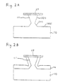
- a conventional buried stripe type semiconductor laser device having a buried hetero structure is shown in Figure 6.
- This buried stripe type semiconductor laser device can emit laser light oscillating stably in a single transverse mode at low threshold currents.
- the semiconductor laser device is fabricated in the following way.
- n-InP buffer layer 52, a GaInAsP active layer 53, a p-InP cladding layer 54, and a p-GaInAsP cap layer 55 are sequentially grown on an n-InP substrate 51 by a suitable crystal growth method (a first crystal growth process). Then, a stripe-shaped mesa portion (with a width of about 1 ⁇ m to 2 ⁇ m) is formed along the cavity length of the resonator by photolithography and chemical etching techniques.
- a p-InP first current stopping layer 56 and an n-InP second current stopping layer 57 are sequentially grown by a suitable crystal growth method in such a manner that the mesa portion is thereby buried (a second crystal growth process).
- an n-side electrode 58 is formed on the back of the n-InP substrate 51, and a p-side electrode 59 is formed on the top surfaces of the p-GaInAsP cap layer 55 and n-InP second current stopping layer 57, whereby the semiconductor laser device shown in Figure 6 can be obtained.
- FIG. 64-25590 Japanese Laid-Open Patent Publication No. 64-25590.
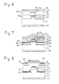
- Figure 7 shows a cross-sectional view of the buried stripe type semiconductor laser device. This semiconductor laser device is fabricated in the following way.
- a stripe-shaped mesa portion is formed on an n-GaAs substrate 61 having a main surface with a (100) crystal orientation, in the ⁇ 011> direction by using a suitable etching method.
- an n-GaAs film 62', an n-AlGaAs film 63', a GaAs film 64', and a p-AlGaAs film 65' are sequentially grown on the n-GaAs substrate 61, by a suitable method for crystal growth (e.g., metal organic vapor phase deposition method).
- a multilayer film consisting of an n-GaAs buffer layer 62, an n-AlGaAs first cladding layer 63, a GaAs active layer 64, and a p-AIGaAs second cladding layer 65 and surrounded by (111)B facets.
- an n-AlGaAs current stopping layer 66, a p-AlGaAs cladding layer 67, and a p-GaAs cap layer 68 are sequentially grown so as to bury the multilayer film.
- an n-side electrode 69 is formed on the back of the n-GaAs substrate 61, and a p-side electrode 70 is formed on the top surface of the p-GaAs cap layer 68, whereby the buried stripe type semiconductor laser device shown in Figure 7 can be obtained.
- the top surfaces of individual epitaxial layers grown sequentially over the semiconductor substrate rise along the stripe-shaped mesa portion. Such a tendency is more noticeable in the semiconductor laser devices using an InP substrate.
- the rate of crystal growth on the (111)B facets is substantially zero and, therefore, continuation of crystal growth after a multilayer film surrounded by the (111)B facets will result in an epitaxial growth progressing in such a way that the difference in level between the GaAs substrate and the mesa portion is reduced.
- the rate of crystal growth on the (111)B facets is considerably greater than in the case where the GaAs substrate is used and, therefore, epitaxial growth is continued while the level difference between the InP substrate and the mesa portion is held as it is.
- the resulting configuration will be as shown in figure 8.
- the buried stripe type semiconductor laser device shown in Figure 8 comprises an InP substrate 71 having a stripe-shaped ridge, a first multilayer film (including a cladding layer 72 and an active layer 73 formed on the cladding layer 72) formed on the top surface of the stripe-shaped ridge, a second multilayer film including layers 72' and 73' formed on the InP substrate 71, a cladding layer 74 for burying the multilayer films, a contact layer 75 formed on the cladding layer 74, an SiO 2 insulating layer 76 formed on the contact layer 75, a p-side electrode 78 formed on the SiO 2 insulating layer 76 and the contact layer 75, an n-side electrode 77 formed on the back of the InP substrate 71.
- the semiconductor laser device shown in Figure 8 is such that a portion above the mesa portion is in an uprising condition, the laser device cannot be mounted in position with the epitaxial layer side held down.
- the semiconductor laser device is often subject to thermal influences due to increased resistance to heat and, in addition, the mesa portion is susceptible to damage upon mounting of the device, with the result that some strain is generated in the active region, which leads to decreased reliability.
- the structure In order to stabilize the transverse oscillation mode and reduce the threshold current, it is necessary to provide a structure which can prevent the spread of injected currents so as to allow the electric currents to concentratively flow in a laser beam emitting active layer and can efficiently confine the laser lights in the narrow region.
- the structure In order to fabricate the buried stripe type semiconductor laser device in an easily reproducible manner and to obtain a high yield, the structure must be such that it can be constructed through a single crystal growth process. With semiconductor laser devices of such a structure, in order to define the region for current injection, there must be provided a stripe-shaped electrode or a stripe-shaped impurity diffused region.
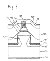
- Figure 9 shows a buried stripe type semiconductor laser device having the stripe-shaped impurity diffusion region disposed therein. This semiconductor laser device is fabricated in the following manner.
- a stripe-shaped ridge 131 is first formed on an n-InP substrate 130 having (100) surface, in [011] direction. Then, an n-InP film 132', a GaInAsP film 133', and a p-InP film 134' are sequentially grown on the n-InP substrate 130 on which the stripe-shaped ridge 131 is formed.
- This multilayer film consists of an n-InP first cladding layer 132, a GaInAsP active layer 133, and a p-InP second cladding layer 134.
- the p-InP film 134' grows to a thickness such that the p-InP film 134' does not go above the GaInAsP active layer 133 of the double hetero structure formed on the upper surface of the stripe-shaped ridge 131.
- InP crystal grows also on the (111)B facets of the multilayer film, therefore, as shown in Figure 9, the p-InP film 134' covers the multilayer film of the double hetero structure.
- an n-InP buried layer 135 and a P-GaInASP contact layer 136 are sequentially grown so as to bury the stripe-shaped ridge 131 covered with the p-InP film 134'.
- Zn is diffused in a stripe pattern so that it reaches the p-InP second cladding layer 134, in order to form a Zn diffused region 137 for current injection.
- an n-side electrode 138 is formed on the back of the n-InP substrate 130 and a p-side electrode 139 is formed on the surface of the p-GaInAsP contact layer 136.
- the n-InP film 132', GaInAsP film 133', and p-InP film 134' are formed on a plateau at both sides of the stripe-shaped ridge 131 as stated above. Therefore, in order for injection current to concentratively flow into the multilayer film of the double hetero structure formed on the top surface of the stripe-shaped ridge 131, the stripe-shaped Zn diffused region 137 was formed to extend from the p-side electrode 139 to the p-InP second cladding layer 134.
- the p-InP film 134' is grown also on the (111)B facet of the multilayer film, and this does not permit satisfactory current confinement by the p-n junction reverse bias generated in the burying layer. As a consequence, considerable current leaks through the p-InP film 134', which increases threshold currents.
- the preamble of claim 1 is based on the prior art laser shown in Figure 9 of this application.
- JP-A-63 73 690 discloses a semiconductor laser device having a mesa ridge.
- a current blocking layer is disposed over the surface of the substrate (except where the mesa ridge is provided), but does not entirely cover the sides of the mesa ridge.
- JP-A-60 116 185 discloses a semiconductor laser device having a mesa ridge.
- a current blocking layer is disposed over the surface of the substrate (except where the ridge is provided), but it does not extend for the entire height of the mesa ridge.
- JP-A-60 77 482 discloses a semiconductor laser device having a mesa ridge.
- a current blocking layer is disposed over the surface of the substrate (except where the ridge is provided), but again it does not extend for the entire height of the mesa ridge.
- a first aspect of the present invention provides a semiconductor laser device comprising:
- the current confinement means include a semiconductor layer of a second conductivity type formed on said main surface of said semiconductor substrate and side surfaces of said mesa stripe.
- the current confinement means include a semi-insulating semiconductor layer formed on said main surface of said semiconductor substrate and side surfaces of said mesa stripe.
- a second aspect of the present invention provides a method of fabricating a semiconductor laser device comprising the steps of:
- a stripe-shaped mesa portion is first formed on a semiconductor substrate of a first conductivity type having a (100) surface in the ⁇ 011> direction.
- the ⁇ 011> direction represents all directions which are crystallographically equivalent to the [011] direction and embraces, for example, the [01 1 ] direction.
- conventional photolithographic and etching techniques are employed for formation of the mesa portion.
- a multilayer film including a laser oscillating active layer, a cap layer of a second conductivity type, and an upper semiconductor layer are sequentially formed on the substrate with the mesa portion.
- the multilayer film is grown on the mesa portion in such a way that it has ⁇ 111 ⁇ facets.
- a ⁇ 111 ⁇ facet represents all crystal surfaces which are crystallographically equivalent to the (111) facet, including, for example, a (111)B facet.
- a buffer layer or a cladding layer may be formed at suitable locations as required.
- conventional crystal growing techniques including a metal organic chemical vapor phase deposition (MOCVD) method for example, are employed.
- Figure 1 is a cross-sectional view of an embodiment of the present invention.
- Figures 2A and 2B are cross-sectional views illustrating the process sequence of fabricating the device of Figure 1.
- Figure 3 is a cross-sectional view of a comparative example.
- Figures 4A through 4C are cross-sectional views illustrating the process sequence of fabricating the device of Figure 3.
- Figure 5 is a cross-sectional view of a comparative example.
- Figures 6 through 9 are cross-sectional views illustrating prior arts.
- Figure 1 shows a cross-sectional view of an embodiment of the invention.
- a semi-insulating current confinement layer is used as current confinement means.
- This semiconductor laser device was fabricated according to the following procedure.
- a photoresist was coated on an n-InP substrate 110 having a main surface with a (100) crystal orientation (n-InP (100) substrate 110), and a stripe-shaped opening extending in the [011] direction was formed in the photoresist by using a 4 ⁇ m wide mask pattern.
- An Al 2 O 3 film 250nm thick was formed all over the n-InP substrate 110 by an electron beam evaporation method, and then a stripe-shaped Al 2 O 3 mask 117 having a width of 4 ⁇ m was formed by a lift-off technique.
- each of side faces of the stripe-shaped ridge 111 comprises a ⁇ 221 ⁇ facet and a ⁇ 111 ⁇ facet.
- an Fe-doped InP layer (current blocking layer) 114 (having a thickness of about 0.5 ⁇ m on plateau regions at both sides of the stripe-shaped ridge 111) was grown by an MOCVD method, with the stripe-shaped Al 2 O 3 mask 117 left as such.
- the Fe-doped InP layer 114 was grown on both the ⁇ 221 ⁇ facets and the ⁇ 111 ⁇ facets of the stripe-shaped ridge 111, the rate of growth on the ⁇ 111 ⁇ facets being smaller than that on the ⁇ 221 ⁇ facets.
- the ⁇ 111 ⁇ facet was located between the ⁇ 221 ⁇ facet and the (100) surface, and was relatively small in area.
- n-InP substrate 110 having the current confinement structure were sequentially grown a Si-doped n-InP film 112' (with a thickness of 0.5 ⁇ m on the plateau) and a non-doped GaInAsP film 113' (with a thickness of 0.2 ⁇ m on the plateau) by a Low-Pressure MOCVD method.
- a Si-doped n-InP film 112' (with a thickness of 0.5 ⁇ m on the plateau)
- a non-doped GaInAsP film 113' with a thickness of 0.2 ⁇ m on the plateau
- the slant surfaces of the multilayer film were the (111)B facets grown from the both ends of the stripe-shaped ridge 111.
- This multilayer film consisted of an Si-doped n-InP buffer layer 112 (carrier concentration: 1 x 10 18 cm -3 ), and a non-doped GaInAsP active layer 113 (wavelength of emitted light: 1.3 ⁇ m).
- a Zn-doped p-InP cladding layer 115 carrier concentration: 5 x 10 17 cm -3 , 2.5 ⁇ m in thickness on the plateau regions
- a Zn-doped p-GaInAsP contact layer 116 carrier concentration: 1 x 10 18 cm -3 , 0.5 ⁇ m in thickness at the plateau
- the growth of GaInAsP crystal occurred only on the (100) surface because of the dependence of growth rate upon surface orientation, whereas the growth of InP crystal occurred not only on the (100) surface, but also on the (111)B facets, though the rate of crystal growth on the (111)B facets was less than one tenth of that on the (100) surface. Therefore, the multilayer of the double hetero structure was grown to form a trapezoidal sectional configuration perpendicular to the cavity length of the resonator, according to the dependence of crystal growth rate upon surface orientation.
- a multilayer film of similar construction was also grown on the (100) surface at both sides of the stripe-shaped ridge 111.
- the rate of crystal growth became uniform on all of the surfaces including the (111)B facets, and the multilayer film of the double hetero structure formed on the top of the stripe-shaped ridge 111 was buried by the Zn-doped p-InP cladding layer 115.
- the angle between side faces of the multilayer film on the stripe-shaped ridge 111 and the bottom face of the multilayer film corresponds to an angle between a (100) face and a (111)B face.
- the angle was crystallographically kept at about 54.7 degree.
- an n-side AuGe electrode 118 was formed on the back of the n-InP substrate 110, and a p-side AuZn electrode 119 on the surface of the Zn-doped p-GaInAsP contact layer 116.
- the buried stripe type semiconductor laser device shown in Figure 1 was obtained.
- the multilayer film of the double hetero structure including the non-doped GaInAsP active layer 113 was selectively grown by utilizing the Low-Pressure MOCVD technique. Therefore, the width of the active layer was easily set at about 2 ⁇ m with good accuracy and in an easily reproducible manner. Further, the current confinement structure using the high-resistance Fe-doped InP layer 114 was previously formed on the n-InP substrate 110, and accordingly the buried stripe type semiconductor laser device was easily obtained simply by burying both sides of the stripe-shaped ridge 111 in the Zn-doped p-InP cladding layer 115. Therefore, the semiconductor laser device exhibits steady oscillation in the single transverse mode and excellent device characteristics, such as a decreased leakage current and a low threshold current.
- the Fe-doped InP layer 114 was used as the semi-insulating current confinement layer.
- a semiconductor layer of a different conductivity type from that of the semiconductor substrate can be used as the current confinement layer.
- a p-type semiconductor layer which is of a different conductivity type from that of the n-InP substrate 110 may be used.
- the conductivity type of the semiconductor substrate or first conductivity type
- the conductivity type of the current confinement layer or second conductivity type
- the Low-Pressure MOCVD technique was employed for forming the current confinement structure on the n-InP substrate 110 and for growing the multilayer film of the double hetero structure including the non-doped GaInAsP active layer 113.
- an Atomospheric-Pressure MOCVD or a vapor phase epitaxial growth (VPE), or a molecular beam epitaxial growth (MBE) technique may be employed.
- the [011] direction was selected, but a [01 1 ] direction (a crystallographically equivalent direction) may be selected to obtain a similar result.
- the buried stripe type semiconductor laser device was of the InP-GaInAsP type.
- GaAs-AlGaAs and other compound semiconductors including multi-mixed crystal systems may be used for the buried stripe type semiconductor laser device of the invention, with similar excellent results.
- an active layer of a narrow width can be formed in a well reproducible manner in the manufacture of a buried stripe type semiconductor laser device.
- leakage currents can be reduced without forming any stripe-shaped region doped with impurity atoms in the burying layers. Therefore, it is possible to obtain a buried stripe type semiconductor laser device which reduces a threshold current level and attains a stable oscillation in single transverse mode, and which can be fabricated with good yield.
- Figure 3 shows a cross-sectional view of a comparative example of a buried stripe type semiconductor laser device according to the invention.
- the buried stripe type semiconductor laser device was fabricated in the following way.
- an SiO 2 film 21 (see Figure 4A) was deposited on an n-InP substrate 11 having a main surface with a (100) crystal orientation. Then, the SiO 2 film 21 was selectively etched by photolithography and chemical etching techniques using HF to form a stripe-shaped etching mask extending in the [011] direction. Next, the n-InP substrate 11 was selectively etched by a chemical etching method using a mixed solution of H 2 SO 4 , H 2 O 2 and H 2 O (3 : 1 : 1), whereby an inverse mesa ridge (1.8 ⁇ m high, 3 ⁇ m wide) was formed as shown in Figure 4A.
- an n-InP film 12' (0.7 ⁇ m thick), and a Ga 0.24 In 0.76 As 0.55 P 0.45 film 13' (0.1 ⁇ m thick) were sequentially grown over the n-InP substrate 11 by an MOCVD method.
- a multilayer film of a double hetero structure having a section of a trapezoidal configuration perpendicular to the cavity length of the resonator and surrounded by the (111)B facets. That is, the slant faces of the multilayer film are the (111)B facets.
- This multilayer film consists of an n-InP buffer layer 12 and a Ga 0.24 In 0.76 As 0.55 P 0.45 active layer 13.
- a p-InP cladding layer 14 (2.0 ⁇ m thick), a p-Ga 0.53 In 0.47 As cap layer 15 (0.5 ⁇ m thick), and an n-InP upper semiconductor layer 16 (1.8 ⁇ m thick) were sequentially grown.
- crystal growth progresses at both sides of the mesa portion, crystal growth occurred at a uniform rate on all the surfaces including the (111)B facets and thus a buried stripe type structure shown in Figure 4B was obtained.
- the raised portion of the n-InP upper semiconductor layer 16 above the mesa portion was selectively removed by the photolithography and chemical etching techniques, so that the surface above the mesa portion was made even with the surface at both sides thereof.
- a mixed solution of HCl and H 2 O (4 : 1) was used as an etchant, whereby the n-InP upper semiconductor layer 16 only could be selectively etched without etching the p-Ga 0.53 In 0.47 As cap layer 15.
- an SiO 2 insulating film 17 was deposited all over; and after the stripe portion of the SiO 2 insulating film 17 which would serve as a current injection region was removed by etching, an n-side electrode 18 was formed on the back of the n-InP substrate 11; and a p-side electrode 19 was formed on the surface of the SiO 2 insulating film 17 and on the surface of the P-Ga 0.53 In 0.47 As cap layer 15 exposed to the stripe portion of the film 17.
- the buried stripe type semiconductor laser device shown in Figure 3 was obtained.
- Another buried stripe type semiconductor laser device was fabricated in the same manner as described above, except that the inverse mesa ridge had a smaller width of the order of 1.5 ⁇ m.
- the buried stripe type semiconductor laser device was equally reproducible.
- the semiconductor laser device thus fabricated had a surface above the mesa portion which was even with or lower than the surface at both sides thereof, and was mounted in position with the epitaxial layer side down.
- the device was far much less liable to any thermal influence, such as temperature rise due to heat generation, and exhibited satisfactory device characteristics.
- Figure 5 shows a cross-sectional view of a further comparative example of a buried stripe type semiconductor laser device.
- the buried stripe type semiconductor laser device was fabricated in the following way.
- an inverse mesa ridge (1.8 ⁇ m high, 3 ⁇ m wide) was formed on an n-InP substrate 31 having a (100) surface in the same manner as in Example 2. Then, on the n-InP substrate 31 with the mesa portion were sequentially grown an n-InP film 32' (0.7 ⁇ m thick), and a Ga 0.24 In 0.76 As 0.55 P 0.45 film 33' (0.1 ⁇ m thick) in the same manner as in Example 2 using the MOCVD method. In this step, on the mesa portion was formed a multilayer film of a double hetero structure having a section of a trapezoidal configuration perpendicular to the cavity length of the resonator and surrounded by (111)B facets.
- the slant faces of the multilayer film were the (111)B facets grown from both edges of the mesa portion.
- This multilayer film consists of an n-InP buffer layer 32 and a Ga 0.24 In 0.76 As 0.55 P 0.45 active layer 33.
- a p-InP cladding layer 34 (1.0 ⁇ m thick), an n-InP current stopping layer 35 (0.5 ⁇ m thick), a p-InP cladding layer 36 (1.0 ⁇ m thick), a p-Ga 0.53 In 0.47 As cap layer 37 (0.5 ⁇ m thick), and an n-InP upper semiconductor layer 38 (1.8 ⁇ m thick) were sequentially grown to bury the multilayer film.
- the raised portion of the n-InP upper semiconductor layer 38 above the mesa portion was selectively removed by the photolithographic and chemical etching techniques, so that the surface above the mesa portion was made even with the surface at both sides thereof.
- a mixed solution of HCl and H 2 O (4 : 1) was used as an etchant.
- an SiO 2 insulating film 39 was deposited all over and, after the stripe portion thereof was removed by etching to form a stripe window in the SiO 2 insulating film 39, Zn was diffused through the stripe window to form a Zn-diffused region 40 in the burying layers. Further, the conductivity type of that portion of the n-InP current stopping layer 35 which was located above the mesa portion was inverted into p-type, and an n-side electrode 41 was formed on the back of the n-InP substrate 31, and a p-side electrode 42 was formed on the surface of the SiO 2 insulating film 39 and on the Zn-diffused region 40 which was exposed to the stripe portion of the insulating film 39. Thus, the buried stripe type semiconductor laser device shown in Figure 5 was obtained.
- the semiconductor laser device was provided with an n-InP current stopping layer 35.
- the conductivity type of that portion of the current stopping layer 35 which was located above the mesa portion was inverted into p-type by Zn diffusion. Therefore, by virtue of a p-n junction, injected currents can be confined more accurately, and thus the threshold current level can be further reduced.
- the conductivity type of the semiconductor substrate i.e., first conductivity type
- the conductivity type of the cap layer i.e., second conductivity type
- the first conductivity type is p-type
- the second conductivity type is n-type.
- the [011] direction was selected.
- the [01 1 ] direction which is crystallographically equivalent may be selected, with similar effects being obtainable.
- the buried stripe type semiconductor laser device was of the InP-GaInAsP type.
- the method of the invention is equally applicable to GaAs-AlGaAs and other compound semiconductors including multi-mixed crystal systems, with similar satisfactory results.
Landscapes
- Physics & Mathematics (AREA)
- Geometry (AREA)
- Condensed Matter Physics & Semiconductors (AREA)
- General Physics & Mathematics (AREA)
- Electromagnetism (AREA)
- Optics & Photonics (AREA)
- Semiconductor Lasers (AREA)
Claims (4)
- Halbleiterlaser mit:einem Halbleitersubstrat (110) von erstem Leitungstyp mit einer Hauptfläche mit der Kristallausrichtung (100);einem auf der Hauptfläche des Halbleitersubstrats (110) hergestellten Mesastreifen (111), der entlang der Richtung <011> ausgerichtet ist und eine Oberfläche mit der Kristallausrichtung (100) aufweist, und der durch einen Teil des Halbleitersubstrats (110) gebildet ist;einer auf der Oberfläche des Mesastreifens (111) hergestellten Mehrschichtstruktur mit einer aktiven Schicht (113) für Laserschwingung, wobei die Seitenflächen der Mehrschichtstruktur {111}-Flächen sind;dadurch gekennzeichnet, dass er ferner eine Stromeingrenzungseinrichtung (114) zum Eingrenzen elektrischer Ströme auf innerhalb den Mesastreifen (111) aufweist, die auf der Hauptfläche des Halbleitersubstrats (110) und an den gesamten Seitenflächen des Mesastreifens (111) ausgebildet ist.
- Halbleiterlaser nach Anspruch 1, bei dem die Stromeingrenzungseinrichtung (114) eine Halbleiterschicht von zweitem Leitungstyp aufweist, die auf der Hauptfläche des Halbleitersubstrats und an den Seitenflächen des Mesastreifens (111) ausgebildet ist.
- Halbleiterlaser nach Anspruch 1, bei dem die Stromeingrenzungseinrichtung (114) eine halbisolierende Halbleiterschicht aufweist, die auf der Hauptfläche des Halbleitersubstrats (110) und an den Seitenflächen des Mesastreifens (111) ausgebildet ist.
- Verfahren zum Herstellen eines Halbleiterlasers, das die folgenden Schritte aufweist:Herstellen eines Mesastreifens (111) auf einem Halbleitersubstrat (110) von erstem Leitungstyp, das über die Kristallausrichtung (100) verfügt, durch ein selektives Ätzverfahren unter Verwendung einer streifenförmigen Maske, wobei der Mesastreifen (111) entlang der Richtung <011> ausgerichtet ist und eine Oberfläche mit der Kristallausrichtung (100) aufweist;Herstellen einer Stromsperrschicht (114) auf der Hauptfläche des Halbleitersubstrats (110) und an den gesamten Seitenflächen des Mesastreifens (111) durch ein selektives Aufwachsverfahren unter Verwendung der streifenförmigen Maske;Entfernen der streifenförmigen Maske;Herstellen einer Mehrschichtstruktur auf der Oberfläche des Mesastreifens (111), die eine aktive Schicht (113) für Laserschwingung aufweist, wobei die Seitenflächen der Mehrschichtstruktur {111}-Flächen sind;Herstellen einer Halbleiterschicht (115) von zweitem Leitungstyp, um die Mehrschichtstruktur zu bedecken; undHerstellen einer Kontaktschicht (116) auf der Halbleiterschicht (115).
Applications Claiming Priority (4)
| Application Number | Priority Date | Filing Date | Title |
|---|---|---|---|
| JP229961/90 | 1990-08-30 | ||
| JP2229961A JP2708949B2 (ja) | 1990-08-30 | 1990-08-30 | 半導体レーザ装置の製造方法 |
| JP24171590A JPH04120788A (ja) | 1990-09-11 | 1990-09-11 | 半導体レーザ装置 |
| JP241715/90 | 1990-09-11 |
Publications (3)
| Publication Number | Publication Date |
|---|---|
| EP0473443A2 EP0473443A2 (de) | 1992-03-04 |
| EP0473443A3 EP0473443A3 (en) | 1993-03-03 |
| EP0473443B1 true EP0473443B1 (de) | 1999-03-24 |
Family
ID=26529082
Family Applications (1)
| Application Number | Title | Priority Date | Filing Date |
|---|---|---|---|
| EP91307938A Expired - Lifetime EP0473443B1 (de) | 1990-08-30 | 1991-08-30 | Halbleiterlaser mit vergrabener Streifenstruktur |
Country Status (3)
| Country | Link |
|---|---|
| US (1) | US5335241A (de) |
| EP (1) | EP0473443B1 (de) |
| DE (1) | DE69131034T2 (de) |
Families Citing this family (10)
| Publication number | Priority date | Publication date | Assignee | Title |
|---|---|---|---|---|
| JP2754957B2 (ja) * | 1991-07-10 | 1998-05-20 | 日本電気株式会社 | 半導体光制御素子およびその製造方法 |
| JP2823476B2 (ja) * | 1992-05-14 | 1998-11-11 | 三菱電機株式会社 | 半導体レーザおよびその製造方法 |
| FR2805619B1 (fr) * | 2000-02-24 | 2003-01-17 | Cit Alcatel | Composant optique comportant un guide a structure "ridge" grave chimiquement et son procede de fabrication |
| US6556605B1 (en) | 2000-02-29 | 2003-04-29 | Triquent Technology Holding, Co. | Method and device for preventing zinc/iron interaction in a semiconductor laser |
| US6664605B1 (en) * | 2000-03-31 | 2003-12-16 | Triquint Technology Holding Co. | Dopant diffusion blocking for optoelectronic devices using InAlAs and/or InGaAlAs |
| US7135411B2 (en) * | 2004-08-12 | 2006-11-14 | Northrop Grumman Corporation | Method for etching mesa isolation in antimony-based compound semiconductor structures |
| JP2013149724A (ja) * | 2012-01-18 | 2013-08-01 | Sumitomo Electric Ind Ltd | 光集積素子の製造方法 |
| JP5880065B2 (ja) | 2012-01-18 | 2016-03-08 | 住友電気工業株式会社 | 光集積素子の製造方法 |
| JP5880063B2 (ja) * | 2012-01-18 | 2016-03-08 | 住友電気工業株式会社 | 光集積素子の製造方法 |
| CN112635623A (zh) * | 2020-12-22 | 2021-04-09 | 度亘激光技术(苏州)有限公司 | 一种半导体器件的衬底结构及其制备方法 |
Citations (1)
| Publication number | Priority date | Publication date | Assignee | Title |
|---|---|---|---|---|
| JPH02156588A (ja) * | 1988-12-08 | 1990-06-15 | Matsushita Electric Ind Co Ltd | 半導体レーザおよびその製造方法 |
Family Cites Families (8)
| Publication number | Priority date | Publication date | Assignee | Title |
|---|---|---|---|---|
| JPS5367389A (en) * | 1976-11-29 | 1978-06-15 | Hitachi Ltd | Production of semiconductor laser |
| JPS6077482A (ja) * | 1983-10-04 | 1985-05-02 | Nec Corp | 半導体レ−ザの製造方法 |
| JP2716693B2 (ja) * | 1985-02-08 | 1998-02-18 | ソニー株式会社 | 半導体レーザー |
| FR2581801B1 (fr) * | 1985-05-13 | 1987-06-26 | Devoldere Pascal | Procede de realisation de lasers a semiconducteurs a jonctions bloquantes assurant un confinement electrique |
| JPS6425590A (en) * | 1987-07-22 | 1989-01-27 | Matsushita Electric Industrial Co Ltd | Manufacture of semiconductor laser |
| JPH0646669B2 (ja) * | 1987-07-28 | 1994-06-15 | 日本電気株式会社 | 半導体レ−ザ及びその製造方法 |
| JPH01283890A (ja) * | 1988-05-10 | 1989-11-15 | Mitsubishi Electric Corp | 半導体レーザ装置 |
| US5020510A (en) * | 1989-01-10 | 1991-06-04 | Jones Darrell R | Method and apparatus for heating the ground, roads or the like |
-
1991
- 1991-08-30 US US07/751,923 patent/US5335241A/en not_active Expired - Lifetime
- 1991-08-30 EP EP91307938A patent/EP0473443B1/de not_active Expired - Lifetime
- 1991-08-30 DE DE69131034T patent/DE69131034T2/de not_active Expired - Fee Related
Patent Citations (1)
| Publication number | Priority date | Publication date | Assignee | Title |
|---|---|---|---|---|
| JPH02156588A (ja) * | 1988-12-08 | 1990-06-15 | Matsushita Electric Ind Co Ltd | 半導体レーザおよびその製造方法 |
Also Published As
| Publication number | Publication date |
|---|---|
| EP0473443A2 (de) | 1992-03-04 |
| DE69131034D1 (de) | 1999-04-29 |
| US5335241A (en) | 1994-08-02 |
| EP0473443A3 (en) | 1993-03-03 |
| DE69131034T2 (de) | 1999-09-16 |
Similar Documents
| Publication | Publication Date | Title |
|---|---|---|
| EP0433051B1 (de) | Halbleiterlaser und Verfahren zur Herstellung desselben | |
| CA1151275A (en) | Semiconductor laser device and method of manufacturing the same | |
| EP0503211B1 (de) | Halbleiteranordnung mit einer auf einem strukturierten Substrat aufgewachsenen Schichtstruktur | |
| EP0272096B1 (de) | Halbleiterlaser | |
| US4948753A (en) | Method of producing stripe-structure semiconductor laser | |
| US5636237A (en) | Semiconductor laser device which makes it possible to realize high-speed modulation | |
| US4121179A (en) | Semiconductor injection laser | |
| US6512783B1 (en) | Semiconductor laser and method of manufacturing the same | |
| US4675710A (en) | Light emitting semiconductor device | |
| US5913107A (en) | Photosemiconductor device and method of fabricating the same | |
| EP0473443B1 (de) | Halbleiterlaser mit vergrabener Streifenstruktur | |
| JPH0332080A (ja) | 半導体発光素子およびその製造方法 | |
| US4764246A (en) | Buried undercut mesa-like waveguide and method of making same | |
| EP0209387B1 (de) | Halbleiterlaser-Vorrichtung | |
| US6556605B1 (en) | Method and device for preventing zinc/iron interaction in a semiconductor laser | |
| US4725112A (en) | Buried undercut mesa-like waveguide | |
| EP0264225B1 (de) | Halbleiterlaservorrichtung und Verfahren zur Herstellung derselben | |
| US5441912A (en) | Method of manufacturing a laser diode | |
| US5149670A (en) | Method for producing semiconductor light emitting device | |
| EP0321294B1 (de) | Halbleiterlaservorrichtung | |
| US7305017B2 (en) | Semiconductor optical device | |
| EP0298778B1 (de) | Halbleiterlaservorrichtungen und Verfahren zur Herstellung derselben | |
| CA1282874C (en) | Semiconductor devices employing high resistivity in p-based epitaxial layer forcurrent confinement | |
| Yoshikawa et al. | A novel technology for formation of a narrow active layer in buried heterostructure lasers by single-step MOCVD | |
| US4731791A (en) | Buried hetero-structure laser diode |
Legal Events
| Date | Code | Title | Description |
|---|---|---|---|
| PUAI | Public reference made under article 153(3) epc to a published international application that has entered the european phase |
Free format text: ORIGINAL CODE: 0009012 |
|
| AK | Designated contracting states |
Kind code of ref document: A2 Designated state(s): DE FR GB |
|
| PUAL | Search report despatched |
Free format text: ORIGINAL CODE: 0009013 |
|
| AK | Designated contracting states |
Kind code of ref document: A3 Designated state(s): DE FR GB |
|
| 17P | Request for examination filed |
Effective date: 19930712 |
|
| 17Q | First examination report despatched |
Effective date: 19931019 |
|
| GRAG | Despatch of communication of intention to grant |
Free format text: ORIGINAL CODE: EPIDOS AGRA |
|
| GRAG | Despatch of communication of intention to grant |
Free format text: ORIGINAL CODE: EPIDOS AGRA |
|
| GRAG | Despatch of communication of intention to grant |
Free format text: ORIGINAL CODE: EPIDOS AGRA |
|
| GRAH | Despatch of communication of intention to grant a patent |
Free format text: ORIGINAL CODE: EPIDOS IGRA |
|
| GRAH | Despatch of communication of intention to grant a patent |
Free format text: ORIGINAL CODE: EPIDOS IGRA |
|
| GRAA | (expected) grant |
Free format text: ORIGINAL CODE: 0009210 |
|
| AK | Designated contracting states |
Kind code of ref document: B1 Designated state(s): DE FR GB |
|
| REF | Corresponds to: |
Ref document number: 69131034 Country of ref document: DE Date of ref document: 19990429 |
|
| ET | Fr: translation filed | ||
| PLBE | No opposition filed within time limit |
Free format text: ORIGINAL CODE: 0009261 |
|
| STAA | Information on the status of an ep patent application or granted ep patent |
Free format text: STATUS: NO OPPOSITION FILED WITHIN TIME LIMIT |
|
| 26N | No opposition filed | ||
| REG | Reference to a national code |
Ref country code: GB Ref legal event code: IF02 |
|
| PGFP | Annual fee paid to national office [announced via postgrant information from national office to epo] |
Ref country code: DE Payment date: 20070823 Year of fee payment: 17 |
|
| PGFP | Annual fee paid to national office [announced via postgrant information from national office to epo] |
Ref country code: GB Payment date: 20070829 Year of fee payment: 17 |
|
| PGFP | Annual fee paid to national office [announced via postgrant information from national office to epo] |
Ref country code: FR Payment date: 20070808 Year of fee payment: 17 |
|
| GBPC | Gb: european patent ceased through non-payment of renewal fee |
Effective date: 20080830 |
|
| REG | Reference to a national code |
Ref country code: FR Ref legal event code: ST Effective date: 20090430 |
|
| PG25 | Lapsed in a contracting state [announced via postgrant information from national office to epo] |
Ref country code: FR Free format text: LAPSE BECAUSE OF NON-PAYMENT OF DUE FEES Effective date: 20080901 Ref country code: DE Free format text: LAPSE BECAUSE OF NON-PAYMENT OF DUE FEES Effective date: 20090303 |
|
| PG25 | Lapsed in a contracting state [announced via postgrant information from national office to epo] |
Ref country code: GB Free format text: LAPSE BECAUSE OF NON-PAYMENT OF DUE FEES Effective date: 20080830 |