EP0473365B1 - Differenzeingangsschaltung - Google Patents
Differenzeingangsschaltung Download PDFInfo
- Publication number
- EP0473365B1 EP0473365B1 EP91307741A EP91307741A EP0473365B1 EP 0473365 B1 EP0473365 B1 EP 0473365B1 EP 91307741 A EP91307741 A EP 91307741A EP 91307741 A EP91307741 A EP 91307741A EP 0473365 B1 EP0473365 B1 EP 0473365B1
- Authority
- EP
- European Patent Office
- Prior art keywords
- circuit
- fet
- differential
- bias
- output
- Prior art date
- Legal status (The legal status is an assumption and is not a legal conclusion. Google has not performed a legal analysis and makes no representation as to the accuracy of the status listed.)
- Expired - Lifetime
Links
Images


Classifications
-
- H—ELECTRICITY
- H03—ELECTRONIC CIRCUITRY
- H03F—AMPLIFIERS
- H03F3/00—Amplifiers with only discharge tubes or only semiconductor devices as amplifying elements
- H03F3/45—Differential amplifiers
- H03F3/45071—Differential amplifiers with semiconductor devices only
- H03F3/45076—Differential amplifiers with semiconductor devices only characterised by the way of implementation of the active amplifying circuit in the differential amplifier
Definitions
- the present invention relates to a differential input circuit and, more particularly, to a single-phase type differential input circuit.
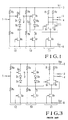
- Fig. 3 shows a conventional single-phase type differential input circuit such as described in Semiconductor Memories, A Handbook of Design Manufacture and Application, second Edition, Betty Prince, Texas Instruments, USA, published by John Wiley & Sons, 1983, with particular reference to figures 5.26 and 9.18 thereof.
- FETs Q1 and Q2 constitute a differential circuit 11 together with load resistor R1 and R2.
- An FET Q3 serves as a constant current source for the differential circuit 11.
- FETs Q4 and Q5 and level shift diodes D1 and D2 constitute a first source follower type bias generating circuit 12.
- a gate bias is applied to the source follower FET Q4 through dividing resistors R3 and R4.
- an output terminal A of the bias generating circuit 12 is connected to the gate electrode of the FET Q1 so that an RF signal supplied to an input terminal 1 is supplied to the differential circuit 11 through the terminal A, thus performing a single-phase operation.
- a second bias generating circuit 13 is constituted by FETs Q6 and Q7 and level shift diodes D3 and D4. A gate bias is applied to the FET Q6 through dividing resistors R5 and R6.
- an output terminal B of the bias generating circuit 13 is connected to the gate electrode of the FET Q2 so that the gate bias serves as a reference voltage.
- Reference symbols V DD and V SS respectively denote power source terminals.
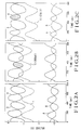
- Figs. 4a to 4c respectively show the results of computer simulation performed by the inventors of the present invention. More specifically, Figs. 4a to 4c respectively show waveforms at the input terminal 1, the input terminals A and B of the differential circuit (reference voltage), and output terminals 3 and 4.
- a differential input circuit comprising a first bias generating circuit for applying an input signal and a bias voltage divided by first dividing resistor means to a first source follower FET and outputting a resultant value through first level shift diode means, a second bias generating circuit for applying a bias voltage divided by second dividing resistor means to a second source follower FET and outputting a resultant value through second level shift diode means, a differential circuit including first and second FETs respectively, said first FET having a gate connected to the output of said first bias generating circuit and said second FET having a gate connected to the output of said second bias generating circuit, a first capacitor for connecting the output of the first FET to a gate electrode of the second FET, and a second capacitor for connecting an output terminal of the second bias generating circuit to a gate electrode of the second source follower FET.
- Fig. 1 shows an embodiment of the present invention. This embodiment is equivalent to the conventional circuit (Fig. 3) except that a capacitor C1 is arranged between the drain electrode (output terminal 3) of a FET Q1 and the gate electrode of an FET Q2, and a capacitor C2 is arranged between the gate electrode of an FET Q6 and a node B. Other components are the same as those of the circuit shown in Fig. 3.
- the capacitor C1 transmits a change in potential of the drain electrode (output terminal 3) of the FET Q1 to the gate electrode of the FET Q2.
- a change in potential of the node (output terminal 3) is opposite in phase to a change in potential applied to the gate of the FET Q1
- the FETs Q1 and Q2 are operated in opposite phases. That is, this operation state is equivalent to a two-phase driving operation.
- a case without the capacitor C2 will be considered first.
- a larger potential change appearing at the gate electrode of the FET Q2 through the capacitor C1 is preferable, because a better two-phase driving operation can be performed with an increase in potential change.
- the potential change is increased with an increase in value of the capacitor C1, because the loss in the capacitor C1 is decreased.
- the value of the capacitor C1 is preferably as large as possible.
- the value of the capacitor C1 is preferably set to be as small as possible. It is apparent from the above description that the value of the capacitor C1 has its upper limit.
- Figs. 5a, 5b,and 5c respectively show the results of computer simulation in which each of load resistors R1 and R2 has a resistance of 750 ⁇ , each of the FETs Q1 and Q2 has a gate width of 20 ⁇ m, a mutual conductance is 300 mS/mm, the differential circuit has a threshold voltage of -0.5 V, and the capacitor C1 has a capacitance of 0.5 pF. It is apparent from waveforms at input terminals A and B of the differential circuit that a two-phase driving operation is performed. It is also apparent that the amplitude of the waveform at the input terminal B is small, and that the waveform at the output terminal 3 exhibits a smaller amplitude than that in Figs. 4a to 4c.
- Figs. 2a, 2b, and 2c respectively show the results of computer simulation which was actually performed while the value of the capacitor C2 was set to be 0.5 pF.
- the potential change at the node B is greatly improved as compared with the case shown in Figs. 5a to 5c.
- an improvement is made in terms of the size of an overlapping portion (a hatched portion in each of Figs. 2b and 2c) of the waveforms at the output terminals 3 and 4 in a case wherein the DC bias value at the input terminal 1 varies by ⁇ 200 mV from the value shown in Fig. 2a.
- the overlapping portion of the waveforms at the output terminals 3 and 4 corresponds to 480 mV in the conventional circuit, as shown in Fig. 4b.
- the overlapping portion corresponds to 440 mV, as shown in Fig. 5b.
- the overlapping portion corresponds to 640 mV, as shown in Fig. 2b. That is, the value of the overlapping portion in the circuit of the embodiment is larger than that in the conventional circuit by 160 mV.
- the circuit of the present invention has high resistance to variations in input DC level so that even if the DC level of the input terminal varies due to any kind of internal or external factor, a large overlapping portion of waveforms can be ensured by preventing the DC levels of two opposite-phase outputs of the differential circuit from being separated from each other too far, thus maintaining the symmetry of the waveforms. With this operation, a normal operation of a differential circuit arranged in the next stage can be maintained.
Landscapes
- Engineering & Computer Science (AREA)
- Power Engineering (AREA)
- Amplifiers (AREA)
- Logic Circuits (AREA)
- Manipulation Of Pulses (AREA)
Claims (4)
- Differenzeingangsschaltung, dadurch gekennzeichnet, daß sie aufweist:
eine erste vorspannungserzeugende Schaltung (12) zum Anlegen eines Eingangssignals und einer Vorspannung, die durch erste Teilerwiderstandsmittel (R₃, R₄) geteilt ist, an einen ersten Source-Folger-FET (Q₄) und zum Ausgeben eines resultierenden Wertes durch erste Pegelverschiebungsdiodenmittel (D₁, D₂);
eine zweite vorspannungserzeugende Schaltung (13) zum Anlegen einer Vorspannung, die durch ein zweites Teilerwiderstandsmittel (R₅, R₆) geteilt ist, an einen zweiten Source-Folger-FET (Q₆) und zum Abgeben eines resultierenden Wertes durch zweite Pegelverschiebungsdiodenmittel (D₃, D₄);
eine Differenzschaltung (11) die erste und zweite FETs (Q₁, Q₂) aufweist, wobei der erste FET (Q₁) mit seinem Gate mit dem Ausgang der ersten vorspannungserzeugenden Schaltung (12) verbunden ist und der zweite FET (Q₂) mit seinem Gate mit dem Ausgang der zweiten vorspannungserzeugenden Schaltung (13) verbunden ist;
einen ersten Kondensator (C₁) zum Verbinden des Ausgangs des ersten FET (Q₁) mit der Gate-Elektrode des zweiten FET (Q₂); und
einen zweiten Kondensator (Q₂) zum Verbinden eines Ausgangsanschlusses der zweiten vorspannungserzeugenden Schaltung (13) mit der Gate-Elektrode des zweiten Source-Folger-FETs (Q₆). - Schaltung nach Anspruch 1, bei der Werte der ersten und zweiten Kondensatoren (C₁, C₂) in Übereinstimmung mit einer Zeitkonstante und einem Verlustwert der Schaltung bei einer dafür verwendeten Frequenz bestimmt sind.
- Schaltung nach Anspruch 1 oder 2, bei der die Differenzschaltung (11) eine Konstantspannungsquelle (Q₃) aufweist, die mit einem Verbindungspunkt zwischen den Drain-Elektroden der ersten und zweiten FETs (Q₁, Q₂) verbunden ist, um dort einen Konstantstrom zuzuführen.
- Schaltung nach einem der Ansprüche 1 bis 3, bei der die Differenzschaltung (11) Lastwiderstände (R₁, R₂) aufweist, die mit den Source-Elektroden der ersten und zweiten FETs (Q₁, Q₂) verbunden sind.
Applications Claiming Priority (2)
| Application Number | Priority Date | Filing Date | Title |
|---|---|---|---|
| JP232122/90 | 1990-08-31 | ||
| JP2232122A JP2634935B2 (ja) | 1990-08-31 | 1990-08-31 | 差動型入力回路 |
Publications (3)
| Publication Number | Publication Date |
|---|---|
| EP0473365A2 EP0473365A2 (de) | 1992-03-04 |
| EP0473365A3 EP0473365A3 (en) | 1992-06-10 |
| EP0473365B1 true EP0473365B1 (de) | 1995-11-02 |
Family
ID=16934353
Family Applications (1)
| Application Number | Title | Priority Date | Filing Date |
|---|---|---|---|
| EP91307741A Expired - Lifetime EP0473365B1 (de) | 1990-08-31 | 1991-08-22 | Differenzeingangsschaltung |
Country Status (4)
| Country | Link |
|---|---|
| US (1) | US5142241A (de) |
| EP (1) | EP0473365B1 (de) |
| JP (1) | JP2634935B2 (de) |
| DE (1) | DE69114227T2 (de) |
Families Citing this family (5)
| Publication number | Priority date | Publication date | Assignee | Title |
|---|---|---|---|---|
| US5394113A (en) * | 1992-08-28 | 1995-02-28 | Harris Corporation | High impedance low-distortion linear amplifier |
| FI107657B (fi) | 1998-03-11 | 2001-09-14 | Nokia Mobile Phones Ltd | Kytkentä differentiaalisen aktiivikomponentin impedanssin säätämiseksi |
| US6424218B1 (en) | 2001-02-28 | 2002-07-23 | International Business Machines Corporation | Programmable differential active voltage divider circuit |
| TWI335128B (en) * | 2006-03-01 | 2010-12-21 | Princeton Technology Corp | Single-end input to differential-ends output low noise amplifier |
| WO2009044441A1 (ja) * | 2007-10-01 | 2009-04-09 | Fujitsu Limited | シングル差動変換装置およびrf受信装置 |
Family Cites Families (1)
| Publication number | Priority date | Publication date | Assignee | Title |
|---|---|---|---|---|
| JP2573666B2 (ja) * | 1988-08-09 | 1997-01-22 | 日本電気株式会社 | 非平衡・平衡変換回路 |
-
1990
- 1990-08-31 JP JP2232122A patent/JP2634935B2/ja not_active Expired - Fee Related
-
1991
- 1991-08-12 US US07/744,087 patent/US5142241A/en not_active Expired - Lifetime
- 1991-08-22 EP EP91307741A patent/EP0473365B1/de not_active Expired - Lifetime
- 1991-08-22 DE DE69114227T patent/DE69114227T2/de not_active Expired - Fee Related
Also Published As
| Publication number | Publication date |
|---|---|
| JPH04117009A (ja) | 1992-04-17 |
| DE69114227T2 (de) | 1996-04-11 |
| US5142241A (en) | 1992-08-25 |
| EP0473365A2 (de) | 1992-03-04 |
| EP0473365A3 (en) | 1992-06-10 |
| DE69114227D1 (de) | 1995-12-07 |
| JP2634935B2 (ja) | 1997-07-30 |
Similar Documents
| Publication | Publication Date | Title |
|---|---|---|
| US4553047A (en) | Regulator for substrate voltage generator | |
| JPS61232708A (ja) | 平衡型差動増幅器 | |
| US4963834A (en) | Operational amplifier | |
| US4340867A (en) | Inverter amplifier | |
| EP0473365B1 (de) | Differenzeingangsschaltung | |
| US4633101A (en) | Semiconductor sample and hold switching circuit | |
| US5751192A (en) | Integrated circuit and method for generating a transimpedance function | |
| US5168180A (en) | Low frequency filter in a monolithic integrated circuit | |
| KR940009398B1 (ko) | 액티브 필터회로 | |
| JPS62261217A (ja) | Mosトランジスタ回路 | |
| US6392454B1 (en) | Shunt regulated push-pull circuit having wide frequency range | |
| US4042843A (en) | Voltage level adaption in MOSFET chips | |
| US4847566A (en) | CMOS Amplifier having enhanced current sinking and capacitance load drive | |
| US6054904A (en) | Voltage controlled ring oscillator and charge pump circuit | |
| JPH051646B2 (de) | ||
| US3603814A (en) | Series-shunt type semiconductor chopper | |
| JPS636908A (ja) | 定電流源回路 | |
| US4591808A (en) | High efficiency oscillator output stage and method of operation | |
| JPH1115541A (ja) | 電源安定化回路および電源安定化回路を備えたpll回路 | |
| JPS6228884B2 (de) | ||
| JP2656683B2 (ja) | 差動型入力回路 | |
| KR20020064775A (ko) | 전기 회로 장치 및 출력 전류 전달 방법 | |
| JPS6396800A (ja) | Cmosサンプルホ−ルド回路 | |
| JPS6349925B2 (de) | ||
| JPS63117503A (ja) | 差動増幅回路 |
Legal Events
| Date | Code | Title | Description |
|---|---|---|---|
| PUAI | Public reference made under article 153(3) epc to a published international application that has entered the european phase |
Free format text: ORIGINAL CODE: 0009012 |
|
| 17P | Request for examination filed |
Effective date: 19910903 |
|
| AK | Designated contracting states |
Kind code of ref document: A2 Designated state(s): DE FR GB |
|
| PUAL | Search report despatched |
Free format text: ORIGINAL CODE: 0009013 |
|
| AK | Designated contracting states |
Kind code of ref document: A3 Designated state(s): DE FR GB |
|
| 17Q | First examination report despatched |
Effective date: 19940712 |
|
| GRAA | (expected) grant |
Free format text: ORIGINAL CODE: 0009210 |
|
| AK | Designated contracting states |
Kind code of ref document: B1 Designated state(s): DE FR GB |
|
| REF | Corresponds to: |
Ref document number: 69114227 Country of ref document: DE Date of ref document: 19951207 |
|
| ET | Fr: translation filed | ||
| PLBE | No opposition filed within time limit |
Free format text: ORIGINAL CODE: 0009261 |
|
| STAA | Information on the status of an ep patent application or granted ep patent |
Free format text: STATUS: NO OPPOSITION FILED WITHIN TIME LIMIT |
|
| 26N | No opposition filed | ||
| REG | Reference to a national code |
Ref country code: GB Ref legal event code: IF02 |
|
| REG | Reference to a national code |
Ref country code: GB Ref legal event code: 732E |
|
| PGFP | Annual fee paid to national office [announced via postgrant information from national office to epo] |
Ref country code: FR Payment date: 20030808 Year of fee payment: 13 |
|
| PGFP | Annual fee paid to national office [announced via postgrant information from national office to epo] |
Ref country code: GB Payment date: 20030820 Year of fee payment: 13 |
|
| PGFP | Annual fee paid to national office [announced via postgrant information from national office to epo] |
Ref country code: DE Payment date: 20030904 Year of fee payment: 13 |
|
| REG | Reference to a national code |
Ref country code: FR Ref legal event code: TP |
|
| PG25 | Lapsed in a contracting state [announced via postgrant information from national office to epo] |
Ref country code: GB Free format text: LAPSE BECAUSE OF NON-PAYMENT OF DUE FEES Effective date: 20040822 |
|
| PG25 | Lapsed in a contracting state [announced via postgrant information from national office to epo] |
Ref country code: DE Free format text: LAPSE BECAUSE OF NON-PAYMENT OF DUE FEES Effective date: 20050301 |
|
| GBPC | Gb: european patent ceased through non-payment of renewal fee |
Effective date: 20040822 |
|
| PG25 | Lapsed in a contracting state [announced via postgrant information from national office to epo] |
Ref country code: FR Free format text: LAPSE BECAUSE OF NON-PAYMENT OF DUE FEES Effective date: 20050429 |
|
| REG | Reference to a national code |
Ref country code: FR Ref legal event code: ST |