EP0472277A1 - Verfahren zur Laser-Trassierung von Substraten - Google Patents
Verfahren zur Laser-Trassierung von Substraten Download PDFInfo
- Publication number
- EP0472277A1 EP0472277A1 EP91306048A EP91306048A EP0472277A1 EP 0472277 A1 EP0472277 A1 EP 0472277A1 EP 91306048 A EP91306048 A EP 91306048A EP 91306048 A EP91306048 A EP 91306048A EP 0472277 A1 EP0472277 A1 EP 0472277A1
- Authority
- EP
- European Patent Office
- Prior art keywords
- substrate
- thick
- resistor
- laser scribing
- film
- Prior art date
- Legal status (The legal status is an assumption and is not a legal conclusion. Google has not performed a legal analysis and makes no representation as to the accuracy of the status listed.)
- Ceased
Links
Images

Classifications
-
- H—ELECTRICITY
- H01—ELECTRIC ELEMENTS
- H01C—RESISTORS
- H01C17/00—Apparatus or processes specially adapted for manufacturing resistors
-
- H—ELECTRICITY
- H05—ELECTRIC TECHNIQUES NOT OTHERWISE PROVIDED FOR
- H05K—PRINTED CIRCUITS; CASINGS OR CONSTRUCTIONAL DETAILS OF ELECTRIC APPARATUS; MANUFACTURE OF ASSEMBLAGES OF ELECTRICAL COMPONENTS
- H05K3/00—Apparatus or processes for manufacturing printed circuits
- H05K3/0011—Working of insulating substrates or insulating layers
- H05K3/0017—Etching of the substrate by chemical or physical means
- H05K3/0026—Etching of the substrate by chemical or physical means by laser ablation
- H05K3/0029—Etching of the substrate by chemical or physical means by laser ablation of inorganic insulating material
-
- H—ELECTRICITY
- H10—SEMICONDUCTOR DEVICES; ELECTRIC SOLID-STATE DEVICES NOT OTHERWISE PROVIDED FOR
- H10D—INORGANIC ELECTRIC SEMICONDUCTOR DEVICES
- H10D84/00—Integrated devices formed in or on semiconductor substrates that comprise only semiconducting layers, e.g. on Si wafers or on GaAs-on-Si wafers
- H10D84/01—Manufacture or treatment
-
- H—ELECTRICITY
- H05—ELECTRIC TECHNIQUES NOT OTHERWISE PROVIDED FOR
- H05K—PRINTED CIRCUITS; CASINGS OR CONSTRUCTIONAL DETAILS OF ELECTRIC APPARATUS; MANUFACTURE OF ASSEMBLAGES OF ELECTRICAL COMPONENTS
- H05K1/00—Printed circuits
- H05K1/02—Details
- H05K1/03—Use of materials for the substrate
- H05K1/0306—Inorganic insulating substrates, e.g. ceramic, glass
-
- H—ELECTRICITY
- H05—ELECTRIC TECHNIQUES NOT OTHERWISE PROVIDED FOR
- H05K—PRINTED CIRCUITS; CASINGS OR CONSTRUCTIONAL DETAILS OF ELECTRIC APPARATUS; MANUFACTURE OF ASSEMBLAGES OF ELECTRICAL COMPONENTS
- H05K1/00—Printed circuits
- H05K1/02—Details
- H05K1/09—Use of materials for the conductive, e.g. metallic pattern
- H05K1/092—Dispersed materials, e.g. conductive pastes or inks
-
- H—ELECTRICITY
- H05—ELECTRIC TECHNIQUES NOT OTHERWISE PROVIDED FOR
- H05K—PRINTED CIRCUITS; CASINGS OR CONSTRUCTIONAL DETAILS OF ELECTRIC APPARATUS; MANUFACTURE OF ASSEMBLAGES OF ELECTRICAL COMPONENTS
- H05K1/00—Printed circuits
- H05K1/16—Printed circuits incorporating printed electric components, e.g. printed resistors, capacitors or inductors
- H05K1/167—Printed circuits incorporating printed electric components, e.g. printed resistors, capacitors or inductors incorporating printed resistors
-
- H—ELECTRICITY
- H05—ELECTRIC TECHNIQUES NOT OTHERWISE PROVIDED FOR
- H05K—PRINTED CIRCUITS; CASINGS OR CONSTRUCTIONAL DETAILS OF ELECTRIC APPARATUS; MANUFACTURE OF ASSEMBLAGES OF ELECTRICAL COMPONENTS
- H05K2203/00—Indexing scheme relating to apparatus or processes for manufacturing printed circuits covered by H05K3/00
- H05K2203/07—Treatments involving liquids, e.g. plating, rinsing
- H05K2203/0756—Uses of liquids, e.g. rinsing, coating, dissolving
- H05K2203/0769—Dissolving insulating materials, e.g. coatings, not used for developing resist after exposure
-
- H—ELECTRICITY
- H05—ELECTRIC TECHNIQUES NOT OTHERWISE PROVIDED FOR
- H05K—PRINTED CIRCUITS; CASINGS OR CONSTRUCTIONAL DETAILS OF ELECTRIC APPARATUS; MANUFACTURE OF ASSEMBLAGES OF ELECTRICAL COMPONENTS
- H05K2203/00—Indexing scheme relating to apparatus or processes for manufacturing printed circuits covered by H05K3/00
- H05K2203/07—Treatments involving liquids, e.g. plating, rinsing
- H05K2203/0779—Treatments involving liquids, e.g. plating, rinsing characterised by the specific liquids involved
- H05K2203/0783—Using solvent, e.g. for cleaning; Regulating solvent content of pastes or coatings for adjusting the viscosity
-
- H—ELECTRICITY
- H05—ELECTRIC TECHNIQUES NOT OTHERWISE PROVIDED FOR
- H05K—PRINTED CIRCUITS; CASINGS OR CONSTRUCTIONAL DETAILS OF ELECTRIC APPARATUS; MANUFACTURE OF ASSEMBLAGES OF ELECTRICAL COMPONENTS
- H05K2203/00—Indexing scheme relating to apparatus or processes for manufacturing printed circuits covered by H05K3/00
- H05K2203/13—Moulding and encapsulation; Deposition techniques; Protective layers
- H05K2203/1377—Protective layers
- H05K2203/1383—Temporary protective insulating layer
-
- H—ELECTRICITY
- H05—ELECTRIC TECHNIQUES NOT OTHERWISE PROVIDED FOR
- H05K—PRINTED CIRCUITS; CASINGS OR CONSTRUCTIONAL DETAILS OF ELECTRIC APPARATUS; MANUFACTURE OF ASSEMBLAGES OF ELECTRICAL COMPONENTS
- H05K3/00—Apparatus or processes for manufacturing printed circuits
- H05K3/0011—Working of insulating substrates or insulating layers
- H05K3/0044—Mechanical working of the substrate, e.g. drilling or punching
- H05K3/0052—Depaneling, i.e. dividing a panel into circuit boards; Working of the edges of circuit boards
-
- H—ELECTRICITY
- H05—ELECTRIC TECHNIQUES NOT OTHERWISE PROVIDED FOR
- H05K—PRINTED CIRCUITS; CASINGS OR CONSTRUCTIONAL DETAILS OF ELECTRIC APPARATUS; MANUFACTURE OF ASSEMBLAGES OF ELECTRICAL COMPONENTS
- H05K3/00—Apparatus or processes for manufacturing printed circuits
- H05K3/0097—Processing two or more printed circuits simultaneously, e.g. made from a common substrate, or temporarily stacked circuit boards
-
- H—ELECTRICITY
- H05—ELECTRIC TECHNIQUES NOT OTHERWISE PROVIDED FOR
- H05K—PRINTED CIRCUITS; CASINGS OR CONSTRUCTIONAL DETAILS OF ELECTRIC APPARATUS; MANUFACTURE OF ASSEMBLAGES OF ELECTRICAL COMPONENTS
- H05K3/00—Apparatus or processes for manufacturing printed circuits
- H05K3/22—Secondary treatment of printed circuits
- H05K3/28—Applying non-metallic protective coatings
Definitions
- This invention relates to a method for laser scribing a substrate and, more particularly, to a method of coating a protective material onto a thick-film resistor element before a laser scribing operation to protect the resistor element during laser scribing.
- a ceramic circuit board It is known in the prior art to make electronic circuit products using a ceramic circuit board.
- One known process for manufacturing a ceramic circuit board is a thick-film process. This process starts with a ceramic plate as the substrate, such as a fired sintered alumina substrate. Conductor paste is first screen printed onto the substrate and fired to form thick-film conductor lines. Thereafter, a pattern of electrical resistance material is screen printed onto the substrate and fired to form thick- film resistor elements which are connected up to the conductor lines. The conductor lines and resistor elements combine to form a plurality of individual thick-film circuits on the substrate.
- each may be laser trimmed to increase the resistance value thereof.
- a laser beam projector is employed which produces a laser beam for evaporating a portion of the resistance material of the resistor element, thereby increasing the resistance value thereof.
- the plurality of thick-film circuits are formed on the substrate, they are separated from one another.
- a laser beam projector which makes scribes in the substrate has been used in the prior art for separating the individual circuits from one another. It has been found, however, that hot-slag ceramic material generated during laser scribing may recondense onto each surface of one or more of the resistor elements. This recondensed material may result in thermal-mechanical damage to a resistor element which may affect the resistance value thereof.
- a method of laser scribing a substrate having a thick-film circuit formed thereon comprises the steps of: coating onto an outer surface of at least one portion of the thick-film circuit a protective material to protect the portion from hot-slag substrate material generated during a laser scribing operation; laser scribing the substrate to separate the thick-film circuit from the remainder of the substrate; and, removing the protective material from the outer surface of the at least one portion of the thick-film circuit.
- the portion of the thick-film circuit may comprise a thick-film resistor, a dielectric layer or a section of a conductor line.
- the substrate may comprise an alumina substrate.
- the protective material coated onto the portion of the thick-film circuit may comprise an organic polymer, such as ethyl cellulose.
- the ethyl cellulose is preferably applied to the portion before the laser scribing step and is removed from the outer surface of the portion by washing the same with a solvent, such as an alcohol.
- the thick-film circuit is formed on a frontside of the substrate and the step of laser scribing the substrate to separate the thick-film circuit from the remainder of the substrate preferably occurs on the frontside of the substrate.
- a method of forming a thick-film circuit having at least one thick-film resistor upon a substrate comprises the steps of: printing the thick-film circuit having the thick-film resistor onto the substrate; laser trimming the thick-film resistor to increase the resistance value thereof; coating onto the outer surface of the resistor a protective material to protect the resistor from hot-slag substrate material generated during a laser scribing operation; laser scribing the substrate to separate the thick-film circuit from the remainder of the substrate; and, removing the protective material from the outer surface of the resistor.
- the step of coating a protective material onto the thick-film resistor occurs subsequent to the laser trimming step.
- the material coated onto the resistor preferably comprises an organic polymer, such as ethyl cellulose.
- the ethyl cellulose is removed from the outer surface of the resistor by washing the outer surface with a solvent, such as an alcohol.
- the step of printing the thick-film circuit having the thick-film resistor onto the substrate comprises the steps of: printing conductor paste onto the substrate to form conductor lines thereon; and, printing resistor paste onto the substrate to form the thick-film resistor thereon.
- the thick-film circuit is printed on a frontside of the substrate and the step of laser scribing the substrate to separate the thick-film circuit from the remainder of the substrate preferably occurs on the frontside of the substrate.
- the substrate may comprise a ceramic material such as alumina.
- an intermediate product for use in the production of thick-film circuits comprises: a substrate; at least two conductor lines formed on the substrate; at least one resistor element formed on the substrate and over a portion of each of the two conductor lines; and a protective material formed over the resistor element to protect the resistor element from hot-slag substrate material generated during a laser scribing operation.
- the protective material may comprise an organic polymer, such as ethyl cellulose.
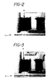
- FIG. 1 there is shown a flow diagram illustrating a method according to the present invention for forming a thick-film circuit 10 having at least one thick-film resistor element 16 upon a substrate 12 and laser scribing the substrate 12 to remove the circuit 10 from the remaining portion of the substrate 12.
- thick-film conductor lines 14 are formed on the substrate 12.
- the thick-film resistor element 16 is then formed on the substrate 12 and over a portion of the conductor lines 14.
- the circuit 10 may include a plurality of conductor lines 14 and one or more resistor elements 16. As can be seen, the substrate 12 is broken away, indicating that multiple thick-film circuits 10 are preferably formed on the substrate 12.
- the substrate 12 is a ceramic substrate such as a fired alumina substrate; although, other substrate materials such as SbN4, AIN, and quartz may be used.
- the conductor lines 14 may be screen printed onto the substrate 12, and subsequently dried and fired.
- the material for the conductor lines 14 may be selected from any one of the alloy families of gold, silver, palladium silvers, platinum gold or palladium golds. After the conductor lines 14 are printed onto the substrate 12, they are typically dried for about 20 minutes at 150°C, and subsequently fired through a belt furnace using a 30-60 minute cycle with 8-10 minutes at a peak temperature of 850°C.
- the resistor element 16 may be formed next, as shown in Fig. 1, using screen printing techniques.
- the material used in forming the resistor element 16 may be a resistor paste such as ruthenium dioxide paste. Other resistor materials containing Pd, carbon, or tantalum nitride may also be used. After the resistor element 16 is screen printed onto the substrate, it is dried and subsequently fired in a similar manner to that of the conductor lines 14.
- the resistor element 16 After the resistor element 16 is formed on the substrate 12, it may be laser trimmed in a known manner, as shown in Fig. 1, in order to increase the resistance value thereof.
- a laser beam projector (not shown) which produces a beam 20 is employed to evaporate a portion of the resistance material of the resistor element 16, thereby increasing the resistance value thereof.
- a protective material 18 is coated onto the resistor element 16 and dried.
- the protective material preferably comprises an organic polymer such as T-type ethyl cellulose which is a 49.6% minimum ethoxyl content cellulose, designated by CAS Abstract # 9004-57-3.
- the ethyl cellulose coating is preferably dried for 5-10 minutes at a temperature of 150°C. The ethyl cellulose coating serves to protect the resistor element 16 from hot- slag substrate material generated during the laser scribing step by acting as a barrier to any substrate material sputtered onto the element 16.
- the substrate 12 is laser scribed by a laser beam projector (not shown) to separate the thick-film circuit 10 from the remaining portion of the substrate 12.
- the substrate is scribed from the topside 24 of the substrate 12.
- the laser projector produces a beam 22 which creates scribes S or score lines in the substrate, each having a depth equal to approximately one-third the thickness of the substrate 12.
- the circuit 10 is then be broken away from the remaining portion of the substrate 12. This may be done manually.
- a plurality of thick-film circuits 10 are formed on the substrate 12 and are separated from one another during the laser scribing operation.
- the resistor element 16 is washed to remove from its outer surface the protective material 18 and any substrate material trapped in the protective material 18. If the protective material is ethyl cellulose, a solvent comprising an alcohol may be used to wash the material 18 from the resistor element 16. A further known solvent which is sold under the tradename PRELETE by Dow Chemical Company may alternatively be used to wash the resistor element 16.
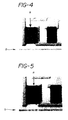
- Each group included 24 thick-film circuits having at least one resistor element formed thereon. Each of the 24 circuits of each group were formed on 24 separate substrates. One resistor element was tested from each circuit in each group to test the resistance shift of the resistor after its respective substrate was laser scribed. Substantially all of the resistance shifts were upward shifts, i.e., the resistance value of the resistor increased.
- the resistor elements were untrimmed and uncoated before laser scribing.
- the resistor elements were untrimmed but were coated with ethyl cellulose before laser scribing.
- the resistor elements were laser trimmed and uncoated before laser scribing.
- the resistor elements were laser trimmed and coated with ethyl cellulose before laser scribing.
- the resistor elements in each group were formed from ruthenium dioxide resistor paste.
- the untrimmed resistors were 40 KOHM value resistors and the trimmed resistors were 60 KOHM value resistors.
- the resistor elements were formed upon a 96% alumina substrate.
- the substrate also included conductor lines thereon formed from silver palladium paste.
- Each resistor was tested for resistance shift after laser scribing and after 24 hours of thermal ageing at 125°C.
- the resistance shifts measured from the untrimmed resistors of groups I and II were averaged for each group and compared to the desired value of 40 KOHM.
- the resistance shifts measured from the trimmed resistors of groups III and IV were averaged for each group and compared to the desired value of 60 KOHM.
- the average shift in resistance for the coated, untrimmed resistors of group II was less than that of the non-coated, untrimmed resistors of group I, both before and after thermal ageing.
- the average shift in resistance for the coated, trimmed resistors of group IV was less than that of the non-coated, trimmed resistors of group III, both before and after thermal ageing.
- a method for protecting a resistor element formed on a substrate during a laser scribing operation.
- the method comprises coating a protective material, preferably ethyl cellulose, onto the resistor element prior to the laser scribing operation to protect the resistor element from hot-slag substrate material generated during the laser scribing operation.
- an ethyl cellulose coating may be used to protect other sensitive areas on a circuit board, such as sensitive sections of conductor lines, dielectric layers and the like. Further, it is contemplated that an ethyl cellulose coating may be employed to protect resistors or the like on multi- layered circuits. It is also contemplated that an ethyl cellulose coating may be employed as an environmental protectant for any circuit element formed or located on a circuit board.
Landscapes
- Engineering & Computer Science (AREA)
- Manufacturing & Machinery (AREA)
- Microelectronics & Electronic Packaging (AREA)
- Chemical & Material Sciences (AREA)
- Inorganic Chemistry (AREA)
- Physics & Mathematics (AREA)
- Optics & Photonics (AREA)
- Apparatuses And Processes For Manufacturing Resistors (AREA)
- Electronic Switches (AREA)
Applications Claiming Priority (2)
| Application Number | Priority Date | Filing Date | Title |
|---|---|---|---|
| US07/570,063 US5116641A (en) | 1990-08-20 | 1990-08-20 | Method for laser scribing substrates |
| US570063 | 1990-08-20 |
Publications (1)
| Publication Number | Publication Date |
|---|---|
| EP0472277A1 true EP0472277A1 (de) | 1992-02-26 |
Family
ID=24278057
Family Applications (1)
| Application Number | Title | Priority Date | Filing Date |
|---|---|---|---|
| EP91306048A Ceased EP0472277A1 (de) | 1990-08-20 | 1991-07-03 | Verfahren zur Laser-Trassierung von Substraten |
Country Status (3)
| Country | Link |
|---|---|
| US (1) | US5116641A (de) |
| EP (1) | EP0472277A1 (de) |
| JP (1) | JPH04233753A (de) |
Cited By (2)
| Publication number | Priority date | Publication date | Assignee | Title |
|---|---|---|---|---|
| GB2320137A (en) * | 1997-05-08 | 1998-06-10 | Yageo Corp | Method for fabrication of a thin film resisitor |
| EP1101228A4 (de) * | 1999-05-11 | 2007-11-07 | Motorola Inc | Polymer dick schichtwiderstand auf ebenem schaltungsplatte |
Families Citing this family (8)
| Publication number | Priority date | Publication date | Assignee | Title |
|---|---|---|---|---|
| DE4345586B4 (de) * | 1992-12-22 | 2009-04-23 | Denso Corp., Kariya-shi | Verfahren zum Erzeugen von Vielfach-Dickschichtsubstraten |
| US5928526A (en) * | 1997-04-29 | 1999-07-27 | Stellex Microwave Systems, Inc. | Method for manufacturing a substrate having an irregular shape |
| US6047463A (en) * | 1998-06-12 | 2000-04-11 | Intermedics Inc. | Embedded trimmable resistors |
| US6631551B1 (en) * | 1998-06-26 | 2003-10-14 | Delphi Technologies, Inc. | Method of forming integral passive electrical components on organic circuit board substrates |
| US6240635B1 (en) * | 1998-11-20 | 2001-06-05 | International Business Machines Corporation | Printed circuit board scrap removal and printed circuit board fabrication process |
| US7204884B2 (en) | 2002-03-22 | 2007-04-17 | Agc Automotive Americas Co. | Laser marking system |
| SG119230A1 (en) * | 2004-07-29 | 2006-02-28 | Micron Technology Inc | Interposer including at least one passive element at least partially defined by a recess formed therein method of manufacture system including same and wafer-scale interposer |
| US8290239B2 (en) * | 2005-10-21 | 2012-10-16 | Orbotech Ltd. | Automatic repair of electric circuits |
Citations (5)
| Publication number | Priority date | Publication date | Assignee | Title |
|---|---|---|---|---|
| US4486738A (en) * | 1982-02-16 | 1984-12-04 | General Electric Ceramics, Inc. | High reliability electrical components |
| EP0167198A1 (de) * | 1984-06-22 | 1986-01-08 | Laboratoires D'electronique Et De Physique Appliquee L.E.P. | Ausgangsmischung für eine isolierende Bleiglas enthaltende Zusammensetzung, eine solche Mischung enthaltende Siebdrucktinte und Verwendung dieser Tinte zum Schützen von hybriden Mikroschaltungen auf keramischem Substrat |
| US4694568A (en) * | 1982-01-07 | 1987-09-22 | North American Philips Corporation | Method of manufacturing chip resistors with edge around terminations |
| US4788523A (en) * | 1987-12-10 | 1988-11-29 | United States Of America | Viad chip resistor |
| EP0337412A2 (de) * | 1988-04-15 | 1989-10-18 | E.I. Du Pont De Nemours And Company | Abdichtungszusammensetzung |
Family Cites Families (11)
| Publication number | Priority date | Publication date | Assignee | Title |
|---|---|---|---|---|
| US3066033A (en) * | 1960-07-29 | 1962-11-27 | American Cyanamid Co | Cellulose ester coating composition |
| US4082830A (en) * | 1972-05-10 | 1978-04-04 | W. R. Grace & Co. | Process of forming a protective coating and shipping the coating from the surface being protected when no longer required |
| US4071639A (en) * | 1975-10-22 | 1978-01-31 | Combustion Engineering, Inc. | Coating material and method |
| US4081653A (en) * | 1976-12-27 | 1978-03-28 | Western Electric Co., Inc. | Removal of thin films from substrates by laser induced explosion |
| US4301194A (en) * | 1979-05-04 | 1981-11-17 | Purex Corporation | Chemical milling maskant application process |
| US4288530A (en) * | 1979-10-15 | 1981-09-08 | Motorola, Inc. | Method of tuning apparatus by low power laser beam removal |
| US4352835A (en) * | 1981-07-01 | 1982-10-05 | Western Electric Co., Inc. | Masking portions of a substrate |
| US4783421A (en) * | 1985-04-15 | 1988-11-08 | Solarex Corporation | Method for manufacturing electrical contacts for a thin-film semiconductor device |
| JPS6240787A (ja) * | 1985-08-16 | 1987-02-21 | New Japan Radio Co Ltd | 厚膜チツプ抵抗 |
| US4931323A (en) * | 1987-12-10 | 1990-06-05 | Texas Instruments Incorporated | Thick film copper conductor patterning by laser |
| JPH02250390A (ja) * | 1989-03-24 | 1990-10-08 | Ngk Insulators Ltd | 給電用セラミック基板の製造法 |
-
1990
- 1990-08-20 US US07/570,063 patent/US5116641A/en not_active Expired - Fee Related
-
1991
- 1991-07-03 EP EP91306048A patent/EP0472277A1/de not_active Ceased
- 1991-08-08 JP JP3199346A patent/JPH04233753A/ja active Pending
Patent Citations (5)
| Publication number | Priority date | Publication date | Assignee | Title |
|---|---|---|---|---|
| US4694568A (en) * | 1982-01-07 | 1987-09-22 | North American Philips Corporation | Method of manufacturing chip resistors with edge around terminations |
| US4486738A (en) * | 1982-02-16 | 1984-12-04 | General Electric Ceramics, Inc. | High reliability electrical components |
| EP0167198A1 (de) * | 1984-06-22 | 1986-01-08 | Laboratoires D'electronique Et De Physique Appliquee L.E.P. | Ausgangsmischung für eine isolierende Bleiglas enthaltende Zusammensetzung, eine solche Mischung enthaltende Siebdrucktinte und Verwendung dieser Tinte zum Schützen von hybriden Mikroschaltungen auf keramischem Substrat |
| US4788523A (en) * | 1987-12-10 | 1988-11-29 | United States Of America | Viad chip resistor |
| EP0337412A2 (de) * | 1988-04-15 | 1989-10-18 | E.I. Du Pont De Nemours And Company | Abdichtungszusammensetzung |
Non-Patent Citations (2)
| Title |
|---|
| PATENT ABSTRACTS OF JAPAN vol. 11, no. 224 (E-525)(2671) 21 July 1987, & JP-A-62 040787 (NEW JAPAN RADIO CO.LTD.) 21 February 1987, * |
| PATENT ABSTRACTS OF JAPAN vol. 14, no. 576 (E-1016) 21 December 1990, & JP-A-02 250390 (NGK INSULATORS LTD.) 08 October 1990, * |
Cited By (3)
| Publication number | Priority date | Publication date | Assignee | Title |
|---|---|---|---|---|
| GB2320137A (en) * | 1997-05-08 | 1998-06-10 | Yageo Corp | Method for fabrication of a thin film resisitor |
| GB2320137B (en) * | 1997-05-08 | 1998-11-18 | Yageo Corp | Method for fabrication of thin film resistor |
| EP1101228A4 (de) * | 1999-05-11 | 2007-11-07 | Motorola Inc | Polymer dick schichtwiderstand auf ebenem schaltungsplatte |
Also Published As
| Publication number | Publication date |
|---|---|
| US5116641A (en) | 1992-05-26 |
| JPH04233753A (ja) | 1992-08-21 |
Similar Documents
| Publication | Publication Date | Title |
|---|---|---|
| US5116641A (en) | Method for laser scribing substrates | |
| US6233817B1 (en) | Method of forming thick-film hybrid circuit on a metal circuit board | |
| US4031272A (en) | Hybrid integrated circuit including thick film resistors and thin film conductors and technique for fabrication thereof | |
| US6120835A (en) | Process for manufacture of thick film hydrogen sensors | |
| US5206624A (en) | Intermediate product for use in the production of thick-film circuits | |
| US5593722A (en) | Method of producing thick multi-layer substrates | |
| US6521355B1 (en) | Optical color tracer indentifier in metal paste that bleed to greensheet | |
| JP2526347B2 (ja) | 封入剤組成物 | |
| WO2020134016A1 (zh) | 一种高精度高可靠Ti/W-Cu-Au复合电极热敏芯片 | |
| JP3129170B2 (ja) | 角形薄膜チップ抵抗器の製造方法 | |
| US4694568A (en) | Method of manufacturing chip resistors with edge around terminations | |
| US5723073A (en) | Conductive paste containing 2-tetradecanol and ceramic circuit substrate using the same | |
| EP0054101B1 (de) | Verfahren und Vorrichtung zur Überwachung des Lösungsmittelgehalts von keramischen grünen Plättchen | |
| JPH04154104A (ja) | 積層セラミックコンデンサ | |
| JP3304130B2 (ja) | 角形薄膜チップ抵抗器の製造方法 | |
| JP3635669B2 (ja) | 厚膜多層基板の製造方法 | |
| JP2971605B2 (ja) | 積層体 | |
| JP3136682B2 (ja) | 多層配線基板の製造方法 | |
| WO1997033311A1 (en) | Method for making electrical connections | |
| GB2393332A (en) | Method of fabricating a ceramic circuit board using conductor paste with chosen shrinkage properties. | |
| JPH01300592A (ja) | 厚膜多層配線基板 | |
| JP3719518B2 (ja) | 厚膜多層基板の製造方法 | |
| JP2927004B2 (ja) | 集積回路におけるトリミング方法 | |
| JPH0575262A (ja) | セラミツク多層配線基板の製造方法 | |
| Ferraris | Thin film resistors for high precision networks |
Legal Events
| Date | Code | Title | Description |
|---|---|---|---|
| PUAI | Public reference made under article 153(3) epc to a published international application that has entered the european phase |
Free format text: ORIGINAL CODE: 0009012 |
|
| AK | Designated contracting states |
Kind code of ref document: A1 Designated state(s): DE FR GB NL |
|
| 17P | Request for examination filed |
Effective date: 19920730 |
|
| 17Q | First examination report despatched |
Effective date: 19941215 |
|
| GRAG | Despatch of communication of intention to grant |
Free format text: ORIGINAL CODE: EPIDOS AGRA |
|
| STAA | Information on the status of an ep patent application or granted ep patent |
Free format text: STATUS: THE APPLICATION HAS BEEN REFUSED |
|
| 18R | Application refused |
Effective date: 19960706 |