EP0472277A1 - Method for laser scribing substrates - Google Patents
Method for laser scribing substrates Download PDFInfo
- Publication number
- EP0472277A1 EP0472277A1 EP91306048A EP91306048A EP0472277A1 EP 0472277 A1 EP0472277 A1 EP 0472277A1 EP 91306048 A EP91306048 A EP 91306048A EP 91306048 A EP91306048 A EP 91306048A EP 0472277 A1 EP0472277 A1 EP 0472277A1
- Authority
- EP
- European Patent Office
- Prior art keywords
- substrate
- thick
- resistor
- laser scribing
- film
- Prior art date
- Legal status (The legal status is an assumption and is not a legal conclusion. Google has not performed a legal analysis and makes no representation as to the accuracy of the status listed.)
- Ceased
Links
- 239000000758 substrate Substances 0.000 title claims abstract description 113
- 238000000034 method Methods 0.000 title claims abstract description 25
- 239000000463 material Substances 0.000 claims abstract description 44
- 239000004020 conductor Substances 0.000 claims abstract description 23
- 230000001681 protective effect Effects 0.000 claims abstract description 23
- ZZSNKZQZMQGXPY-UHFFFAOYSA-N Ethyl cellulose Chemical compound CCOCC1OC(OC)C(OCC)C(OCC)C1OC1C(O)C(O)C(OC)C(CO)O1 ZZSNKZQZMQGXPY-UHFFFAOYSA-N 0.000 claims abstract description 22
- 239000001856 Ethyl cellulose Substances 0.000 claims abstract description 21
- 229920001249 ethyl cellulose Polymers 0.000 claims abstract description 21
- 235000019325 ethyl cellulose Nutrition 0.000 claims abstract description 21
- 239000002893 slag Substances 0.000 claims abstract description 14
- 239000002904 solvent Substances 0.000 claims abstract description 6
- 238000009966 trimming Methods 0.000 claims abstract description 6
- 238000005406 washing Methods 0.000 claims abstract description 4
- 239000011248 coating agent Substances 0.000 claims description 14
- 238000000576 coating method Methods 0.000 claims description 14
- 238000007639 printing Methods 0.000 claims description 8
- 239000000919 ceramic Substances 0.000 claims description 6
- 238000004519 manufacturing process Methods 0.000 claims description 3
- 239000013067 intermediate product Substances 0.000 claims description 2
- 229910010293 ceramic material Inorganic materials 0.000 abstract description 5
- 230000032683 aging Effects 0.000 description 9
- KDLHZDBZIXYQEI-UHFFFAOYSA-N Palladium Chemical compound [Pd] KDLHZDBZIXYQEI-UHFFFAOYSA-N 0.000 description 5
- PNEYBMLMFCGWSK-UHFFFAOYSA-N aluminium oxide Inorganic materials [O-2].[O-2].[O-2].[Al+3].[Al+3] PNEYBMLMFCGWSK-UHFFFAOYSA-N 0.000 description 5
- 239000011521 glass Substances 0.000 description 5
- 229920000620 organic polymer Polymers 0.000 description 4
- WOCIAKWEIIZHES-UHFFFAOYSA-N ruthenium(iv) oxide Chemical compound O=[Ru]=O WOCIAKWEIIZHES-UHFFFAOYSA-N 0.000 description 4
- LFQSCWFLJHTTHZ-UHFFFAOYSA-N Ethanol Chemical compound CCO LFQSCWFLJHTTHZ-UHFFFAOYSA-N 0.000 description 3
- 238000010586 diagram Methods 0.000 description 2
- 229910052763 palladium Inorganic materials 0.000 description 2
- OKTJSMMVPCPJKN-UHFFFAOYSA-N Carbon Chemical compound [C] OKTJSMMVPCPJKN-UHFFFAOYSA-N 0.000 description 1
- BQCADISMDOOEFD-UHFFFAOYSA-N Silver Chemical compound [Ag] BQCADISMDOOEFD-UHFFFAOYSA-N 0.000 description 1
- 230000002411 adverse Effects 0.000 description 1
- 239000000956 alloy Substances 0.000 description 1
- 229910045601 alloy Inorganic materials 0.000 description 1
- 230000004888 barrier function Effects 0.000 description 1
- 229910052799 carbon Inorganic materials 0.000 description 1
- 229920002678 cellulose Polymers 0.000 description 1
- 239000001913 cellulose Substances 0.000 description 1
- 230000007613 environmental effect Effects 0.000 description 1
- -1 ethoxyl Chemical group 0.000 description 1
- 238000001704 evaporation Methods 0.000 description 1
- 238000010304 firing Methods 0.000 description 1
- PCHJSUWPFVWCPO-UHFFFAOYSA-N gold Chemical compound [Au] PCHJSUWPFVWCPO-UHFFFAOYSA-N 0.000 description 1
- 229910052737 gold Inorganic materials 0.000 description 1
- 239000010931 gold Substances 0.000 description 1
- JUWSSMXCCAMYGX-UHFFFAOYSA-N gold platinum Chemical compound [Pt].[Au] JUWSSMXCCAMYGX-UHFFFAOYSA-N 0.000 description 1
- 230000017525 heat dissipation Effects 0.000 description 1
- 238000012986 modification Methods 0.000 description 1
- 230000004048 modification Effects 0.000 description 1
- SWELZOZIOHGSPA-UHFFFAOYSA-N palladium silver Chemical compound [Pd].[Ag] SWELZOZIOHGSPA-UHFFFAOYSA-N 0.000 description 1
- 239000002245 particle Substances 0.000 description 1
- 239000000047 product Substances 0.000 description 1
- 239000011253 protective coating Substances 0.000 description 1
- 239000010453 quartz Substances 0.000 description 1
- 238000007650 screen-printing Methods 0.000 description 1
- VYPSYNLAJGMNEJ-UHFFFAOYSA-N silicon dioxide Inorganic materials O=[Si]=O VYPSYNLAJGMNEJ-UHFFFAOYSA-N 0.000 description 1
- 229910052709 silver Inorganic materials 0.000 description 1
- 239000004332 silver Substances 0.000 description 1
- 239000000126 substance Substances 0.000 description 1
- MZLGASXMSKOWSE-UHFFFAOYSA-N tantalum nitride Chemical compound [Ta]#N MZLGASXMSKOWSE-UHFFFAOYSA-N 0.000 description 1
- 230000000007 visual effect Effects 0.000 description 1
- 238000011179 visual inspection Methods 0.000 description 1
Images

Classifications
-
- H—ELECTRICITY
- H01—ELECTRIC ELEMENTS
- H01C—RESISTORS
- H01C17/00—Apparatus or processes specially adapted for manufacturing resistors
-
- H—ELECTRICITY
- H01—ELECTRIC ELEMENTS
- H01L—SEMICONDUCTOR DEVICES NOT COVERED BY CLASS H10
- H01L21/00—Processes or apparatus adapted for the manufacture or treatment of semiconductor or solid state devices or of parts thereof
- H01L21/70—Manufacture or treatment of devices consisting of a plurality of solid state components formed in or on a common substrate or of parts thereof; Manufacture of integrated circuit devices or of parts thereof
- H01L21/702—Manufacture or treatment of devices consisting of a plurality of solid state components formed in or on a common substrate or of parts thereof; Manufacture of integrated circuit devices or of parts thereof of thick-or thin-film circuits or parts thereof
- H01L21/705—Manufacture or treatment of devices consisting of a plurality of solid state components formed in or on a common substrate or of parts thereof; Manufacture of integrated circuit devices or of parts thereof of thick-or thin-film circuits or parts thereof of thick-film circuits or parts thereof
-
- H—ELECTRICITY
- H05—ELECTRIC TECHNIQUES NOT OTHERWISE PROVIDED FOR
- H05K—PRINTED CIRCUITS; CASINGS OR CONSTRUCTIONAL DETAILS OF ELECTRIC APPARATUS; MANUFACTURE OF ASSEMBLAGES OF ELECTRICAL COMPONENTS
- H05K3/00—Apparatus or processes for manufacturing printed circuits
- H05K3/0011—Working of insulating substrates or insulating layers
- H05K3/0017—Etching of the substrate by chemical or physical means
- H05K3/0026—Etching of the substrate by chemical or physical means by laser ablation
- H05K3/0029—Etching of the substrate by chemical or physical means by laser ablation of inorganic insulating material
-
- H—ELECTRICITY
- H05—ELECTRIC TECHNIQUES NOT OTHERWISE PROVIDED FOR
- H05K—PRINTED CIRCUITS; CASINGS OR CONSTRUCTIONAL DETAILS OF ELECTRIC APPARATUS; MANUFACTURE OF ASSEMBLAGES OF ELECTRICAL COMPONENTS
- H05K1/00—Printed circuits
- H05K1/02—Details
- H05K1/03—Use of materials for the substrate
- H05K1/0306—Inorganic insulating substrates, e.g. ceramic, glass
-
- H—ELECTRICITY
- H05—ELECTRIC TECHNIQUES NOT OTHERWISE PROVIDED FOR
- H05K—PRINTED CIRCUITS; CASINGS OR CONSTRUCTIONAL DETAILS OF ELECTRIC APPARATUS; MANUFACTURE OF ASSEMBLAGES OF ELECTRICAL COMPONENTS
- H05K1/00—Printed circuits
- H05K1/02—Details
- H05K1/09—Use of materials for the conductive, e.g. metallic pattern
- H05K1/092—Dispersed materials, e.g. conductive pastes or inks
-
- H—ELECTRICITY
- H05—ELECTRIC TECHNIQUES NOT OTHERWISE PROVIDED FOR
- H05K—PRINTED CIRCUITS; CASINGS OR CONSTRUCTIONAL DETAILS OF ELECTRIC APPARATUS; MANUFACTURE OF ASSEMBLAGES OF ELECTRICAL COMPONENTS
- H05K1/00—Printed circuits
- H05K1/16—Printed circuits incorporating printed electric components, e.g. printed resistor, capacitor, inductor
- H05K1/167—Printed circuits incorporating printed electric components, e.g. printed resistor, capacitor, inductor incorporating printed resistors
-
- H—ELECTRICITY
- H05—ELECTRIC TECHNIQUES NOT OTHERWISE PROVIDED FOR
- H05K—PRINTED CIRCUITS; CASINGS OR CONSTRUCTIONAL DETAILS OF ELECTRIC APPARATUS; MANUFACTURE OF ASSEMBLAGES OF ELECTRICAL COMPONENTS
- H05K2203/00—Indexing scheme relating to apparatus or processes for manufacturing printed circuits covered by H05K3/00
- H05K2203/07—Treatments involving liquids, e.g. plating, rinsing
- H05K2203/0756—Uses of liquids, e.g. rinsing, coating, dissolving
- H05K2203/0769—Dissolving insulating materials, e.g. coatings, not used for developing resist after exposure
-
- H—ELECTRICITY
- H05—ELECTRIC TECHNIQUES NOT OTHERWISE PROVIDED FOR
- H05K—PRINTED CIRCUITS; CASINGS OR CONSTRUCTIONAL DETAILS OF ELECTRIC APPARATUS; MANUFACTURE OF ASSEMBLAGES OF ELECTRICAL COMPONENTS
- H05K2203/00—Indexing scheme relating to apparatus or processes for manufacturing printed circuits covered by H05K3/00
- H05K2203/07—Treatments involving liquids, e.g. plating, rinsing
- H05K2203/0779—Treatments involving liquids, e.g. plating, rinsing characterised by the specific liquids involved
- H05K2203/0783—Using solvent, e.g. for cleaning; Regulating solvent content of pastes or coatings for adjusting the viscosity
-
- H—ELECTRICITY
- H05—ELECTRIC TECHNIQUES NOT OTHERWISE PROVIDED FOR
- H05K—PRINTED CIRCUITS; CASINGS OR CONSTRUCTIONAL DETAILS OF ELECTRIC APPARATUS; MANUFACTURE OF ASSEMBLAGES OF ELECTRICAL COMPONENTS
- H05K2203/00—Indexing scheme relating to apparatus or processes for manufacturing printed circuits covered by H05K3/00
- H05K2203/13—Moulding and encapsulation; Deposition techniques; Protective layers
- H05K2203/1377—Protective layers
- H05K2203/1383—Temporary protective insulating layer
-
- H—ELECTRICITY
- H05—ELECTRIC TECHNIQUES NOT OTHERWISE PROVIDED FOR
- H05K—PRINTED CIRCUITS; CASINGS OR CONSTRUCTIONAL DETAILS OF ELECTRIC APPARATUS; MANUFACTURE OF ASSEMBLAGES OF ELECTRICAL COMPONENTS
- H05K3/00—Apparatus or processes for manufacturing printed circuits
- H05K3/0011—Working of insulating substrates or insulating layers
- H05K3/0044—Mechanical working of the substrate, e.g. drilling or punching
- H05K3/0052—Depaneling, i.e. dividing a panel into circuit boards; Working of the edges of circuit boards
-
- H—ELECTRICITY
- H05—ELECTRIC TECHNIQUES NOT OTHERWISE PROVIDED FOR
- H05K—PRINTED CIRCUITS; CASINGS OR CONSTRUCTIONAL DETAILS OF ELECTRIC APPARATUS; MANUFACTURE OF ASSEMBLAGES OF ELECTRICAL COMPONENTS
- H05K3/00—Apparatus or processes for manufacturing printed circuits
- H05K3/0097—Processing two or more printed circuits simultaneously, e.g. made from a common substrate, or temporarily stacked circuit boards
-
- H—ELECTRICITY
- H05—ELECTRIC TECHNIQUES NOT OTHERWISE PROVIDED FOR
- H05K—PRINTED CIRCUITS; CASINGS OR CONSTRUCTIONAL DETAILS OF ELECTRIC APPARATUS; MANUFACTURE OF ASSEMBLAGES OF ELECTRICAL COMPONENTS
- H05K3/00—Apparatus or processes for manufacturing printed circuits
- H05K3/22—Secondary treatment of printed circuits
- H05K3/28—Applying non-metallic protective coatings
Definitions
- This invention relates to a method for laser scribing a substrate and, more particularly, to a method of coating a protective material onto a thick-film resistor element before a laser scribing operation to protect the resistor element during laser scribing.
- a ceramic circuit board It is known in the prior art to make electronic circuit products using a ceramic circuit board.
- One known process for manufacturing a ceramic circuit board is a thick-film process. This process starts with a ceramic plate as the substrate, such as a fired sintered alumina substrate. Conductor paste is first screen printed onto the substrate and fired to form thick-film conductor lines. Thereafter, a pattern of electrical resistance material is screen printed onto the substrate and fired to form thick- film resistor elements which are connected up to the conductor lines. The conductor lines and resistor elements combine to form a plurality of individual thick-film circuits on the substrate.
- each may be laser trimmed to increase the resistance value thereof.
- a laser beam projector is employed which produces a laser beam for evaporating a portion of the resistance material of the resistor element, thereby increasing the resistance value thereof.
- the plurality of thick-film circuits are formed on the substrate, they are separated from one another.
- a laser beam projector which makes scribes in the substrate has been used in the prior art for separating the individual circuits from one another. It has been found, however, that hot-slag ceramic material generated during laser scribing may recondense onto each surface of one or more of the resistor elements. This recondensed material may result in thermal-mechanical damage to a resistor element which may affect the resistance value thereof.
- a method of laser scribing a substrate having a thick-film circuit formed thereon comprises the steps of: coating onto an outer surface of at least one portion of the thick-film circuit a protective material to protect the portion from hot-slag substrate material generated during a laser scribing operation; laser scribing the substrate to separate the thick-film circuit from the remainder of the substrate; and, removing the protective material from the outer surface of the at least one portion of the thick-film circuit.
- the portion of the thick-film circuit may comprise a thick-film resistor, a dielectric layer or a section of a conductor line.
- the substrate may comprise an alumina substrate.
- the protective material coated onto the portion of the thick-film circuit may comprise an organic polymer, such as ethyl cellulose.
- the ethyl cellulose is preferably applied to the portion before the laser scribing step and is removed from the outer surface of the portion by washing the same with a solvent, such as an alcohol.
- the thick-film circuit is formed on a frontside of the substrate and the step of laser scribing the substrate to separate the thick-film circuit from the remainder of the substrate preferably occurs on the frontside of the substrate.
- a method of forming a thick-film circuit having at least one thick-film resistor upon a substrate comprises the steps of: printing the thick-film circuit having the thick-film resistor onto the substrate; laser trimming the thick-film resistor to increase the resistance value thereof; coating onto the outer surface of the resistor a protective material to protect the resistor from hot-slag substrate material generated during a laser scribing operation; laser scribing the substrate to separate the thick-film circuit from the remainder of the substrate; and, removing the protective material from the outer surface of the resistor.
- the step of coating a protective material onto the thick-film resistor occurs subsequent to the laser trimming step.
- the material coated onto the resistor preferably comprises an organic polymer, such as ethyl cellulose.
- the ethyl cellulose is removed from the outer surface of the resistor by washing the outer surface with a solvent, such as an alcohol.
- the step of printing the thick-film circuit having the thick-film resistor onto the substrate comprises the steps of: printing conductor paste onto the substrate to form conductor lines thereon; and, printing resistor paste onto the substrate to form the thick-film resistor thereon.
- the thick-film circuit is printed on a frontside of the substrate and the step of laser scribing the substrate to separate the thick-film circuit from the remainder of the substrate preferably occurs on the frontside of the substrate.
- the substrate may comprise a ceramic material such as alumina.
- an intermediate product for use in the production of thick-film circuits comprises: a substrate; at least two conductor lines formed on the substrate; at least one resistor element formed on the substrate and over a portion of each of the two conductor lines; and a protective material formed over the resistor element to protect the resistor element from hot-slag substrate material generated during a laser scribing operation.
- the protective material may comprise an organic polymer, such as ethyl cellulose.
- FIG. 1 there is shown a flow diagram illustrating a method according to the present invention for forming a thick-film circuit 10 having at least one thick-film resistor element 16 upon a substrate 12 and laser scribing the substrate 12 to remove the circuit 10 from the remaining portion of the substrate 12.
- thick-film conductor lines 14 are formed on the substrate 12.
- the thick-film resistor element 16 is then formed on the substrate 12 and over a portion of the conductor lines 14.
- the circuit 10 may include a plurality of conductor lines 14 and one or more resistor elements 16. As can be seen, the substrate 12 is broken away, indicating that multiple thick-film circuits 10 are preferably formed on the substrate 12.
- the substrate 12 is a ceramic substrate such as a fired alumina substrate; although, other substrate materials such as SbN4, AIN, and quartz may be used.
- the conductor lines 14 may be screen printed onto the substrate 12, and subsequently dried and fired.
- the material for the conductor lines 14 may be selected from any one of the alloy families of gold, silver, palladium silvers, platinum gold or palladium golds. After the conductor lines 14 are printed onto the substrate 12, they are typically dried for about 20 minutes at 150°C, and subsequently fired through a belt furnace using a 30-60 minute cycle with 8-10 minutes at a peak temperature of 850°C.
- the resistor element 16 may be formed next, as shown in Fig. 1, using screen printing techniques.
- the material used in forming the resistor element 16 may be a resistor paste such as ruthenium dioxide paste. Other resistor materials containing Pd, carbon, or tantalum nitride may also be used. After the resistor element 16 is screen printed onto the substrate, it is dried and subsequently fired in a similar manner to that of the conductor lines 14.
- the resistor element 16 After the resistor element 16 is formed on the substrate 12, it may be laser trimmed in a known manner, as shown in Fig. 1, in order to increase the resistance value thereof.
- a laser beam projector (not shown) which produces a beam 20 is employed to evaporate a portion of the resistance material of the resistor element 16, thereby increasing the resistance value thereof.
- a protective material 18 is coated onto the resistor element 16 and dried.
- the protective material preferably comprises an organic polymer such as T-type ethyl cellulose which is a 49.6% minimum ethoxyl content cellulose, designated by CAS Abstract # 9004-57-3.
- the ethyl cellulose coating is preferably dried for 5-10 minutes at a temperature of 150°C. The ethyl cellulose coating serves to protect the resistor element 16 from hot- slag substrate material generated during the laser scribing step by acting as a barrier to any substrate material sputtered onto the element 16.
- the substrate 12 is laser scribed by a laser beam projector (not shown) to separate the thick-film circuit 10 from the remaining portion of the substrate 12.
- the substrate is scribed from the topside 24 of the substrate 12.
- the laser projector produces a beam 22 which creates scribes S or score lines in the substrate, each having a depth equal to approximately one-third the thickness of the substrate 12.
- the circuit 10 is then be broken away from the remaining portion of the substrate 12. This may be done manually.
- a plurality of thick-film circuits 10 are formed on the substrate 12 and are separated from one another during the laser scribing operation.
- the resistor element 16 is washed to remove from its outer surface the protective material 18 and any substrate material trapped in the protective material 18. If the protective material is ethyl cellulose, a solvent comprising an alcohol may be used to wash the material 18 from the resistor element 16. A further known solvent which is sold under the tradename PRELETE by Dow Chemical Company may alternatively be used to wash the resistor element 16.
- Each group included 24 thick-film circuits having at least one resistor element formed thereon. Each of the 24 circuits of each group were formed on 24 separate substrates. One resistor element was tested from each circuit in each group to test the resistance shift of the resistor after its respective substrate was laser scribed. Substantially all of the resistance shifts were upward shifts, i.e., the resistance value of the resistor increased.
- the resistor elements were untrimmed and uncoated before laser scribing.
- the resistor elements were untrimmed but were coated with ethyl cellulose before laser scribing.
- the resistor elements were laser trimmed and uncoated before laser scribing.
- the resistor elements were laser trimmed and coated with ethyl cellulose before laser scribing.
- the resistor elements in each group were formed from ruthenium dioxide resistor paste.
- the untrimmed resistors were 40 KOHM value resistors and the trimmed resistors were 60 KOHM value resistors.
- the resistor elements were formed upon a 96% alumina substrate.
- the substrate also included conductor lines thereon formed from silver palladium paste.
- Each resistor was tested for resistance shift after laser scribing and after 24 hours of thermal ageing at 125°C.
- the resistance shifts measured from the untrimmed resistors of groups I and II were averaged for each group and compared to the desired value of 40 KOHM.
- the resistance shifts measured from the trimmed resistors of groups III and IV were averaged for each group and compared to the desired value of 60 KOHM.
- the average shift in resistance for the coated, untrimmed resistors of group II was less than that of the non-coated, untrimmed resistors of group I, both before and after thermal ageing.
- the average shift in resistance for the coated, trimmed resistors of group IV was less than that of the non-coated, trimmed resistors of group III, both before and after thermal ageing.
- a method for protecting a resistor element formed on a substrate during a laser scribing operation.
- the method comprises coating a protective material, preferably ethyl cellulose, onto the resistor element prior to the laser scribing operation to protect the resistor element from hot-slag substrate material generated during the laser scribing operation.
- an ethyl cellulose coating may be used to protect other sensitive areas on a circuit board, such as sensitive sections of conductor lines, dielectric layers and the like. Further, it is contemplated that an ethyl cellulose coating may be employed to protect resistors or the like on multi- layered circuits. It is also contemplated that an ethyl cellulose coating may be employed as an environmental protectant for any circuit element formed or located on a circuit board.
Abstract
A method is provided for forming a thick-film circuit (10) having at least one thick-film resistor element (16) upon a substrate and laser scribing the substrate (12) to remove the circuit from the remaining portion of the substrate. A thick-film circuit (10) comprising conductor lines (14) and at least one resistor element (16) is first printed upon the substrate (12). Thereafter, the resistor element (16) may be laser trimmed to increase the resistance value thereof. After laser trimming, a protective material (18) such as ethyl cellulose is coated onto the outer surface of the resistor element to protect it from hot-slag ceramic material generated during a laser scribing operation. The substrate (12) is then topside laser scribed to separate the thick-film circuit from the remaining portion of the substrate. Following laser scribing, the protective material (18) is removed by washing the resistor element with a solvent.
Description
- This invention relates to a method for laser scribing a substrate and, more particularly, to a method of coating a protective material onto a thick-film resistor element before a laser scribing operation to protect the resistor element during laser scribing.
- It is known in the prior art to make electronic circuit products using a ceramic circuit board. One known process for manufacturing a ceramic circuit board is a thick-film process. This process starts with a ceramic plate as the substrate, such as a fired sintered alumina substrate. Conductor paste is first screen printed onto the substrate and fired to form thick-film conductor lines. Thereafter, a pattern of electrical resistance material is screen printed onto the substrate and fired to form thick- film resistor elements which are connected up to the conductor lines. The conductor lines and resistor elements combine to form a plurality of individual thick-film circuits on the substrate.
- After the thick-film resistor elements are formed on the substrate, each may be laser trimmed to increase the resistance value thereof. A laser beam projector is employed which produces a laser beam for evaporating a portion of the resistance material of the resistor element, thereby increasing the resistance value thereof.
- After the plurality of thick-film circuits are formed on the substrate, they are separated from one another. A laser beam projector which makes scribes in the substrate has been used in the prior art for separating the individual circuits from one another. It has been found, however, that hot-slag ceramic material generated during laser scribing may recondense onto each surface of one or more of the resistor elements. This recondensed material may result in thermal-mechanical damage to a resistor element which may affect the resistance value thereof.
- Attempts have been made in the past to avoid damage to resistor elements during a laser scribing operation. For example, laser scribing from the backside of the substrate away from the thick-film circuits has been attempted in the prior art. Such a method, however, has not been found to be acceptable. This is because mechanical damage to the resistor elements, such as scratches, may occur while the substrate is placed in or taken out of a fixture which holds the substrate during scribing. Further, it is difficult to determine on the underside of the substrate the proper location for making each of the scribes.
- A further attempt has been made to avoid damage to resistor elements during a laser scribing operation. This attempt involves coating and firing a glass overglaze onto resistor elements. If a glass overglaze is applied and fired onto thick-film resistors, the resistance value of the resistors may change. As a result, the glass overglaze must be applied before the resistor elements are laser trimmed. Laser trimming speed, however, is drastically reduced if a glass overglaze is on the surface of each of the resistors. Further, since the glass remains permanently on the surface of each of the resistors, visual inspection of the resistors and heat dissipation, particularly of power resistors, is also adversely affected.
- Accordingly, a need exists for an improved method of laser scribing a substrate having a thick-film circuit with at least one resistor element formed thereon that is rapid and yet does not damage or alter the resistor during the laser scribing operation.
- In accordance with one aspect of the present invention, a method of laser scribing a substrate having a thick-film circuit formed thereon is provided and comprises the steps of: coating onto an outer surface of at least one portion of the thick-film circuit a protective material to protect the portion from hot-slag substrate material generated during a laser scribing operation; laser scribing the substrate to separate the thick-film circuit from the remainder of the substrate; and, removing the protective material from the outer surface of the at least one portion of the thick-film circuit.
- The portion of the thick-film circuit may comprise a thick-film resistor, a dielectric layer or a section of a conductor line. The substrate may comprise an alumina substrate. The protective material coated onto the portion of the thick-film circuit may comprise an organic polymer, such as ethyl cellulose. The ethyl cellulose is preferably applied to the portion before the laser scribing step and is removed from the outer surface of the portion by washing the same with a solvent, such as an alcohol.
- The thick-film circuit is formed on a frontside of the substrate and the step of laser scribing the substrate to separate the thick-film circuit from the remainder of the substrate preferably occurs on the frontside of the substrate.
- In accordance with a further aspect of the present invention, a method of forming a thick-film circuit having at least one thick-film resistor upon a substrate is provided and comprises the steps of: printing the thick-film circuit having the thick-film resistor onto the substrate; laser trimming the thick-film resistor to increase the resistance value thereof; coating onto the outer surface of the resistor a protective material to protect the resistor from hot-slag substrate material generated during a laser scribing operation; laser scribing the substrate to separate the thick-film circuit from the remainder of the substrate; and, removing the protective material from the outer surface of the resistor.
- The step of coating a protective material onto the thick-film resistor occurs subsequent to the laser trimming step. The material coated onto the resistor preferably comprises an organic polymer, such as ethyl cellulose. The ethyl cellulose is removed from the outer surface of the resistor by washing the outer surface with a solvent, such as an alcohol.
- The step of printing the thick-film circuit having the thick-film resistor onto the substrate comprises the steps of: printing conductor paste onto the substrate to form conductor lines thereon; and, printing resistor paste onto the substrate to form the thick-film resistor thereon. The thick-film circuit is printed on a frontside of the substrate and the step of laser scribing the substrate to separate the thick-film circuit from the remainder of the substrate preferably occurs on the frontside of the substrate. The substrate may comprise a ceramic material such as alumina.
- In accordance with another aspect of the present invention, an intermediate product for use in the production of thick-film circuits is provided and comprises: a substrate; at least two conductor lines formed on the substrate; at least one resistor element formed on the substrate and over a portion of each of the two conductor lines; and a protective material formed over the resistor element to protect the resistor element from hot-slag substrate material generated during a laser scribing operation. The protective material may comprise an organic polymer, such as ethyl cellulose.
- Accordingly, it is an object of the present invention to provide a method of laser scribing a substrate having a thick-film circuit with at least one resistor element formed thereon so that the resistor element is not damaged by hot-slag substrate material generated during the laser scribing operation.
- The invention will now be described further, by way of example, with reference to the accompanying drawings, in which :
- Fig. 1 is a flow diagram illustrating a method according to the present invention for forming a thick-film circuit having at least one thick film resistor upon a substrate and laser scribing the substrate to separate the circuit from the remainder of the substrate;
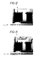
- Fig. 2 is an enlarged photograph of a resistor from Group I of resistors tested for a resistance shift after a laser scribing operation;
- Fig. 3 is an enlarged photograph of a resistor from Group II of resistors tested for a resistance shift after a laser scribing operation;
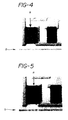
- Fig. 4 is an enlarged photograph of a resistor from Group III of resistors tested for a resistance shift after a laser scribing operation; and,
- Fig. 5 is an enlarged photograph of a resistor from Group IV of resistors tested for a resistance shift after a laser scribing operation.
- Referring to Figure 1, there is shown a flow diagram illustrating a method according to the present invention for forming a thick-
film circuit 10 having at least one thick-film resistor element 16 upon asubstrate 12 and laser scribing thesubstrate 12 to remove thecircuit 10 from the remaining portion of thesubstrate 12. - As shown in Fig. 1, thick-
film conductor lines 14 are formed on thesubstrate 12. The thick-film resistor element 16 is then formed on thesubstrate 12 and over a portion of theconductor lines 14. Thecircuit 10 may include a plurality ofconductor lines 14 and one ormore resistor elements 16. As can be seen, thesubstrate 12 is broken away, indicating that multiple thick-film circuits 10 are preferably formed on thesubstrate 12. - Preferably the
substrate 12 is a ceramic substrate such as a fired alumina substrate; although, other substrate materials such as SbN4, AIN, and quartz may be used. - The
conductor lines 14 may be screen printed onto thesubstrate 12, and subsequently dried and fired. The material for theconductor lines 14 may be selected from any one of the alloy families of gold, silver, palladium silvers, platinum gold or palladium golds. After theconductor lines 14 are printed onto thesubstrate 12, they are typically dried for about 20 minutes at 150°C, and subsequently fired through a belt furnace using a 30-60 minute cycle with 8-10 minutes at a peak temperature of 850°C. - The
resistor element 16 may be formed next, as shown in Fig. 1, using screen printing techniques. The material used in forming theresistor element 16 may be a resistor paste such as ruthenium dioxide paste. Other resistor materials containing Pd, carbon, or tantalum nitride may also be used. After theresistor element 16 is screen printed onto the substrate, it is dried and subsequently fired in a similar manner to that of theconductor lines 14. - After the
resistor element 16 is formed on thesubstrate 12, it may be laser trimmed in a known manner, as shown in Fig. 1, in order to increase the resistance value thereof. A laser beam projector (not shown) which produces a beam 20 is employed to evaporate a portion of the resistance material of theresistor element 16, thereby increasing the resistance value thereof. - Following the laser trimming step and prior to the laser scribing step, a
protective material 18 is coated onto theresistor element 16 and dried. The protective material preferably comprises an organic polymer such as T-type ethyl cellulose which is a 49.6% minimum ethoxyl content cellulose, designated by CAS Abstract # 9004-57-3. After coating, the ethyl cellulose coating is preferably dried for 5-10 minutes at a temperature of 150°C. The ethyl cellulose coating serves to protect theresistor element 16 from hot- slag substrate material generated during the laser scribing step by acting as a barrier to any substrate material sputtered onto theelement 16. - After the protective coating is applied onto the
resistor element 16, thesubstrate 12 is laser scribed by a laser beam projector (not shown) to separate the thick-film circuit 10 from the remaining portion of thesubstrate 12. Preferably, the substrate is scribed from thetopside 24 of thesubstrate 12. The laser projector produces abeam 22 which creates scribes S or score lines in the substrate, each having a depth equal to approximately one-third the thickness of thesubstrate 12. After the scribe lines S are formed in thesubstrate 12, thecircuit 10 is then be broken away from the remaining portion of thesubstrate 12. This may be done manually. Preferably, a plurality of thick-film circuits 10 are formed on thesubstrate 12 and are separated from one another during the laser scribing operation. - After the laser scribing operation, the
resistor element 16 is washed to remove from its outer surface theprotective material 18 and any substrate material trapped in theprotective material 18. If the protective material is ethyl cellulose, a solvent comprising an alcohol may be used to wash the material 18 from theresistor element 16. A further known solvent which is sold under the tradename PRELETE by Dow Chemical Company may alternatively be used to wash theresistor element 16. - The following example is given to illustrate certain preferred details of the invention, it being understood that the details of the example are not to be taken as in any way limiting the invention thereto.
- Four test groups were provided. Each group included 24 thick-film circuits having at least one resistor element formed thereon. Each of the 24 circuits of each group were formed on 24 separate substrates. One resistor element was tested from each circuit in each group to test the resistance shift of the resistor after its respective substrate was laser scribed. Substantially all of the resistance shifts were upward shifts, i.e., the resistance value of the resistor increased.
- In group I, the resistor elements were untrimmed and uncoated before laser scribing. In group II, the resistor elements were untrimmed but were coated with ethyl cellulose before laser scribing. In group III, the resistor elements were laser trimmed and uncoated before laser scribing. In Group IV, the resistor elements were laser trimmed and coated with ethyl cellulose before laser scribing. The resistor elements in each group were formed from ruthenium dioxide resistor paste. The untrimmed resistors were 40 KOHM value resistors and the trimmed resistors were 60 KOHM value resistors. The resistor elements were formed upon a 96% alumina substrate. The substrate also included conductor lines thereon formed from silver palladium paste.
- Each resistor was tested for resistance shift after laser scribing and after 24 hours of thermal ageing at 125°C. The resistance shifts measured from the untrimmed resistors of groups I and II were averaged for each group and compared to the desired value of 40 KOHM. Likewise, the resistance shifts measured from the trimmed resistors of groups III and IV were averaged for each group and compared to the desired value of 60 KOHM.
- The results are shown in Table 1 below:

- The coated resistor elements from groups II and IV, measured before thermal ageing, had average resistance shifts of <.01 KOHM and .019 KOHM, respectively. The uncoated resistor elements from groups I and III, measured before thermal ageing, had average resistance shifts of .044 KOHM and .097 KOHM, respectively. The coated resistor elements from groups II and IV, measured after 24 hours of thermal ageing at 125°C, had average resistance shifts of .03 KOHM and .054 KOHM, respectively. The uncoated resistor elements from groups I and III, measured after thermal ageing, had average resistance shifts of .064 KOHM and .139 KOHM, respectively. Thus, the average shift in resistance for the coated, untrimmed resistors of group II was less than that of the non-coated, untrimmed resistors of group I, both before and after thermal ageing. Further, the average shift in resistance for the coated, trimmed resistors of group IV was less than that of the non-coated, trimmed resistors of group III, both before and after thermal ageing.
- Surface damage after laser scribing to a resistor element from groups I, II, III, and IV may be seen in Figures 2, 3, 4, and 5, respectively. The scribe lines are designated by the letter "S", while the resistors are designated by the letter "R". The straight, white lines on the resistors are scratches caused by hot-slag ceramic material and the white dotted areas are hot-slag ceramic particles. It should be apparent that the non-coated resistor elements from groups I and III, shown in Figs. 2 and 4, respectively, were damaged significantly more by hot- slag ceramic material than the coated resistors from groups II and IV, shown in Figs. 3 and 5, respectively.
- The results of Example I above lead to the following conclusions:
- 1) The thick-film untrimmed resistor elements coated with ethyl cellulose prior to laser scribing experienced an average resistance shift significantly less than the untrimmed resistor elements left uncoated during laser scribing, both before and after thermal ageing.
- 2) The thick-film trimmed resistor elements coated with ethyl cellulose prior to laser scribing experienced an average resistance shift significantly less than the trimmed resistor elements left uncoated during laser scribing, both before and after thermal ageing.
- 3) The thick-film resistor elements coated with ethyl cellulose prior to laser scribing experienced substantially no visual surface damage whereas the uncoated resistor elements experienced permanent microscopic surface damage, i.e., scratches.
- By the present invention, a method is provided for protecting a resistor element formed on a substrate during a laser scribing operation. The method comprises coating a protective material, preferably ethyl cellulose, onto the resistor element prior to the laser scribing operation to protect the resistor element from hot-slag substrate material generated during the laser scribing operation.
- Having described the invention in detail and by reference to preferred embodiments thereof, it will be apparent that modifications and variations are possible without departing from the scope of the invention defined in the appended claims. For example, it is contemplated that an ethyl cellulose coating may be used to protect other sensitive areas on a circuit board, such as sensitive sections of conductor lines, dielectric layers and the like. Further, it is contemplated that an ethyl cellulose coating may be employed to protect resistors or the like on multi- layered circuits. It is also contemplated that an ethyl cellulose coating may be employed as an environmental protectant for any circuit element formed or located on a circuit board.
Claims (9)
1. A method of laser scribing a substrate (12) having a thick-film circuit (10) formed thereon comprising the steps of, coating onto an outer surface of at least one portion (16) of said thick-film circuit a protective material (18) to protect said portion (16) from hot-slag substrate material generated during a laser scribing operation, laser scribing said substrate (12) to separate said thick-film circuit (10) from the remainder of said substrate (12), and, removing said protective material (18) from said outer surface of said portion (16).
2. A method of laser scribing a substrate as claimed in claim 1, wherein said at least one portion comprises at least one thick-film resistor.
3. A method of forming a thick-film circuit having at least one thick-film resistor upon a substrate comprising the steps of, printing said thick-film circuit having said at least one thick-film resistor onto said substrate, laser trimming said at least one thick-film resistor to increase the resistance value thereof, coating onto the outer surface of said resistor a protective material to protect said resistor from hot-slag substrate material generated during a laser scribing operation, laser scribing said substrate to separate said thick-film circuit from the remainder of said substrate, and removing said protective material from said outer surface of said resistor.
4. A method of forming a thick-film circuit as claimed in claim 3, wherein said step of printing said "thick-film circuit having at least one thick-film resistor onto said substrate comprises the steps of, printing conductor paste onto said substrate to form conductor lines thereon, and printing resistor paste onto said substrate to form said at least one thick-film resistor thereon.
5. A method of laser scribing a substrate as claimed in claim 3 and 4, wherein said thick-film circuit is printed on a topside of said substrate and said step of laser scribing said substrate to separate said thick-film circuit from the remainder of said substrate occurs on the topside of said substrate.
6. A method of laser scribing a substrate as claimed in any one of the preceding claims, wherein said substrate is a ceramic or aluminia substrate.
7. A method of laser scribing a substrate as claimed in any preceding claims, wherein said protective material comprises ethyl cellulose.
8. A method of laser scribing a substrate as claimed in Claim 7, wherein said ethyl cellulose is removed from said outer surface of said portion by washing with a solvent.
9. An intermediate product for use in the production of thick-film circuits comprising, a substrate, at least two conductor lines formed on said substrate, at least one resistor element formed on said substrate and over a portion of each of said two conductor lines, and a protective material formed over said resistor to protect said resistor from hot-slag substrate material generated during a laser scribing operation.
Applications Claiming Priority (2)
| Application Number | Priority Date | Filing Date | Title |
|---|---|---|---|
| US570063 | 1990-08-20 | ||
| US07/570,063 US5116641A (en) | 1990-08-20 | 1990-08-20 | Method for laser scribing substrates |
Publications (1)
| Publication Number | Publication Date |
|---|---|
| EP0472277A1 true EP0472277A1 (en) | 1992-02-26 |
Family
ID=24278057
Family Applications (1)
| Application Number | Title | Priority Date | Filing Date |
|---|---|---|---|
| EP91306048A Ceased EP0472277A1 (en) | 1990-08-20 | 1991-07-03 | Method for laser scribing substrates |
Country Status (3)
| Country | Link |
|---|---|
| US (1) | US5116641A (en) |
| EP (1) | EP0472277A1 (en) |
| JP (1) | JPH04233753A (en) |
Cited By (2)
| Publication number | Priority date | Publication date | Assignee | Title |
|---|---|---|---|---|
| GB2320137A (en) * | 1997-05-08 | 1998-06-10 | Yageo Corp | Method for fabrication of a thin film resisitor |
| EP1101228A1 (en) * | 1999-05-11 | 2001-05-23 | Motorola, Inc. | Polymer thick-film resistor printed on planar circuit board surface |
Families Citing this family (8)
| Publication number | Priority date | Publication date | Assignee | Title |
|---|---|---|---|---|
| DE4345586B4 (en) * | 1992-12-22 | 2009-04-23 | Denso Corp., Kariya-shi | Method for producing multiple thick-film substrates |
| US5928526A (en) * | 1997-04-29 | 1999-07-27 | Stellex Microwave Systems, Inc. | Method for manufacturing a substrate having an irregular shape |
| US6047463A (en) | 1998-06-12 | 2000-04-11 | Intermedics Inc. | Embedded trimmable resistors |
| US6631551B1 (en) * | 1998-06-26 | 2003-10-14 | Delphi Technologies, Inc. | Method of forming integral passive electrical components on organic circuit board substrates |
| US6240635B1 (en) * | 1998-11-20 | 2001-06-05 | International Business Machines Corporation | Printed circuit board scrap removal and printed circuit board fabrication process |
| WO2003082583A1 (en) | 2002-03-22 | 2003-10-09 | Ap Technoglass | Laser marking system |
| SG119230A1 (en) * | 2004-07-29 | 2006-02-28 | Micron Technology Inc | Interposer including at least one passive element at least partially defined by a recess formed therein method of manufacture system including same and wafer-scale interposer |
| US8290239B2 (en) * | 2005-10-21 | 2012-10-16 | Orbotech Ltd. | Automatic repair of electric circuits |
Citations (5)
| Publication number | Priority date | Publication date | Assignee | Title |
|---|---|---|---|---|
| US4486738A (en) * | 1982-02-16 | 1984-12-04 | General Electric Ceramics, Inc. | High reliability electrical components |
| EP0167198A1 (en) * | 1984-06-22 | 1986-01-08 | Laboratoires D'electronique Et De Physique Appliquee L.E.P. | Starting mixture for an isolating composition containing a lead glass, screen printing ink comprising such a mixture, and use of this ink for protecting hybrid microcircuits on ceramic substrates |
| US4694568A (en) * | 1982-01-07 | 1987-09-22 | North American Philips Corporation | Method of manufacturing chip resistors with edge around terminations |
| US4788523A (en) * | 1987-12-10 | 1988-11-29 | United States Of America | Viad chip resistor |
| EP0337412A2 (en) * | 1988-04-15 | 1989-10-18 | E.I. Du Pont De Nemours And Company | Encapsulant composition |
Family Cites Families (11)
| Publication number | Priority date | Publication date | Assignee | Title |
|---|---|---|---|---|
| US3066033A (en) * | 1960-07-29 | 1962-11-27 | American Cyanamid Co | Cellulose ester coating composition |
| US4082830A (en) * | 1972-05-10 | 1978-04-04 | W. R. Grace & Co. | Process of forming a protective coating and shipping the coating from the surface being protected when no longer required |
| US4071639A (en) * | 1975-10-22 | 1978-01-31 | Combustion Engineering, Inc. | Coating material and method |
| US4081653A (en) * | 1976-12-27 | 1978-03-28 | Western Electric Co., Inc. | Removal of thin films from substrates by laser induced explosion |
| US4301194A (en) * | 1979-05-04 | 1981-11-17 | Purex Corporation | Chemical milling maskant application process |
| US4288530A (en) * | 1979-10-15 | 1981-09-08 | Motorola, Inc. | Method of tuning apparatus by low power laser beam removal |
| US4352835A (en) * | 1981-07-01 | 1982-10-05 | Western Electric Co., Inc. | Masking portions of a substrate |
| US4783421A (en) * | 1985-04-15 | 1988-11-08 | Solarex Corporation | Method for manufacturing electrical contacts for a thin-film semiconductor device |
| JPS6240787A (en) * | 1985-08-16 | 1987-02-21 | New Japan Radio Co Ltd | Thick film chip resistor |
| US4931323A (en) * | 1987-12-10 | 1990-06-05 | Texas Instruments Incorporated | Thick film copper conductor patterning by laser |
| JPH02250390A (en) * | 1989-03-24 | 1990-10-08 | Ngk Insulators Ltd | Manufacture of ceramic board for feeding |
-
1990
- 1990-08-20 US US07/570,063 patent/US5116641A/en not_active Expired - Fee Related
-
1991
- 1991-07-03 EP EP91306048A patent/EP0472277A1/en not_active Ceased
- 1991-08-08 JP JP3199346A patent/JPH04233753A/en active Pending
Patent Citations (5)
| Publication number | Priority date | Publication date | Assignee | Title |
|---|---|---|---|---|
| US4694568A (en) * | 1982-01-07 | 1987-09-22 | North American Philips Corporation | Method of manufacturing chip resistors with edge around terminations |
| US4486738A (en) * | 1982-02-16 | 1984-12-04 | General Electric Ceramics, Inc. | High reliability electrical components |
| EP0167198A1 (en) * | 1984-06-22 | 1986-01-08 | Laboratoires D'electronique Et De Physique Appliquee L.E.P. | Starting mixture for an isolating composition containing a lead glass, screen printing ink comprising such a mixture, and use of this ink for protecting hybrid microcircuits on ceramic substrates |
| US4788523A (en) * | 1987-12-10 | 1988-11-29 | United States Of America | Viad chip resistor |
| EP0337412A2 (en) * | 1988-04-15 | 1989-10-18 | E.I. Du Pont De Nemours And Company | Encapsulant composition |
Non-Patent Citations (2)
| Title |
|---|
| PATENT ABSTRACTS OF JAPAN vol. 11, no. 224 (E-525)(2671) 21 July 1987, & JP-A-62 040787 (NEW JAPAN RADIO CO.LTD.) 21 February 1987, * |
| PATENT ABSTRACTS OF JAPAN vol. 14, no. 576 (E-1016) 21 December 1990, & JP-A-02 250390 (NGK INSULATORS LTD.) 08 October 1990, * |
Cited By (4)
| Publication number | Priority date | Publication date | Assignee | Title |
|---|---|---|---|---|
| GB2320137A (en) * | 1997-05-08 | 1998-06-10 | Yageo Corp | Method for fabrication of a thin film resisitor |
| GB2320137B (en) * | 1997-05-08 | 1998-11-18 | Yageo Corp | Method for fabrication of thin film resistor |
| EP1101228A1 (en) * | 1999-05-11 | 2001-05-23 | Motorola, Inc. | Polymer thick-film resistor printed on planar circuit board surface |
| EP1101228A4 (en) * | 1999-05-11 | 2007-11-07 | Motorola Inc | Polymer thick-film resistor printed on planar circuit board surface |
Also Published As
| Publication number | Publication date |
|---|---|
| US5116641A (en) | 1992-05-26 |
| JPH04233753A (en) | 1992-08-21 |
Similar Documents
| Publication | Publication Date | Title |
|---|---|---|
| US5116641A (en) | Method for laser scribing substrates | |
| EP1020909B1 (en) | Method for producing a thick-film hybrid circuit on a metal circuit board | |
| US4031272A (en) | Hybrid integrated circuit including thick film resistors and thin film conductors and technique for fabrication thereof | |
| US6120835A (en) | Process for manufacture of thick film hydrogen sensors | |
| US4740863A (en) | Current-limiting thin film termination for capacitors | |
| US5206624A (en) | Intermediate product for use in the production of thick-film circuits | |
| US5593722A (en) | Method of producing thick multi-layer substrates | |
| US6521355B1 (en) | Optical color tracer indentifier in metal paste that bleed to greensheet | |
| JP2526347B2 (en) | Encapsulant composition | |
| US5723073A (en) | Conductive paste containing 2-tetradecanol and ceramic circuit substrate using the same | |
| US4694568A (en) | Method of manufacturing chip resistors with edge around terminations | |
| EP0054101B1 (en) | Method and apparatus for monitoring solvent content of ceramic green sheets | |
| TWI237898B (en) | A thin film resistance manufacturing method | |
| JP3129170B2 (en) | Method of manufacturing rectangular thin film chip resistor | |
| JP3304130B2 (en) | Method of manufacturing rectangular thin film chip resistor | |
| JP3635669B2 (en) | Method for producing thick film multilayer substrate | |
| JPH04154104A (en) | Laminated ceramic capacitor | |
| JP2971605B2 (en) | Laminate | |
| JP3136682B2 (en) | Method for manufacturing multilayer wiring board | |
| EP0885458A1 (en) | Method for making electrical connections | |
| GB2393332A (en) | Method of fabricating a ceramic circuit board using conductor paste with chosen shrinkage properties. | |
| JPH01300592A (en) | Thick-film multilayer wiring board | |
| JP2005277436A (en) | Method of producing thick-film multi-layer substrates | |
| JP3719518B2 (en) | Method for producing thick film multilayer substrate | |
| JPH0575262A (en) | Manufacture of ceramic multilayer circuit board |
Legal Events
| Date | Code | Title | Description |
|---|---|---|---|
| PUAI | Public reference made under article 153(3) epc to a published international application that has entered the european phase |
Free format text: ORIGINAL CODE: 0009012 |
|
| AK | Designated contracting states |
Kind code of ref document: A1 Designated state(s): DE FR GB NL |
|
| 17P | Request for examination filed |
Effective date: 19920730 |
|
| 17Q | First examination report despatched |
Effective date: 19941215 |
|
| GRAG | Despatch of communication of intention to grant |
Free format text: ORIGINAL CODE: EPIDOS AGRA |
|
| STAA | Information on the status of an ep patent application or granted ep patent |
Free format text: STATUS: THE APPLICATION HAS BEEN REFUSED |
|
| 18R | Application refused |
Effective date: 19960706 |