EP0471982A1 - Système de montage pour unités électriques de fonction, notamment pour la technique de données - Google Patents
Système de montage pour unités électriques de fonction, notamment pour la technique de données Download PDFInfo
- Publication number
- EP0471982A1 EP0471982A1 EP91111843A EP91111843A EP0471982A1 EP 0471982 A1 EP0471982 A1 EP 0471982A1 EP 91111843 A EP91111843 A EP 91111843A EP 91111843 A EP91111843 A EP 91111843A EP 0471982 A1 EP0471982 A1 EP 0471982A1
- Authority
- EP
- European Patent Office
- Prior art keywords
- contact
- functional units
- pads
- circuit boards
- cooling plates
- Prior art date
- Legal status (The legal status is an assumption and is not a legal conclusion. Google has not performed a legal analysis and makes no representation as to the accuracy of the status listed.)
- Granted
Links
Images
Classifications
-
- H—ELECTRICITY
- H05—ELECTRIC TECHNIQUES NOT OTHERWISE PROVIDED FOR
- H05K—PRINTED CIRCUITS; CASINGS OR CONSTRUCTIONAL DETAILS OF ELECTRIC APPARATUS; MANUFACTURE OF ASSEMBLAGES OF ELECTRICAL COMPONENTS
- H05K7/00—Constructional details common to different types of electric apparatus
- H05K7/14—Mounting supporting structure in casing or on frame or rack
- H05K7/1438—Back panels or connecting means therefor; Terminals; Coding means to avoid wrong insertion
-
- H—ELECTRICITY
- H01—ELECTRIC ELEMENTS
- H01L—SEMICONDUCTOR DEVICES NOT COVERED BY CLASS H10
- H01L23/00—Details of semiconductor or other solid state devices
- H01L23/34—Arrangements for cooling, heating, ventilating or temperature compensation ; Temperature sensing arrangements
- H01L23/46—Arrangements for cooling, heating, ventilating or temperature compensation ; Temperature sensing arrangements involving the transfer of heat by flowing fluids
- H01L23/473—Arrangements for cooling, heating, ventilating or temperature compensation ; Temperature sensing arrangements involving the transfer of heat by flowing fluids by flowing liquids
-
- H—ELECTRICITY
- H01—ELECTRIC ELEMENTS
- H01L—SEMICONDUCTOR DEVICES NOT COVERED BY CLASS H10
- H01L2924/00—Indexing scheme for arrangements or methods for connecting or disconnecting semiconductor or solid-state bodies as covered by H01L24/00
- H01L2924/0001—Technical content checked by a classifier
- H01L2924/0002—Not covered by any one of groups H01L24/00, H01L24/00 and H01L2224/00
-
- H—ELECTRICITY
- H01—ELECTRIC ELEMENTS
- H01L—SEMICONDUCTOR DEVICES NOT COVERED BY CLASS H10
- H01L2924/00—Indexing scheme for arrangements or methods for connecting or disconnecting semiconductor or solid-state bodies as covered by H01L24/00
- H01L2924/30—Technical effects
- H01L2924/301—Electrical effects
- H01L2924/3011—Impedance
Definitions
- the invention relates to an installation system for electrical functional units, in particular data technology, consisting of an alternating sequence of cooling plates provided with cooling channels for a coolant and with plated-through holes and of printed circuit boards constructed in micro-wiring technology, the contact surfaces (contact pads) on their two surfaces for contacting the connection contact surfaces Have (connection pads) of integrated components, which in turn rest with their side not provided with connection pads on the cooling plates and in which the operating and signal voltages are supplied to the functional units from the outside via plugs.
- the multi-layer printed circuit boards with components, in particular chips are arranged side by side on one level in a grid frame provided with corresponding recesses, each of these printed circuit boards being assigned its own cooling plate, which is made of good heat-dissipating material, on the component-carrying side of the printed circuit board.
- a common circuit board through which coolant flows and which contacts all the individual cooling plates ensures that the heat supplied to the individual cooling plates is dissipated from the circuit boards.
- the connection of the printed circuit boards with a wiring plate attached to the back of the lattice frame is made using pressure connectors that are located on the back of the printed circuit boards.
- German patent application P 39 35 047.9 it has already been proposed in German patent application P 39 35 047.9 to arrange a plurality of printed circuit boards and cooling plates in parallel behind or on top of one another, so that they form a cuboid.
- the cooling plates are provided with cooling channels and openings perpendicular to them, in which resilient pressure contacts for the wiring of the printed circuit boards are arranged with one another.
- connector plates with cutouts for receiving cable plugs for the signal supply are provided, operating voltages being introduced on the other two sides of the cuboid and the coolant supply and the coolant supply for the cooling plates being introduced on the third side pairs. This achieves three-dimensional wiring within the functional unit and thus further compression of components per unit volume.
- the object of the present invention is to provide a built-in system for electrical functional units, in particular for data technology, in which the space-performance ratio is further optimized.
- the installation system is designed such that the connection pads of the integrated components are in direct contact with one another with the contact pads of the printed circuit boards via contact mats.
- the invention can be designed in such a way that recesses are provided between the contact pads of the printed circuit boards up to the next metal level of the printed circuit board, in which discrete wires for change wiring can be laid, that the discrete wires can be connected to connection spots etched free on this next metal level, which in turn can be connected are connected via vias to the contact pads on the printed circuit board surfaces.
- next metal level is set to zero volt potential, a defined characteristic impedance can be created with the change wiring.
- connection pads for the integrated components and the connection points for the plated-through holes on the cooling plates are at the same level. This means that a continuous contact mat can be used for all connections.
- the cooling effectiveness can be increased further since the shortest paths from the heat source (chip) to the heat sink (cooling plate), which can either contain water or liquid nitrogen as cooling liquid, are produced.
- the heat transfer from the integrated component to the cooling plate is also minimized because of the direct mounting of the chip on the cooling plate.
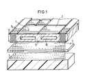
- FIG. 1 A partial area of a functional unit is shown in FIG.
- the integrated components 2 are in direct contact with their side of the cooling plate 9 facing away from the contact, which is provided with cooling channels 10. These modules 2 can either be fixed (e.g. adhesive or soldering) to the cooling plate 9, to achieve very good heat transfer, or they can only be pressed onto the latter, which facilitates the interchangeability that may be required.
- the cooling plates are provided with vias 12 on the sides. Since both the contacts for the plated-through holes and the connection contacts 1 of the integrated modules 2 lie on the same contact level, simple connection of the integrated modules 2 lying on both sides on the cooling plate 9 is possible in this way.
- micro-wiring 4 - The contacting of the integrated modules 2 with the printed circuit board 4 constructed in micro-wiring - hereinafter referred to as micro-wiring 4 - with which the wiring of the integrated modules 2 is carried out on one side in each case takes place via the contact mat 5.
- Such contact mats are already known.
- the sandwich-like structure of such a functional unit can now be continued as desired on both sides, so that a contact mat 5 and then a micro-wiring 4 comes to rest on the top of the section shown in FIG.
- a contact mat 5 then makes contact with the next component level via the microwiring 4, the components in turn being arranged on a further cooling plate.
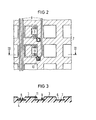
- FIG. 2 shows a plan view of the printed circuit board 4 in micro-wiring, the connections of which consist of the contact pads 3, to which the connections to the connection pads 1 of the components 2 are guided via the contact mat 5, not shown, above.
- These contact pads 3 are created by free etching on the surface of the printed circuit boards 4. Between these contact pads 3 there are then depressions 6, e.g. etched with laser, which extend to the nearest metal layer 7. This metal layer 7 is at zero volt potential. On this metal layer 7, the direct wiring 8 is laid on the zero volt level between the component connections in order to achieve a controlled characteristic impedance. At this lower level, the change wiring is contacted to etched-off contact pads 13. The electrical connection of these contact pads 13 to the component connection pads 3 takes place via the parallel vias 11.
- FIG. 3 A cross section in FIG. 3 shows the contact pads 3 and the provided depressions 6, in which the discrete wiring can run, as well as the plated-through holes 11 and the zero volt metal surface 7.
Landscapes
- Engineering & Computer Science (AREA)
- Microelectronics & Electronic Packaging (AREA)
- Physics & Mathematics (AREA)
- Condensed Matter Physics & Semiconductors (AREA)
- General Physics & Mathematics (AREA)
- Computer Hardware Design (AREA)
- Power Engineering (AREA)
- Cooling Or The Like Of Semiconductors Or Solid State Devices (AREA)
- Cooling Or The Like Of Electrical Apparatus (AREA)
- Structures For Mounting Electric Components On Printed Circuit Boards (AREA)
- Small-Scale Networks (AREA)
Priority Applications (1)
| Application Number | Priority Date | Filing Date | Title |
|---|---|---|---|
| AT9191111843T ATE105458T1 (de) | 1990-08-03 | 1991-07-16 | Einbausystem fuer elektrische funktionseinheiten insbesondere fuer die datentechnik. |
Applications Claiming Priority (2)
| Application Number | Priority Date | Filing Date | Title |
|---|---|---|---|
| DE4024737 | 1990-08-03 | ||
| DE4024737 | 1990-08-03 |
Publications (2)
| Publication Number | Publication Date |
|---|---|
| EP0471982A1 true EP0471982A1 (fr) | 1992-02-26 |
| EP0471982B1 EP0471982B1 (fr) | 1994-05-04 |
Family
ID=6411624
Family Applications (1)
| Application Number | Title | Priority Date | Filing Date |
|---|---|---|---|
| EP91111843A Expired - Lifetime EP0471982B1 (fr) | 1990-08-03 | 1991-07-16 | Système de montage pour unités électriques de fonction, notamment pour la technique de données |
Country Status (5)
| Country | Link |
|---|---|
| US (1) | US5153814A (fr) |
| EP (1) | EP0471982B1 (fr) |
| JP (1) | JPH088423B2 (fr) |
| AT (1) | ATE105458T1 (fr) |
| DE (1) | DE59101555D1 (fr) |
Cited By (1)
| Publication number | Priority date | Publication date | Assignee | Title |
|---|---|---|---|---|
| EP0762818A2 (fr) * | 1995-09-11 | 1997-03-12 | International Business Machines Corporation | Dispositif pour réaliser une connexion à une plaquette de circuit |
Families Citing this family (16)
| Publication number | Priority date | Publication date | Assignee | Title |
|---|---|---|---|---|
| EP0666595B1 (fr) * | 1994-02-07 | 1998-08-19 | Siemens Aktiengesellschaft | Procédé pour la fabrication d'un dispositif d'un circuit intégré cubique |
| US6392296B1 (en) | 1998-08-31 | 2002-05-21 | Micron Technology, Inc. | Silicon interposer with optical connections |
| US6586835B1 (en) * | 1998-08-31 | 2003-07-01 | Micron Technology, Inc. | Compact system module with built-in thermoelectric cooling |
| US6281042B1 (en) | 1998-08-31 | 2001-08-28 | Micron Technology, Inc. | Structure and method for a high performance electronic packaging assembly |
| US6219237B1 (en) | 1998-08-31 | 2001-04-17 | Micron Technology, Inc. | Structure and method for an electronic assembly |
| US6255852B1 (en) | 1999-02-09 | 2001-07-03 | Micron Technology, Inc. | Current mode signal interconnects and CMOS amplifier |
| US7554829B2 (en) | 1999-07-30 | 2009-06-30 | Micron Technology, Inc. | Transmission lines for CMOS integrated circuits |
| US6464513B1 (en) | 2000-01-05 | 2002-10-15 | Micron Technology, Inc. | Adapter for non-permanently connecting integrated circuit devices to multi-chip modules and method of using same |
| US6407566B1 (en) | 2000-04-06 | 2002-06-18 | Micron Technology, Inc. | Test module for multi-chip module simulation testing of integrated circuit packages |
| US6540525B1 (en) * | 2001-08-17 | 2003-04-01 | High Connection Density, Inc. | High I/O stacked modules for integrated circuits |
| US7045889B2 (en) | 2001-08-21 | 2006-05-16 | Micron Technology, Inc. | Device for establishing non-permanent electrical connection between an integrated circuit device lead element and a substrate |
| US7049693B2 (en) * | 2001-08-29 | 2006-05-23 | Micron Technology, Inc. | Electrical contact array for substrate assemblies |
| US7101770B2 (en) | 2002-01-30 | 2006-09-05 | Micron Technology, Inc. | Capacitive techniques to reduce noise in high speed interconnections |
| US7235457B2 (en) | 2002-03-13 | 2007-06-26 | Micron Technology, Inc. | High permeability layered films to reduce noise in high speed interconnects |
| DE10229711B4 (de) * | 2002-07-02 | 2009-09-03 | Curamik Electronics Gmbh | Halbleitermodul mit Mikrokühler |
| US7432592B2 (en) * | 2005-10-13 | 2008-10-07 | Intel Corporation | Integrated micro-channels for 3D through silicon architectures |
Citations (5)
| Publication number | Priority date | Publication date | Assignee | Title |
|---|---|---|---|---|
| GB1178566A (en) * | 1966-06-13 | 1970-01-21 | Ibm | Improvements in and relating to Electronic Circuit Packages |
| EP0113794A1 (fr) * | 1982-12-21 | 1984-07-25 | Siemens Aktiengesellschaft | Support pour des plaquettes de composants |
| EP0268260A1 (fr) * | 1986-11-18 | 1988-05-25 | International Business Machines Corporation | Support à film flexible pour puce avec des condensateurs de découplage |
| US4933808A (en) * | 1989-05-11 | 1990-06-12 | Westinghouse Electric Corp. | Solderless printed wiring board module and multi-module assembly |
| EP0428859A2 (fr) * | 1989-10-20 | 1991-05-29 | Siemens Nixdorf Informationssysteme Aktiengesellschaft | Unité fonctionnelle électrique pour traitement de donnÀ©es |
Family Cites Families (11)
| Publication number | Priority date | Publication date | Assignee | Title |
|---|---|---|---|---|
| DE428859C (de) * | 1925-07-06 | 1926-05-14 | Eberhard Legeler Dr | Verfahren zur kontinuierlichen Abscheidung von Schwefel aus Schwefelloesungen |
| US4016138A (en) * | 1973-02-08 | 1977-04-05 | Michigan Chemical Corporation | Plastic compositions |
| US4060113A (en) * | 1974-07-03 | 1977-11-29 | Ryuzo Matsushima | Tightening device for threaded screw part |
| US4019098A (en) * | 1974-11-25 | 1977-04-19 | Sundstrand Corporation | Heat pipe cooling system for electronic devices |
| US4037270A (en) * | 1976-05-24 | 1977-07-19 | Control Data Corporation | Circuit packaging and cooling |
| US4597617A (en) * | 1984-03-19 | 1986-07-01 | Tektronix, Inc. | Pressure interconnect package for integrated circuits |
| EP0204568A3 (fr) * | 1985-06-05 | 1988-07-27 | Harry Arthur Hele Spence-Bate | Composants de circuits à basse puissance |
| JPS6212991U (fr) * | 1985-07-05 | 1987-01-26 | ||
| JPS63192256A (ja) * | 1987-02-04 | 1988-08-09 | Nec Corp | 集積回路の冷却構造 |
| US4953060A (en) * | 1989-05-05 | 1990-08-28 | Ncr Corporation | Stackable integrated circuit chip package with improved heat removal |
| US5014117A (en) * | 1990-03-30 | 1991-05-07 | International Business Machines Corporation | High conduction flexible fin cooling module |
-
1991
- 1991-07-16 AT AT9191111843T patent/ATE105458T1/de not_active IP Right Cessation
- 1991-07-16 EP EP91111843A patent/EP0471982B1/fr not_active Expired - Lifetime
- 1991-07-16 DE DE59101555T patent/DE59101555D1/de not_active Expired - Fee Related
- 1991-07-18 US US07/732,482 patent/US5153814A/en not_active Expired - Fee Related
- 1991-07-29 JP JP3212655A patent/JPH088423B2/ja not_active Expired - Lifetime
Patent Citations (5)
| Publication number | Priority date | Publication date | Assignee | Title |
|---|---|---|---|---|
| GB1178566A (en) * | 1966-06-13 | 1970-01-21 | Ibm | Improvements in and relating to Electronic Circuit Packages |
| EP0113794A1 (fr) * | 1982-12-21 | 1984-07-25 | Siemens Aktiengesellschaft | Support pour des plaquettes de composants |
| EP0268260A1 (fr) * | 1986-11-18 | 1988-05-25 | International Business Machines Corporation | Support à film flexible pour puce avec des condensateurs de découplage |
| US4933808A (en) * | 1989-05-11 | 1990-06-12 | Westinghouse Electric Corp. | Solderless printed wiring board module and multi-module assembly |
| EP0428859A2 (fr) * | 1989-10-20 | 1991-05-29 | Siemens Nixdorf Informationssysteme Aktiengesellschaft | Unité fonctionnelle électrique pour traitement de donnÀ©es |
Cited By (2)
| Publication number | Priority date | Publication date | Assignee | Title |
|---|---|---|---|---|
| EP0762818A2 (fr) * | 1995-09-11 | 1997-03-12 | International Business Machines Corporation | Dispositif pour réaliser une connexion à une plaquette de circuit |
| EP0762818A3 (fr) * | 1995-09-11 | 1997-05-14 | Ibm | Dispositif pour réaliser une connexion à une plaquette de circuit |
Also Published As
| Publication number | Publication date |
|---|---|
| EP0471982B1 (fr) | 1994-05-04 |
| US5153814A (en) | 1992-10-06 |
| ATE105458T1 (de) | 1994-05-15 |
| JPH04233795A (ja) | 1992-08-21 |
| DE59101555D1 (de) | 1994-06-09 |
| JPH088423B2 (ja) | 1996-01-29 |
Similar Documents
| Publication | Publication Date | Title |
|---|---|---|
| EP0471982B1 (fr) | Système de montage pour unités électriques de fonction, notamment pour la technique de données | |
| DE1591199C2 (fr) | ||
| DE4015788C2 (de) | Baugruppe | |
| AT398254B (de) | Chipträger sowie anordnung von solchen chipträgern | |
| DE10240730B4 (de) | Leiterplatte, Speichermodul und Herstellungsverfahren | |
| CH667562A5 (de) | Verfahren zum aendern einer elektrischen flachbaugruppe. | |
| DE4305793A1 (de) | Leistungsmodul | |
| DE2843710A1 (de) | Mehrlagige flexible schaltungsplattenanordnung und verfahren zu ihrer herstellung | |
| EP0106990A1 (fr) | Elément pour faire contact entre des plaquettes à circuit imprimé | |
| DE69929337T2 (de) | Gedruckte leiterplatteneinheit, hierarchisches montagehilfssubstrat und elektronischer apparat | |
| DE69936189T2 (de) | Elektrischer leiter mit als flanschen und geätzte rillen geformter oberflächenstruktur | |
| DE3935047C2 (fr) | ||
| DE3212592A1 (de) | Kuehleinrichtung fuer geraete der nachrichtentechnik | |
| EP0153990A1 (fr) | Module plat | |
| DE3330466A1 (de) | Anordnung mit hoher packungsdichte von integrierten schaltungen | |
| DE19805492C2 (de) | Leiterplatte | |
| DE60201537T2 (de) | Elektrische verbindungsanordnung für elektronische bauteile | |
| DE2929050A1 (de) | Mehrschichtige gedruckte leiterplatte und verfahren zu ihrer auslegung | |
| EP0238712A1 (fr) | Matrice de commutateur commandée | |
| EP0073489A2 (fr) | Module électrique | |
| DE3209699C2 (de) | Universal-Leiterplatte | |
| DE2815646A1 (de) | Tragevorrichtung fuer elektronische schaltungen | |
| DE3411707A1 (de) | Rueckwandverdrahtung fuer einschiebbare elektrische baugruppen | |
| DE3134385A1 (de) | Elektrische baugruppe mit mehreren parallelen leiterplatten | |
| DE4305147C2 (de) | Elektrisches Gerät mit einer Vorrichtung zur Ableitung von Wärme von elektrischen Bauelementen |
Legal Events
| Date | Code | Title | Description |
|---|---|---|---|
| PUAI | Public reference made under article 153(3) epc to a published international application that has entered the european phase |
Free format text: ORIGINAL CODE: 0009012 |
|
| AK | Designated contracting states |
Kind code of ref document: A1 Designated state(s): AT BE CH DE FR GB IT LI NL |
|
| 17P | Request for examination filed |
Effective date: 19920325 |
|
| 17Q | First examination report despatched |
Effective date: 19930818 |
|
| GRAA | (expected) grant |
Free format text: ORIGINAL CODE: 0009210 |
|
| AK | Designated contracting states |
Kind code of ref document: B1 Designated state(s): AT BE CH DE FR GB IT LI NL |
|
| REF | Corresponds to: |
Ref document number: 105458 Country of ref document: AT Date of ref document: 19940515 Kind code of ref document: T |
|
| REF | Corresponds to: |
Ref document number: 59101555 Country of ref document: DE Date of ref document: 19940609 |
|
| PGFP | Annual fee paid to national office [announced via postgrant information from national office to epo] |
Ref country code: BE Payment date: 19940714 Year of fee payment: 4 |
|
| PGFP | Annual fee paid to national office [announced via postgrant information from national office to epo] |
Ref country code: FR Payment date: 19940725 Year of fee payment: 4 |
|
| ITF | It: translation for a ep patent filed |
Owner name: STUDIO JAUMANN |
|
| PGFP | Annual fee paid to national office [announced via postgrant information from national office to epo] |
Ref country code: NL Payment date: 19940731 Year of fee payment: 4 |
|
| GBT | Gb: translation of ep patent filed (gb section 77(6)(a)/1977) |
Effective date: 19940711 |
|
| ET | Fr: translation filed | ||
| PGFP | Annual fee paid to national office [announced via postgrant information from national office to epo] |
Ref country code: DE Payment date: 19940915 Year of fee payment: 4 |
|
| PGFP | Annual fee paid to national office [announced via postgrant information from national office to epo] |
Ref country code: CH Payment date: 19941017 Year of fee payment: 4 |
|
| PLBE | No opposition filed within time limit |
Free format text: ORIGINAL CODE: 0009261 |
|
| STAA | Information on the status of an ep patent application or granted ep patent |
Free format text: STATUS: NO OPPOSITION FILED WITHIN TIME LIMIT |
|
| 26N | No opposition filed | ||
| PGFP | Annual fee paid to national office [announced via postgrant information from national office to epo] |
Ref country code: GB Payment date: 19950622 Year of fee payment: 5 |
|
| PGFP | Annual fee paid to national office [announced via postgrant information from national office to epo] |
Ref country code: AT Payment date: 19950628 Year of fee payment: 5 |
|
| PG25 | Lapsed in a contracting state [announced via postgrant information from national office to epo] |
Ref country code: LI Effective date: 19950731 Ref country code: CH Effective date: 19950731 Ref country code: BE Effective date: 19950731 |
|
| BERE | Be: lapsed |
Owner name: SIEMENS NIXDORF INFORMATIONSSYSTEME A.G. Effective date: 19950731 |
|
| PG25 | Lapsed in a contracting state [announced via postgrant information from national office to epo] |
Ref country code: NL Effective date: 19960201 |
|
| REG | Reference to a national code |
Ref country code: CH Ref legal event code: PL |
|
| NLV4 | Nl: lapsed or anulled due to non-payment of the annual fee |
Effective date: 19960201 |
|
| PG25 | Lapsed in a contracting state [announced via postgrant information from national office to epo] |
Ref country code: DE Effective date: 19960402 |
|
| PG25 | Lapsed in a contracting state [announced via postgrant information from national office to epo] |
Ref country code: FR Effective date: 19960430 |
|
| REG | Reference to a national code |
Ref country code: FR Ref legal event code: ST |
|
| REG | Reference to a national code |
Ref country code: FR Ref legal event code: ST |
|
| REG | Reference to a national code |
Ref country code: FR Ref legal event code: ST |
|
| PG25 | Lapsed in a contracting state [announced via postgrant information from national office to epo] |
Ref country code: GB Effective date: 19960716 Ref country code: AT Effective date: 19960716 |
|
| GBPC | Gb: european patent ceased through non-payment of renewal fee |
Effective date: 19960716 |
|
| PG25 | Lapsed in a contracting state [announced via postgrant information from national office to epo] |
Ref country code: IT Free format text: LAPSE BECAUSE OF NON-PAYMENT OF DUE FEES;WARNING: LAPSES OF ITALIAN PATENTS WITH EFFECTIVE DATE BEFORE 2007 MAY HAVE OCCURRED AT ANY TIME BEFORE 2007. THE CORRECT EFFECTIVE DATE MAY BE DIFFERENT FROM THE ONE RECORDED. Effective date: 20050716 |