EP0470692A2 - Method and apparatus for measuring a deep inpurity level of a semiconductor crystal - Google Patents
Method and apparatus for measuring a deep inpurity level of a semiconductor crystal Download PDFInfo
- Publication number
- EP0470692A2 EP0470692A2 EP91304408A EP91304408A EP0470692A2 EP 0470692 A2 EP0470692 A2 EP 0470692A2 EP 91304408 A EP91304408 A EP 91304408A EP 91304408 A EP91304408 A EP 91304408A EP 0470692 A2 EP0470692 A2 EP 0470692A2
- Authority
- EP
- European Patent Office
- Prior art keywords
- specimen
- signal
- minority carriers
- microwave
- impurity level
- Prior art date
- Legal status (The legal status is an assumption and is not a legal conclusion. Google has not performed a legal analysis and makes no representation as to the accuracy of the status listed.)
- Withdrawn
Links
- 238000000034 method Methods 0.000 title claims abstract description 51
- 239000004065 semiconductor Substances 0.000 title claims abstract description 22
- 239000013078 crystal Substances 0.000 title description 3
- 239000012535 impurity Substances 0.000 claims abstract description 35
- 239000000969 carrier Substances 0.000 claims abstract description 20
- 230000008859 change Effects 0.000 claims abstract description 10
- 238000010168 coupling process Methods 0.000 claims abstract description 7
- 230000008878 coupling Effects 0.000 claims abstract description 6
- 238000005859 coupling reaction Methods 0.000 claims abstract description 6
- 230000001678 irradiating effect Effects 0.000 claims abstract description 6
- 239000000523 sample Substances 0.000 claims description 12
- 238000001514 detection method Methods 0.000 claims description 7
- 230000001360 synchronised effect Effects 0.000 claims description 4
- 230000002123 temporal effect Effects 0.000 claims description 4
- 230000008569 process Effects 0.000 abstract description 10
- 238000005215 recombination Methods 0.000 abstract description 5
- 230000006798 recombination Effects 0.000 abstract description 5
- 235000012431 wafers Nutrition 0.000 description 21
- 238000005259 measurement Methods 0.000 description 16
- 230000001066 destructive effect Effects 0.000 description 7
- IJGRMHOSHXDMSA-UHFFFAOYSA-N Atomic nitrogen Chemical compound N#N IJGRMHOSHXDMSA-UHFFFAOYSA-N 0.000 description 6
- 229910052751 metal Inorganic materials 0.000 description 5
- 239000002184 metal Substances 0.000 description 5
- 238000001816 cooling Methods 0.000 description 4
- 230000005284 excitation Effects 0.000 description 4
- 229910052775 Thulium Inorganic materials 0.000 description 3
- 238000004458 analytical method Methods 0.000 description 3
- 230000008033 biological extinction Effects 0.000 description 3
- 230000015572 biosynthetic process Effects 0.000 description 3
- 238000010586 diagram Methods 0.000 description 3
- 239000007788 liquid Substances 0.000 description 3
- 229910052757 nitrogen Inorganic materials 0.000 description 3
- 239000000758 substrate Substances 0.000 description 3
- XUIMIQQOPSSXEZ-UHFFFAOYSA-N Silicon Chemical compound [Si] XUIMIQQOPSSXEZ-UHFFFAOYSA-N 0.000 description 2
- 230000004913 activation Effects 0.000 description 2
- 230000002411 adverse Effects 0.000 description 2
- 238000010276 construction Methods 0.000 description 2
- 238000002474 experimental method Methods 0.000 description 2
- 238000010438 heat treatment Methods 0.000 description 2
- 230000006872 improvement Effects 0.000 description 2
- 230000006698 induction Effects 0.000 description 2
- 238000000691 measurement method Methods 0.000 description 2
- 230000007246 mechanism Effects 0.000 description 2
- 229910021421 monocrystalline silicon Inorganic materials 0.000 description 2
- 238000012545 processing Methods 0.000 description 2
- 239000010453 quartz Substances 0.000 description 2
- 238000005070 sampling Methods 0.000 description 2
- 229910052710 silicon Inorganic materials 0.000 description 2
- 239000010703 silicon Substances 0.000 description 2
- VYPSYNLAJGMNEJ-UHFFFAOYSA-N silicon dioxide Inorganic materials O=[Si]=O VYPSYNLAJGMNEJ-UHFFFAOYSA-N 0.000 description 2
- 239000004809 Teflon Substances 0.000 description 1
- 229920006362 Teflon® Polymers 0.000 description 1
- QVGXLLKOCUKJST-UHFFFAOYSA-N atomic oxygen Chemical compound [O] QVGXLLKOCUKJST-UHFFFAOYSA-N 0.000 description 1
- 238000009614 chemical analysis method Methods 0.000 description 1
- 229910052802 copper Inorganic materials 0.000 description 1
- 230000002542 deteriorative effect Effects 0.000 description 1
- 230000000694 effects Effects 0.000 description 1
- 238000010894 electron beam technology Methods 0.000 description 1
- 238000011156 evaluation Methods 0.000 description 1
- 229920002313 fluoropolymer Polymers 0.000 description 1
- 239000007789 gas Substances 0.000 description 1
- 229910052737 gold Inorganic materials 0.000 description 1
- 238000003780 insertion Methods 0.000 description 1
- 230000037431 insertion Effects 0.000 description 1
- 229910052742 iron Inorganic materials 0.000 description 1
- 238000004519 manufacturing process Methods 0.000 description 1
- 238000013507 mapping Methods 0.000 description 1
- 150000002739 metals Chemical class 0.000 description 1
- 229910052759 nickel Inorganic materials 0.000 description 1
- 239000001301 oxygen Substances 0.000 description 1
- 229910052760 oxygen Inorganic materials 0.000 description 1
- 239000002245 particle Substances 0.000 description 1
- 230000004044 response Effects 0.000 description 1
- 230000001052 transient effect Effects 0.000 description 1
- 238000002834 transmittance Methods 0.000 description 1
- 229910052721 tungsten Inorganic materials 0.000 description 1
Images


Classifications
-
- G—PHYSICS
- G01—MEASURING; TESTING
- G01R—MEASURING ELECTRIC VARIABLES; MEASURING MAGNETIC VARIABLES
- G01R31/00—Arrangements for testing electric properties; Arrangements for locating electric faults; Arrangements for electrical testing characterised by what is being tested not provided for elsewhere
- G01R31/26—Testing of individual semiconductor devices
- G01R31/265—Contactless testing
- G01R31/2656—Contactless testing using non-ionising electromagnetic radiation, e.g. optical radiation
Definitions
- the deep level transient spectropy (DLTS) method is commonly known as one of techniques for measuring a deep impurity level of a semiconductor crystal.
- D. V. Lang J. Appl. Phys., Vol. 45, No. 7, pp. 3023-3032, 1974
- the DLTS method has been improved and extended by many researchers. However, even in the improved versions it is still required to form an electrode on a specimen.
- DLTS instruments commercially available include ones from Hewlett Packard Co. and Bio-Rad Co., Ltd., and are based on the technique developed by D. V. Lang.
- the minority carrier lifetime is a parameter which is influenced by impurities forming deep levels in a semiconductor.
- Non-contact methods for measuring the minority carrier lifetime have already been developed, which include: R. D. Westbrook, ed., "Lifetime Factors in Silicon", ASTM, PA, 1980; and a laser/microwave method of H. Jacobs, et al., J. Appl. Phys., Vol. 30, No. 7, pp. 1054-1060, 1959. Instruments based on such methods are now marketed by several companies. Although these methods and instruments are non-destructive, they cannot determine the level of related impurities.
- a conventional DLTS method necessarily requires the formation of an electrode on a specimen, it cannot be non-destructive or of non-contact.
- the quality of the electrode formation process affects measurement results as disturbances.
- An object of the present invention is, therefore, to provide a method and apparatus capable of measurement of a deep impurity level of a semiconductor crystal in a non-contact, non-destructive manner.
- an apparatus for measuring a deep impurity level in a semiconductor specimen comprises:
- a method for measuring a deep impurity level in a semiconductor specimen comprises the steps of irradiating the specimen with an energy beam to generate minority carriers in it; detecting, in a non-contact manner, a signal reflecting a temporal change in concentration of the minority carriers; producing a signal decay curve on the basis of the detection signal; storing the signal decay curve; repeating the above steps while changing the temperature of the specimen within a predetermined range to store a plurality of the signal decay curves obtained at the respective temperatures; and determining the impurity level by performing an Arrhenius' plot on the basis of the plurality of the signal decay curves and the corresponding temperatures.
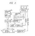
- FIG. 1 the basic construction of a measuring apparatus according to the present invention is described.
- a semiconductor specimen 1 to be measured is held on a stage 2 and its temperature is varied through contact with the stage 2 which is equipped with a heating/cooling device. It is desirable that the heating/cooling device is constructed so as to be able to change the specimen temperature from -183°C (liquid nitrogen temperature) to 475 C (the upper limit temperature below which oxygen donors are not generated in the semiconductor specimen 1 in a short period). In a simplified case, the specimen temperature may be changed from about 20 C (room temperature) to about 280 C (the upper limit temperature below which a tool made of fluorocarbon polymers (e.g., Teflon, TM of Dupont Co.) can be in practical use). In the case where the stage 2 is capable of cooling the specimen 1 to a temperature lower than the room temperature, there are required a specimen chamber and a mechanism for providing a vacuum condition or a dry gas inside the chamber.
- a tool made of fluorocarbon polymers e.g., Teflon, TM of Dupont Co.
- Minority carriers are generated in the semiconductor specimen 1, in a non-contact manner, by an energy beam emitted from a beam source 3, such as a laser diode, which is driven by a driver 4.
- a beam source 3 such as a laser diode
- a signal reflecting the recombination/extinction process of minority carriers is detected, also in a non-contact manner, by a probe 5 such as a combination of a microwave oscillator and a microwave detector.
- a controller 6 controls the temperature of the specimen 1, and also controls the energy beam emission of the beam source 3 and the signal detection of the probe 5/measuring means 7 so that these operations are performed in a synchronized manner. Based on an output signal from the probe 5, the measuring means 7 provides a signal decay curve, which is then stored by a memory means 8.
- the signal decay curves are sequentially obtained at a plurality of specimen temperatures in an arbitrarily determined range, and then stored in the memory means 8.
- conditions other than the specimen temperature such as those related to the minority carrier generation and a measurement position of the specimen 1, are kept unchanged.
- the signal-sampling condition may be selected arbitrarily as long as it does not affect the analyzing process described below.
- a deep energy level of a particular impurity is determined, in a computing means 9, by subjecting the signal decay curves to the following analyzing procedure.
- a difference between signal values at times ti and t 2 is calculated as: where optionally determined times t i and t 2 are measured from the start of the minority carrier generation, i.e., excitation of the specimen 1.
- a specimen temperature T m at which the above AS(T) takes the maximum and a value w defined by:
- the above analyzing procedure is the same as that of the capacitance DLTS method, which was established by D. V. Lang, except that the invention utilizes the original signals reflecting the recombination/extinction process of minority carriers while the conventional DLTS method analyzes the signals representing the emission/generation process of minority carriers from deep impurity levels in a depletion layer.
- the computing procedure is the same between the two methods, the difference of the signals to be analyzed is essential and mechanism of the analysis is totally different.
- FIG. 2 is a block diagram showing a measuring system used in this experiment.
- a specimen-holding stage 12 consists of a quartz plate 12a which is in contact with a silicon wafer 11, and a heater 12b which can change the temperature of the wafer 11 from the room temperature to 250 C. Insertion of the quartz plate 12a is to electrically isolate the wafer 11 from the heater 12b and to maintain the purity of the wafer 11.
- the wafer 11 is irradiated with a laser beam having a wavelength of 910 nm emitted from a laser diode 13 which is driven by a pulse generator 14.
- An output detection voltage signal of the microwave detector 15d is provided to an oscilloscope 17, in which the voltage signal is displayed and sampled/digitized.
- the resultant data are finally sent to a computer 16 as signal decay curve data.
- the computer 16 stores the decay curve data and performs the computing procedure described above. Measurement results are displayed on a CRT display 21.
- the computer 16 sends a control signal to a temperature controller 20 to thereby control the heater 12b, as well as to the oscillator driver 15b to thereby control the Gunn oscillator 15a. Further, the computer 16 sends a trigger to the pulse generator 14 and oscillscope 17 so that the emission of the excitation laser beam and the signal detecting operation are carried out in a synchronized manner.
- Each unit of the measuring system was adjusted preliminarily so that the response of the microwave impedance coupling became approximately linear. Further, the output power of the laser diode 13 was adjusted so that the peak value of the output signal from the microwave detector 15d fell within the range of from 500 mV to 1500 mV. After completion of these adjustments, measurements were conducted to obtain the signal decay curves while changing the specimen temperature from 50 C to 206 C with a step of 4 C. It is noted here that this sampling condition of the specimen temperature was just selected so as to satisfy the system's memory capacity for the decay curves, and it is desirable, to achive more reliable measurements, to employ as broad a temperature range and as small a step as possible.
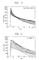
- Figs. 3 and 4 show examples of the output decay curve data obtained from a non-metal-doped Si wafer and a Ni-doped Si wafer, respectively. Each figure contains decay curves obtained at a plurality of specimen temperatures, and each decay curve corresponds to one temperature.
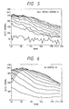
- Figs. 5 and 6 are graphs showing examples of the relationship between the difference of the output data at ti and t 2 (DLTS signal) and the specimen temperature for the non-metal-doped Si wafer and the Ni-doped Si wafer, respectively.
- Fig. 7 shows examples of the plot of In(w/T m 2 ) vs 1,000/T m for various impurity metals, which were obtained by the experimental measurements.
- the activation energy of each deep impurity level was determined from the slope of the line corresponding to the impurity level.
- This experiment shows that the invention makes it possible to measure a deep impurity level in a non-destructive manner without subjecting a specimen to any special treatment and also without any physical contact to the mirror-polished side of a specimen, which contact would affect the succeeding manufacture of a semiconductor device.
- the invention is fundamental to generate minority carriers in a non-contact manner, obtain, also in a non-contact manner, the signals reflecting the recombination/extinction process of minority carriers for a plurality of specimen temperatures, and perform the above analysis with respect to the signals thus obtained.
- the excitation of a semiconductor specimen to generate minority carriers can be performed with any electromagnetic wave having an energy higher than the bandgap of the semiconductor specimen, which is about 0.66 eV in the case of Ge and about 1.1 eV in the case of Si. Therefore, the invention does not impose any limitation on the type of the excitation electromagnetic wave except for its energy. Minority carriers may be directly injected by irradiating a specimen with an electron beam, positron beam, charged particle beam, or the like. However, in practice the use of such beams requires a specimen to be placed in vacuum, which deteriorates economy and operational easiness of the measuring apparatus.
- the wavelength should be within the range defined by the wavelengths corresponding to the bandgap energy of Si and about 2.5 eV.
- a signal reflecting the recombination process of minority carriers may be picked up in a non-contact manner by detecting the change in dielectric constant of a specimen. Therefore, in addition to the method utilizing the microwave impedance coupling as described in the above example, a usable signal may be obtained by other methods such as the detection of induction current based on the Faraday's law and the measurement of reflectance or transmittance of an electromagnetic wave.
- the probe 3 consists of an induction coil, an a.c. oscillator and a power meter.
- the operational principle of the invention requires the specimen-holding stage 2 to control the specimen temperature, the methods other than the impedance coupling method and reflectance measurement using an electromagnetic wave, including a microwave, are not suitable. This is because, with such other methods, the stage 2 necessarily becomes complicated, deteriorating economy and operational easiness of the measuring apparatus.
- the above description is devoted to the case in which only one impurity energy level is measured for a single specimen.
- the present invention is applicable to the case of measuring a plurality of impurity levels included in a single specimen. In this latter case, although it suffices to obtain the signals one time, the analyzing process should be conducted at a plurality of times corresponding to the number of impurity levels to be measured.
- the present invention has realized the non-contact, non-destructive measurement of a deep impurity level in a semiconductor substrate by improving and extending the measuring system and signal processing system of the non-contact measuring method of the monority carrier lifetime, and further applying the data analyzing procedure of the DLTS method which in itself belongs to a different category.
- it has become possible to easily determine an impurity level existing in a specimen itself in a short period of time without receiving any adverse influence from a process of forming an electrode on a specimen, and further to use, as an actual substrate for a semiconductor device, the specimen itself which has been subjected to the measurement.
- the invention does not necessarily require the cooling of a specimen by liquid nitrogen etc., there are only few limitations on the shape of a specimen and the structure of the specimen-holding part. This presents the simplification of the apparatus structure and a resultant improvement in economy, and also facilitates the application to the mapping measurement which could not be attained by the prior art without constructing an extremely complicated apparatus.
- the invention since, unlike the conventional DLTS method, the invention does not require the formation of a depletion layer in a semiconductor specimen, it may provide a possibility of identifying an impurity level which cannot be determined by the conventional DLTS method.
Landscapes
- Physics & Mathematics (AREA)
- Health & Medical Sciences (AREA)
- Electromagnetism (AREA)
- Toxicology (AREA)
- General Physics & Mathematics (AREA)
- Testing Or Measuring Of Semiconductors Or The Like (AREA)
Applications Claiming Priority (2)
| Application Number | Priority Date | Filing Date | Title |
|---|---|---|---|
| JP2211122A JP2702807B2 (ja) | 1990-08-09 | 1990-08-09 | 半導体中の深い不純物準位の測定方法及びその装置 |
| JP211122/90 | 1990-08-09 |
Publications (2)
| Publication Number | Publication Date |
|---|---|
| EP0470692A2 true EP0470692A2 (en) | 1992-02-12 |
| EP0470692A3 EP0470692A3 (OSRAM) | 1994-02-23 |
Family
ID=16600762
Family Applications (1)
| Application Number | Title | Priority Date | Filing Date |
|---|---|---|---|
| EP91304408A Withdrawn EP0470692A2 (en) | 1990-08-09 | 1991-05-16 | Method and apparatus for measuring a deep inpurity level of a semiconductor crystal |
Country Status (3)
| Country | Link |
|---|---|
| US (1) | US5047713A (OSRAM) |
| EP (1) | EP0470692A2 (OSRAM) |
| JP (1) | JP2702807B2 (OSRAM) |
Cited By (2)
| Publication number | Priority date | Publication date | Assignee | Title |
|---|---|---|---|---|
| WO2001061745A3 (en) * | 2000-02-17 | 2002-01-31 | Semilab Felvezeto Fiz Lab Rt | Surface passivation method and arrangement for measuring the lifetime of minority carriers in semiconductors |
| RU2431216C1 (ru) * | 2010-06-15 | 2011-10-10 | Государственное образовательное учреждение высшего профессионального образования Рязанский государственный радиотехнический университет | Способ определения энергии ионизации глубоких уровней в полупроводниковых барьерных структурах и устройство для его осуществления |
Families Citing this family (28)
| Publication number | Priority date | Publication date | Assignee | Title |
|---|---|---|---|---|
| US5646540A (en) * | 1989-04-19 | 1997-07-08 | Interuniversitair Micro-Elektronic Centrum Vzw | Apparatus and method for measuring electromagnetic ageing parameter of a circuit element and predicting its values |
| US5406214A (en) * | 1990-12-17 | 1995-04-11 | Semilab Felvezeto Fizikai Lab, Rt | Method and apparatus for measuring minority carrier lifetime in semiconductor materials |
| JP2943474B2 (ja) * | 1992-01-20 | 1999-08-30 | 日本電気株式会社 | 波形解析方法 |
| US5361032A (en) * | 1992-01-27 | 1994-11-01 | Motorola, Inc. | Method of troubleshooting electronic circuit board assemblies using temperature isolation |
| JPH06151538A (ja) * | 1992-02-03 | 1994-05-31 | Leo Giken:Kk | 半導体ウエハの評価方法及びその装置 |
| US5417494A (en) * | 1992-05-01 | 1995-05-23 | Exid, Inc. | Contactless testing of electronic materials and devices using microwaves |
| JPH0697248A (ja) * | 1992-09-16 | 1994-04-08 | Shin Etsu Handotai Co Ltd | ライフタイム測定装置及びこれを用いた測定方法 |
| JPH07105427B2 (ja) * | 1992-10-19 | 1995-11-13 | 学校法人幾徳学園 | 半導体材料のライフタイム評価方法とその装置 |
| US5521839A (en) * | 1993-09-02 | 1996-05-28 | Georgia Tech Research Corporation | Deep level transient spectroscopy (DLTS) system and method |
| JPH07153809A (ja) * | 1993-11-26 | 1995-06-16 | Nec Corp | 半導体基板の不純物分析装置および不純物分析方法 |
| CA2126481C (en) * | 1994-06-22 | 2001-03-27 | Andreas Mandelis | Non-contact photothermal method for measuring thermal diffusivity and electronic defect properties of solids |
| JP3670051B2 (ja) * | 1995-06-06 | 2005-07-13 | 株式会社神戸製鋼所 | 半導体試料のキャリアのライフタイム測定方法及びその装置 |
| US5847573A (en) * | 1995-10-13 | 1998-12-08 | Massachusetts Technological Laboratory, Inc. | Method and apparatus for structure characterization of layered semiconductors |
| US5966019A (en) * | 1996-04-24 | 1999-10-12 | Boxer Cross, Inc. | System and method for measuring properties of a semiconductor substrate in a fabrication line |
| US5867034A (en) * | 1997-01-30 | 1999-02-02 | Sokolov; Vladimir | Non-destructive method and apparatus for monitoring carrier lifetime of a semiconductor sample during fabrication |
| TW359864B (en) * | 1997-03-13 | 1999-06-01 | United Microelectronics Corp | Method for detecting dosage of polysilicon implantation |
| US5929652A (en) * | 1997-09-02 | 1999-07-27 | Midwest Research Institute | Apparatus for measuring minority carrier lifetimes in semiconductor materials |
| US6369603B1 (en) * | 1997-09-02 | 2002-04-09 | Midwest Research Institute | Radio frequency coupling apparatus and method for measuring minority carrier lifetimes in semiconductor materials |
| US6275060B1 (en) * | 1997-09-02 | 2001-08-14 | Midwest Research Institute | Apparatus and method for measuring minority carrier lifetimes in semiconductor materials |
| US6078183A (en) | 1998-03-03 | 2000-06-20 | Sandia Corporation | Thermally-induced voltage alteration for integrated circuit analysis |
| US6260998B1 (en) * | 2000-01-19 | 2001-07-17 | Visteon Global Technologies, Inc. | Method for specifying accelerated thermal cycling tests for electronic solder joint durability |
| US6909273B1 (en) * | 2000-05-05 | 2005-06-21 | Chartered Semiconductor Manufacturing Ltd. | Zero-temperature-gradient zero-bias thermally stimulated current technique to characterize defects in semiconductors or insulators |
| US6549022B1 (en) * | 2000-06-02 | 2003-04-15 | Sandia Corporation | Apparatus and method for analyzing functional failures in integrated circuits |
| TWI223097B (en) * | 2003-04-14 | 2004-11-01 | Toppoly Optoelectronics Corp | Method and apparatus for testing OLED pixels |
| US7520667B2 (en) * | 2006-05-11 | 2009-04-21 | John Bean Technologies Ab | Method and system for determining process parameters |
| ATE514095T1 (de) * | 2007-09-11 | 2011-07-15 | Soitec Silicon On Insulator | Volumenlebensdauermessung |
| US7898280B2 (en) * | 2008-09-08 | 2011-03-01 | Emil Kamieniecki | Electrical characterization of semiconductor materials |
| CN112786472B (zh) * | 2021-01-06 | 2023-01-10 | 电子科技大学 | 一种介电温度系数修正的深能级瞬态谱测试方法 |
Family Cites Families (12)
| Publication number | Priority date | Publication date | Assignee | Title |
|---|---|---|---|---|
| DE1644032A1 (de) * | 1966-12-30 | 1971-03-25 | Texas Instruments Inc | Verfahren zur Einstellung der Fremdatomkonzentration bei Halbleitern |
| US3605015A (en) * | 1970-01-19 | 1971-09-14 | Bell Telephone Labor Inc | Method and apparatus for determining deep impurity concentration in semiconductors |
| HU181136B (en) * | 1980-06-07 | 1983-06-28 | Mta Mueszaki Fiz Kutato Inteze | Method and instrument for measuring change in transient capacity of semiconducting elements |
| US4427937A (en) * | 1981-09-25 | 1984-01-24 | Lin Hung C | Method of measuring time constant using a spectrum analyzer |
| US4551674A (en) * | 1982-11-12 | 1985-11-05 | At&T Bell Laboratories | Noncontacting conductivity type determination and surface state spectroscopy of semiconductor materials |
| JPS59141238A (ja) * | 1983-02-01 | 1984-08-13 | Hitachi Ltd | キヤリア寿命測定装置 |
| DE3407850A1 (de) * | 1984-02-29 | 1985-09-05 | Hahn-Meitner-Institut für Kernforschung Berlin GmbH, 1000 Berlin | Mikrowellen-messverfahren und -messapparatur zur kontaktlosen und zerstoerungsfreien untersuchung photoempfindlicher materialien |
| JPS61101045A (ja) * | 1984-10-24 | 1986-05-19 | Hitachi Ltd | 半導体評価方法 |
| US4755748A (en) * | 1985-06-05 | 1988-07-05 | Bell Communications Research, Inc. | Method and apparatus for analyzing semiconductor devices using charge-sensitive electron-beam-injected-carrier microscopy |
| HU196262B (en) * | 1986-03-17 | 1988-10-28 | Mta Mueszaki Fiz Kutato Inteze | Method for testing electrically active impuritles in semiconductor materials and structures and measuring arrangement for implementing method |
| US4875004A (en) * | 1988-06-01 | 1989-10-17 | The United States Of America As Represented By The Secretary Of The Army | High speed semiconductor characterization technique |
| JPH067564B2 (ja) * | 1988-09-07 | 1994-01-26 | 三菱マテリアル株式会社 | ウェーハ表面の半導体特性測定方法 |
-
1990
- 1990-08-09 JP JP2211122A patent/JP2702807B2/ja not_active Expired - Lifetime
- 1990-11-14 US US07/612,926 patent/US5047713A/en not_active Expired - Fee Related
-
1991
- 1991-05-16 EP EP91304408A patent/EP0470692A2/en not_active Withdrawn
Cited By (3)
| Publication number | Priority date | Publication date | Assignee | Title |
|---|---|---|---|---|
| WO2001061745A3 (en) * | 2000-02-17 | 2002-01-31 | Semilab Felvezeto Fiz Lab Rt | Surface passivation method and arrangement for measuring the lifetime of minority carriers in semiconductors |
| US6653850B2 (en) | 2000-02-17 | 2003-11-25 | Semilab Felvezto Fizikai Laboratorium Rt | Surface passivation method and arrangement for measuring the lifetime of minority carriers in semiconductors |
| RU2431216C1 (ru) * | 2010-06-15 | 2011-10-10 | Государственное образовательное учреждение высшего профессионального образования Рязанский государственный радиотехнический университет | Способ определения энергии ионизации глубоких уровней в полупроводниковых барьерных структурах и устройство для его осуществления |
Also Published As
| Publication number | Publication date |
|---|---|
| JP2702807B2 (ja) | 1998-01-26 |
| EP0470692A3 (OSRAM) | 1994-02-23 |
| US5047713A (en) | 1991-09-10 |
| JPH0493043A (ja) | 1992-03-25 |
Similar Documents
| Publication | Publication Date | Title |
|---|---|---|
| US5047713A (en) | Method and apparatus for measuring a deep impurity level of a semiconductor crystal | |
| US5907764A (en) | In-line detection and assessment of net charge in PECVD silicon dioxide (oxide) layers | |
| Lightowlers et al. | Determination of boron in natural semiconducting diamond by prompt particle nuclear microanalysis and Schottky barrier differential-capacitance measurements | |
| US4259574A (en) | Microanalysis by pulse laser emission spectroscopy | |
| EP0545523B1 (en) | Method for evaluation of spatial distribution of deep level concentration in semiconductor crystal | |
| JPH0587140B2 (OSRAM) | ||
| Huebener | Scanning electron microscopy at very low temperatures | |
| US6653850B2 (en) | Surface passivation method and arrangement for measuring the lifetime of minority carriers in semiconductors | |
| Balk | Scanning electron acoustic microscopy | |
| Koropecki et al. | Density of states in the gap of amorphous semiconductors determined from modulated photocurrent measurements in the recombination regime | |
| EP0511145B1 (en) | Method for determining the thickness of an interfacial polysilicon/silicon oxide film | |
| Jakubowicz | On the theory of electron‐beam‐induced current contrast from pointlike defects in semiconductors | |
| US4569728A (en) | Selective anodic oxidation of semiconductors for pattern generation | |
| Marchishin | Deep level profiling using an admittance spectroscopy method | |
| KR100319676B1 (ko) | 시료전류 스펙트로스코피 표면측정을 위한 방법 및 장치 | |
| Eränen et al. | Simultaneous measurement of recombination lifetime and surface recombination velocity | |
| Benton | Characterization of defects in semiconductors by deep level transient spectroscopy | |
| US5760594A (en) | Contamination monitoring using capacitance measurements on MOS structures | |
| Ahrenkiel et al. | Injection level lifetime spectroscopy of impurities in semiconductors | |
| US6914442B2 (en) | Method for measuring resistivity of semiconductor wafer | |
| JPS61101045A (ja) | 半導体評価方法 | |
| JPS6253944B2 (OSRAM) | ||
| HUP9902355A2 (hu) | Nagy érzékenységű eljárás és berendezés kisebbségi töltéshordozók élettartamának mérésére félvezető anyagokban | |
| Heydenreich et al. | Characterization of defects in semiconductors by combined application of SEM (EBIC) and SDLTS | |
| SU1581138A1 (ru) | Способ определени времени релаксации неравновесных возбуждений |
Legal Events
| Date | Code | Title | Description |
|---|---|---|---|
| PUAI | Public reference made under article 153(3) epc to a published international application that has entered the european phase |
Free format text: ORIGINAL CODE: 0009012 |
|
| AK | Designated contracting states |
Kind code of ref document: A2 Designated state(s): DE FR GB |
|
| PUAL | Search report despatched |
Free format text: ORIGINAL CODE: 0009013 |
|
| AK | Designated contracting states |
Kind code of ref document: A3 Designated state(s): DE FR GB |
|
| 17P | Request for examination filed |
Effective date: 19940621 |
|
| 17Q | First examination report despatched |
Effective date: 19950816 |
|
| STAA | Information on the status of an ep patent application or granted ep patent |
Free format text: STATUS: THE APPLICATION IS DEEMED TO BE WITHDRAWN |
|
| 18D | Application deemed to be withdrawn |
Effective date: 19951228 |