EP0468210A2 - Schaltung zum Ansteuern einer treibenden Schaltung infolge eines digitalen Signals - Google Patents
Schaltung zum Ansteuern einer treibenden Schaltung infolge eines digitalen Signals Download PDFInfo
- Publication number
- EP0468210A2 EP0468210A2 EP91110383A EP91110383A EP0468210A2 EP 0468210 A2 EP0468210 A2 EP 0468210A2 EP 91110383 A EP91110383 A EP 91110383A EP 91110383 A EP91110383 A EP 91110383A EP 0468210 A2 EP0468210 A2 EP 0468210A2
- Authority
- EP
- European Patent Office
- Prior art keywords
- transistor
- source
- transistors
- drain
- gate
- Prior art date
- Legal status (The legal status is an assumption and is not a legal conclusion. Google has not performed a legal analysis and makes no representation as to the accuracy of the status listed.)
- Granted
Links
Images
Classifications
-
- H—ELECTRICITY
- H04—ELECTRIC COMMUNICATION TECHNIQUE
- H04L—TRANSMISSION OF DIGITAL INFORMATION, e.g. TELEGRAPHIC COMMUNICATION
- H04L25/00—Baseband systems
- H04L25/02—Details ; arrangements for supplying electrical power along data transmission lines
- H04L25/03—Shaping networks in transmitter or receiver, e.g. adaptive shaping networks
-
- H—ELECTRICITY
- H03—ELECTRONIC CIRCUITRY
- H03K—PULSE TECHNIQUE
- H03K3/00—Circuits for generating electric pulses; Monostable, bistable or multistable circuits
- H03K3/02—Generators characterised by the type of circuit or by the means used for producing pulses
- H03K3/353—Generators characterised by the type of circuit or by the means used for producing pulses by the use, as active elements, of field-effect transistors with internal or external positive feedback
- H03K3/356—Bistable circuits
- H03K3/356104—Bistable circuits using complementary field-effect transistors
- H03K3/356113—Bistable circuits using complementary field-effect transistors using additional transistors in the input circuit
- H03K3/35613—Bistable circuits using complementary field-effect transistors using additional transistors in the input circuit the input circuit having a differential configuration
-
- H—ELECTRICITY
- H03—ELECTRONIC CIRCUITRY
- H03K—PULSE TECHNIQUE
- H03K3/00—Circuits for generating electric pulses; Monostable, bistable or multistable circuits
- H03K3/02—Generators characterised by the type of circuit or by the means used for producing pulses
- H03K3/353—Generators characterised by the type of circuit or by the means used for producing pulses by the use, as active elements, of field-effect transistors with internal or external positive feedback
- H03K3/356—Bistable circuits
- H03K3/356017—Bistable circuits using additional transistors in the input circuit
- H03K3/356034—Bistable circuits using additional transistors in the input circuit the input circuit having a differential configuration
Definitions
- the present invention relates to a driving circuit for driving a floating circuit in response to a digital signal.
- the invention relates to such a driving circuit which is suitable for implementation in integrated circuit form with BCD technology.
- the devices used to drive a floating circuit with a digital or logic signal also known as level shifters, must not lose the logic signal in the variations caused by the charging and discharging of the parasitic input capacitor of the floating circuit while the voltage thereof shifts with respect to the ground.
- the parasitic capacitor In order that the input node of the floating circuit may assuredly follow the variations of the driving signal which drives the level shifter, the parasitic capacitor must in fact charge and discharge with the same speed as the driving logic signal, and for this purpose the input node of the floating circuit must be connected to a low-impedance point.
- a simple way of solving the problem consists in causing a current to flow in a resistor which has one terminal at the high floating voltage and the opposite terminal connected to the input of the floating circuit.
- the resistor must have a small value, for example 1 kohm, and the voltage drop required across the resistor in order to produce a logic signal on the floating circuit requires a high current and thus a considerable power absorption.
- a solution consists in providing a flip-flop at the input of the floating circuit, with a double pulse drive in two high-value resistors for switching the flip-flop.
- current consumption in steady-state conditions is low, but in order to maintain a low impedance even during switching it is necessary to provide current sources for rapidly charging the parasitic capacitor.
- This entails a certain circuital complexity, besides the fact that in any case the presence of the flip-flop entails the risk of errors on the phases of the logic signal in case of outside noise during rise and fall.
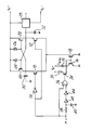
- a driving circuit for driving a floating circuit in response to a digital signal comprising a digital signal source which produces said digital signal; first, second, third and fourth transistors; a current source; and a voltage source; each of said first and second transistors being a DMOS transistor having a source, a drain and a gate; each of said third and fourth transistors being a MOS transistor having a source, a drain and a gate; said first and third transistors being connected in series between said current source and said voltage source; said second and fourth transistors being connected in series between said current source and said voltage source; said first and second transistors being driven in opposite phase on their respective gates starting from said digital signal; the gate of said third transistor being connected to the connection of said fourth transistor to said second transistor; the gate of said fourth transistor being connected to the connection of said third transistor to said first transistor; and the driving output of said driving circuit being the connection of said second transistor to said fourth transistor.
- the third and fourth transistors are P-channel transistors
- the DMOS transistors are common-source connected with the sources of the two DMOS transistors being biased by the current source
- the drains of the DMOS transistors are connected to respective drains of respective P-channel transistors.
- Each of the P-channel transistors has its source connected to a high voltage source and its gate connected to the drain of the other P-channel transistor. Zener diodes can be employed to limit the voltage drop between the source and gate of each P-channel transistor.
- the current source can comprise the combination of a circuit for providing a reference current and a circuit for providing a short pulse in response to the leading portion of a digital signal pulse.
- the short pulse can be produced by an XOR (exclusive OR) circuit having the digital signal and a delayed version of the digital signal as inputs thereto.
- two DMOS transistors 10, 12 are driven in opposite phase by a digital input signal source IN by passing the digital input signal directly from source IN to the gate of DMOS transistor 12 and by passing the digital input signal through an inverter 14 to the gate of the DMOS transistor 10.
- the sources of the two DMOS transistors are connected to a current mirror which provides a biasing current.
- the current mirror comprises transistors 16, 18 having their gates connected to each other and to the drain of transistor 16.
- the sources of transistors 16 and 18 are connected to a reference voltage, e.g. ground.
- the drain of transistor 18 is connected to the source of each of DMOS transistors 10 and 12, while a reference current source 19 is connected between a high voltage source and the drain of transistor 16.
- Reference current source 19 provides a reference current I BIAS .
- the loads on the drains of the two DMOS transistors 10, 12 are constituted by P-channel transistors 20, 22, with the transistors 10 and 20 being connected in series with each other between the current source and a high voltage source V F I and the transistor 12 and 22 being similarly connected in series with each other between the current source and the high voltage source.
- the gate of transistor 20 is driven by the drain of transistor 22, and the gate of transistor 22 is driven by the drain of transistor 20.
- Zener diode 24 is connected between the gate and source of transistor 20, while Zener diode 26 is connected between the gate and source of transistor 22, to limit the voltage drop between the source and the gate of the respective P-channel transistor.
- the drain of the DMOS transistor 12 is connected to the drive input of a per se known floating circuit 28 powered by the floating voltages Vp + , V F -.
- the P-channel transistors 20, 22 are dimensioned so as to be able to rapidly charge the parasitic capacitors indicated by 30, 32, i.e. so as to have a low output resistance, for example approximately 1 kohm.
- the current flowing through the "on" DMOS transistor, which is normally equal to I BIAS can be relatively small, for example approximately 280 uA.
- the driving circuit furthermore preferably comprises an auxiliary circuit for generating an additional short duration, high current pulse during the switching operation.
- the auxiliary circuit comprises a transistor 34 which is source-follower connected to the drain of transistor 16.
- a resistor 35 is connected between the drain of transistor 34 and voltage source Vp + .
- the transistor 34 is driven by an XOR circuit 36, which receives the digital signal from digital signal source IN on one input and receives the same signal, delayed by a delay chain on its other input.
- the delay chain can be formed by a series resistor 38, a parallel capacitor 40 and two cascade inverters 42, 44 connected between the source IN and the other input of the XOR. It can thus be seen that the source follower 34 is driven by a short pulse from the XOR which appears during the period between the arrival at one input of XOR 36 of the leading edge of the digital pulse from digital signal source IN and the arrival at the other input of XOR 36 of the delayed version of the leading edge of the digital pulse.
- the characteristics of the delay chain can be selected to provide a pulse at the output of XOR 36 which is shorter in duration than the digital input pulse from digital signal source IN.
- this auxiliary circuit injects a current pulse in parallel to the reference I BIAS .
- the added pulse from the auxiliary circuit can have a high value, for example 10 mA, without significantly affecting the average absorption of the driving circuit as a whole.
Landscapes
- Engineering & Computer Science (AREA)
- Power Engineering (AREA)
- Computer Networks & Wireless Communication (AREA)
- Signal Processing (AREA)
- Electronic Switches (AREA)
- Logic Circuits (AREA)
- Transmission And Conversion Of Sensor Element Output (AREA)
- Eye Examination Apparatus (AREA)
Applications Claiming Priority (2)
| Application Number | Priority Date | Filing Date | Title |
|---|---|---|---|
| IT02108790A IT1243692B (it) | 1990-07-27 | 1990-07-27 | Dospositivo per il pilotaggio di un circuito flottante con un segnale digitale |
| IT2108790 | 1990-07-27 |
Publications (3)
| Publication Number | Publication Date |
|---|---|
| EP0468210A2 true EP0468210A2 (de) | 1992-01-29 |
| EP0468210A3 EP0468210A3 (en) | 1992-04-22 |
| EP0468210B1 EP0468210B1 (de) | 1999-08-18 |
Family
ID=11176537
Family Applications (1)
| Application Number | Title | Priority Date | Filing Date |
|---|---|---|---|
| EP91110383A Expired - Lifetime EP0468210B1 (de) | 1990-07-27 | 1991-06-24 | Schaltung zum Ansteuern einer schwebenden Schaltung mit einem digitalen Signal |
Country Status (6)
| Country | Link |
|---|---|
| US (1) | US5146109A (de) |
| EP (1) | EP0468210B1 (de) |
| JP (1) | JPH04270513A (de) |
| KR (1) | KR920003704A (de) |
| DE (1) | DE69131532T2 (de) |
| IT (1) | IT1243692B (de) |
Families Citing this family (7)
| Publication number | Priority date | Publication date | Assignee | Title |
|---|---|---|---|---|
| GB9320246D0 (en) * | 1993-10-01 | 1993-11-17 | Sgs Thomson Microelectronics | A driver circuit |
| DE69319910T2 (de) * | 1993-10-29 | 1998-12-10 | Sgs-Thomson Microelectronics S.R.L., Agrate Brianza, Mailand/Milano | Eingangs-/Ausgangsschnittstellenschaltung für analoge und digitale Signale |
| JP3705880B2 (ja) * | 1996-11-28 | 2005-10-12 | 富士通株式会社 | レベルコンバータ及び半導体装置 |
| US6777992B2 (en) * | 2002-04-04 | 2004-08-17 | The Regents Of The University Of Michigan | Low-power CMOS flip-flop |
| US7622977B2 (en) * | 2005-10-27 | 2009-11-24 | The Regents Of The University Of Michigan | Ramped clock digital storage control |
| US7973565B2 (en) * | 2007-05-23 | 2011-07-05 | Cyclos Semiconductor, Inc. | Resonant clock and interconnect architecture for digital devices with multiple clock networks |
| WO2011046979A2 (en) * | 2009-10-12 | 2011-04-21 | Cyclos Semiconductor, Inc. | Method for selecting natural frequency in resonant clock distribution networks with no inductor overhead |
Family Cites Families (8)
| Publication number | Priority date | Publication date | Assignee | Title |
|---|---|---|---|---|
| US4521703A (en) * | 1982-08-30 | 1985-06-04 | Rca Corporation | High speed sense amplifier |
| US4532436A (en) * | 1983-09-30 | 1985-07-30 | Rca Corporation | Fast switching circuit |
| US4695744A (en) * | 1985-12-16 | 1987-09-22 | Rca Corporation | Level shift circuit including source follower output |
| US4845381A (en) * | 1987-10-01 | 1989-07-04 | Vlsi Technology, Inc. | Voltage level shifting circuit |
| US4795917A (en) * | 1987-11-02 | 1989-01-03 | Pacific Bell | Low power high voltage driver circuit |
| IT1221251B (it) * | 1988-02-25 | 1990-06-27 | Sgs Thomson Microelectronics | Circuito mos per il pilotaggio di un carico dal lato alto della alimentazione |
| JPH07105448B2 (ja) * | 1988-03-14 | 1995-11-13 | 日本電気株式会社 | Mos型集積回路 |
| JPH0727717B2 (ja) * | 1988-07-13 | 1995-03-29 | 株式会社東芝 | センス回路 |
-
1990
- 1990-07-27 IT IT02108790A patent/IT1243692B/it active IP Right Grant
-
1991
- 1991-06-24 DE DE69131532T patent/DE69131532T2/de not_active Expired - Lifetime
- 1991-06-24 EP EP91110383A patent/EP0468210B1/de not_active Expired - Lifetime
- 1991-07-23 JP JP3182419A patent/JPH04270513A/ja active Pending
- 1991-07-24 KR KR1019910012664A patent/KR920003704A/ko not_active Withdrawn
- 1991-07-25 US US07/736,003 patent/US5146109A/en not_active Expired - Lifetime
Also Published As
| Publication number | Publication date |
|---|---|
| IT9021087A1 (it) | 1992-01-27 |
| IT1243692B (it) | 1994-06-21 |
| KR920003704A (ko) | 1992-02-29 |
| US5146109A (en) | 1992-09-08 |
| DE69131532D1 (de) | 1999-09-23 |
| DE69131532T2 (de) | 2000-04-06 |
| JPH04270513A (ja) | 1992-09-25 |
| EP0468210A3 (en) | 1992-04-22 |
| EP0468210B1 (de) | 1999-08-18 |
| IT9021087A0 (it) | 1990-07-27 |
Similar Documents
| Publication | Publication Date | Title |
|---|---|---|
| US5723986A (en) | Level shifting circuit | |
| US6646469B2 (en) | High voltage level shifter via capacitors | |
| US6624672B2 (en) | Output buffer with constant switching current | |
| KR920010819B1 (ko) | 레벨 변환 기능을 갖는 출력버퍼회로 | |
| KR20000017655A (ko) | 링 발진기 및 지연 회로 | |
| EP0086090A1 (de) | Treiberschaltung für kapazitive Lasten | |
| KR960039641A (ko) | 고내압회로 및 전압레벨 변환회로 | |
| JPH0757474A (ja) | 半導体メモリ装置のチップ初期化信号発生回路 | |
| KR900001042A (ko) | Cmos 인버터를 구비한 반도체 집적회로 | |
| JP2748950B2 (ja) | パワーオンリセット回路 | |
| KR910015114A (ko) | 반도체 디지탈 회로 | |
| EP0351820B1 (de) | Ausgangschaltung | |
| US11522446B2 (en) | Low input supply and low output impedance charge pump circuit configured for positive and negative voltage generation | |
| JPH01288010A (ja) | ドライバ回路 | |
| KR950007287A (ko) | 디지탈 신호 처리용 지연 회로 | |
| EP0468210A2 (de) | Schaltung zum Ansteuern einer treibenden Schaltung infolge eines digitalen Signals | |
| US7816969B2 (en) | Level shifter circuit | |
| US4472645A (en) | Clock circuit for generating non-overlapping pulses | |
| US4352996A (en) | IGFET Clock generator circuit employing MOS boatstrap capacitive drive | |
| JPS61222318A (ja) | パワ−オンリセツト回路 | |
| JP3261151B2 (ja) | リセット信号発生回路装置 | |
| KR910002083A (ko) | 출력회로 | |
| JP2585128Y2 (ja) | 半導体集積回路 | |
| JP2541289B2 (ja) | 出力回路 | |
| JP2891832B2 (ja) | Lcdドライバー回路 |
Legal Events
| Date | Code | Title | Description |
|---|---|---|---|
| PUAI | Public reference made under article 153(3) epc to a published international application that has entered the european phase |
Free format text: ORIGINAL CODE: 0009012 |
|
| AK | Designated contracting states |
Kind code of ref document: A2 Designated state(s): DE FR GB NL SE |
|
| PUAL | Search report despatched |
Free format text: ORIGINAL CODE: 0009013 |
|
| AK | Designated contracting states |
Kind code of ref document: A3 Designated state(s): DE FR GB NL SE |
|
| 17P | Request for examination filed |
Effective date: 19920922 |
|
| 17Q | First examination report despatched |
Effective date: 19951227 |
|
| RAP3 | Party data changed (applicant data changed or rights of an application transferred) |
Owner name: STMICROELECTRONICS S.R.L. |
|
| GRAG | Despatch of communication of intention to grant |
Free format text: ORIGINAL CODE: EPIDOS AGRA |
|
| GRAG | Despatch of communication of intention to grant |
Free format text: ORIGINAL CODE: EPIDOS AGRA |
|
| GRAH | Despatch of communication of intention to grant a patent |
Free format text: ORIGINAL CODE: EPIDOS IGRA |
|
| GRAH | Despatch of communication of intention to grant a patent |
Free format text: ORIGINAL CODE: EPIDOS IGRA |
|
| GRAA | (expected) grant |
Free format text: ORIGINAL CODE: 0009210 |
|
| AK | Designated contracting states |
Kind code of ref document: B1 Designated state(s): DE FR GB NL SE |
|
| PG25 | Lapsed in a contracting state [announced via postgrant information from national office to epo] |
Ref country code: SE Free format text: THE PATENT HAS BEEN ANNULLED BY A DECISION OF A NATIONAL AUTHORITY Effective date: 19990818 Ref country code: NL Free format text: LAPSE BECAUSE OF FAILURE TO SUBMIT A TRANSLATION OF THE DESCRIPTION OR TO PAY THE FEE WITHIN THE PRESCRIBED TIME-LIMIT Effective date: 19990818 |
|
| REF | Corresponds to: |
Ref document number: 69131532 Country of ref document: DE Date of ref document: 19990923 |
|
| ET | Fr: translation filed | ||
| NLV1 | Nl: lapsed or annulled due to failure to fulfill the requirements of art. 29p and 29m of the patents act | ||
| PLBE | No opposition filed within time limit |
Free format text: ORIGINAL CODE: 0009261 |
|
| STAA | Information on the status of an ep patent application or granted ep patent |
Free format text: STATUS: NO OPPOSITION FILED WITHIN TIME LIMIT |
|
| 26N | No opposition filed | ||
| REG | Reference to a national code |
Ref country code: GB Ref legal event code: IF02 |
|
| PGFP | Annual fee paid to national office [announced via postgrant information from national office to epo] |
Ref country code: GB Payment date: 20100527 Year of fee payment: 20 Ref country code: FR Payment date: 20100729 Year of fee payment: 20 Ref country code: DE Payment date: 20100610 Year of fee payment: 20 |
|
| REG | Reference to a national code |
Ref country code: DE Ref legal event code: R071 Ref document number: 69131532 Country of ref document: DE |
|
| REG | Reference to a national code |
Ref country code: DE Ref legal event code: R071 Ref document number: 69131532 Country of ref document: DE |
|
| REG | Reference to a national code |
Ref country code: GB Ref legal event code: PE20 Expiry date: 20110623 |
|
| PG25 | Lapsed in a contracting state [announced via postgrant information from national office to epo] |
Ref country code: GB Free format text: LAPSE BECAUSE OF EXPIRATION OF PROTECTION Effective date: 20110623 |
|
| PG25 | Lapsed in a contracting state [announced via postgrant information from national office to epo] |
Ref country code: DE Free format text: LAPSE BECAUSE OF EXPIRATION OF PROTECTION Effective date: 20110625 |