EP0464492A1 - Photomaske, die in der Photolithographie benutzt wird und ein Herstellungsverfahren derselben - Google Patents
Photomaske, die in der Photolithographie benutzt wird und ein Herstellungsverfahren derselben Download PDFInfo
- Publication number
- EP0464492A1 EP0464492A1 EP91110167A EP91110167A EP0464492A1 EP 0464492 A1 EP0464492 A1 EP 0464492A1 EP 91110167 A EP91110167 A EP 91110167A EP 91110167 A EP91110167 A EP 91110167A EP 0464492 A1 EP0464492 A1 EP 0464492A1
- Authority
- EP
- European Patent Office
- Prior art keywords
- transparent
- pattern
- photomask
- transparent substrate
- transparent layer
- Prior art date
- Legal status (The legal status is an assumption and is not a legal conclusion. Google has not performed a legal analysis and makes no representation as to the accuracy of the status listed.)
- Granted
Links
Images


Classifications
-
- G—PHYSICS
- G03—PHOTOGRAPHY; CINEMATOGRAPHY; ANALOGOUS TECHNIQUES USING WAVES OTHER THAN OPTICAL WAVES; ELECTROGRAPHY; HOLOGRAPHY
- G03F—PHOTOMECHANICAL PRODUCTION OF TEXTURED OR PATTERNED SURFACES, e.g. FOR PRINTING, FOR PROCESSING OF SEMICONDUCTOR DEVICES; MATERIALS THEREFOR; ORIGINALS THEREFOR; APPARATUS SPECIALLY ADAPTED THEREFOR
- G03F7/00—Photomechanical, e.g. photolithographic, production of textured or patterned surfaces, e.g. printing surfaces; Materials therefor, e.g. comprising photoresists; Apparatus specially adapted therefor
- G03F7/70—Microphotolithographic exposure; Apparatus therefor
- G03F7/708—Construction of apparatus, e.g. environment aspects, hygiene aspects or materials
- G03F7/7095—Materials, e.g. materials for housing, stage or other support having particular properties, e.g. weight, strength, conductivity, thermal expansion coefficient
- G03F7/70958—Optical materials or coatings, e.g. with particular transmittance, reflectance or anti-reflection properties
-
- G—PHYSICS
- G03—PHOTOGRAPHY; CINEMATOGRAPHY; ANALOGOUS TECHNIQUES USING WAVES OTHER THAN OPTICAL WAVES; ELECTROGRAPHY; HOLOGRAPHY
- G03F—PHOTOMECHANICAL PRODUCTION OF TEXTURED OR PATTERNED SURFACES, e.g. FOR PRINTING, FOR PROCESSING OF SEMICONDUCTOR DEVICES; MATERIALS THEREFOR; ORIGINALS THEREFOR; APPARATUS SPECIALLY ADAPTED THEREFOR
- G03F1/00—Originals for photomechanical production of textured or patterned surfaces, e.g., masks, photo-masks, reticles; Mask blanks or pellicles therefor; Containers specially adapted therefor; Preparation thereof
- G03F1/26—Phase shift masks [PSM]; PSM blanks; Preparation thereof
- G03F1/28—Phase shift masks [PSM]; PSM blanks; Preparation thereof with three or more diverse phases on the same PSM; Preparation thereof
-
- G—PHYSICS
- G03—PHOTOGRAPHY; CINEMATOGRAPHY; ANALOGOUS TECHNIQUES USING WAVES OTHER THAN OPTICAL WAVES; ELECTROGRAPHY; HOLOGRAPHY
- G03F—PHOTOMECHANICAL PRODUCTION OF TEXTURED OR PATTERNED SURFACES, e.g. FOR PRINTING, FOR PROCESSING OF SEMICONDUCTOR DEVICES; MATERIALS THEREFOR; ORIGINALS THEREFOR; APPARATUS SPECIALLY ADAPTED THEREFOR
- G03F1/00—Originals for photomechanical production of textured or patterned surfaces, e.g., masks, photo-masks, reticles; Mask blanks or pellicles therefor; Containers specially adapted therefor; Preparation thereof
- G03F1/26—Phase shift masks [PSM]; PSM blanks; Preparation thereof
- G03F1/34—Phase-edge PSM, e.g. chromeless PSM; Preparation thereof
-
- G—PHYSICS
- G03—PHOTOGRAPHY; CINEMATOGRAPHY; ANALOGOUS TECHNIQUES USING WAVES OTHER THAN OPTICAL WAVES; ELECTROGRAPHY; HOLOGRAPHY
- G03F—PHOTOMECHANICAL PRODUCTION OF TEXTURED OR PATTERNED SURFACES, e.g. FOR PRINTING, FOR PROCESSING OF SEMICONDUCTOR DEVICES; MATERIALS THEREFOR; ORIGINALS THEREFOR; APPARATUS SPECIALLY ADAPTED THEREFOR
- G03F7/00—Photomechanical, e.g. photolithographic, production of textured or patterned surfaces, e.g. printing surfaces; Materials therefor, e.g. comprising photoresists; Apparatus specially adapted therefor
- G03F7/70—Microphotolithographic exposure; Apparatus therefor
- G03F7/70216—Mask projection systems
- G03F7/70283—Mask effects on the imaging process
Definitions
- the present invention relates to a photomask used by photolithography, and a process for making same.
- Lithography consists of a process in which a resist is first coated, then exposed to light and developed with a developer. The fineness of the resulting patterns has been improved by the development of the material of the resist, the device and method of exposure.
- the substrate 1 is composed of two different members 4 and 5 arranged side by side, of which the members 4 are transparent or transmissive layer.
- the members 4 act as phase shifters. This example is characteristic in that the phase shifter 4 is not formed on the substrate 1.
- This type of photomask is disclosed in Japanese Laid-Open Patent Publication No. 62-92439.
- phase shifter 4 of a thin film is formed on the light-shielding pattern and a transparent area outside the light-shielding area.
- the thin layer is made of photosensitive resin. Light or electron beams are radiated on a desired area in the thin layer. It is necessary to align the exposing radiation with the edges of the light-shielding patterns. This means two times of exposure, thereby resulting in a complicated exposing procedure. In addition, the alignment must be strictly accurate, otherwise a desired phase shifter will not be attained.
- a photomask In general, a photomask must be perfect, free from any defects. However, it is difficult to detect any fault in the photomask by scanning light so as to find a scattering light or a permeating light. This detecting method is likely to be inaccurate because of an out-of-focus irradiation caused by the uneven thickness of the phase shifter due to the presence of the light-shielding layer, and because of the impermeability of light in the overlapping of the light-shielding layer over the phase shifter. In this case it is necessary to produce another phase shifter so as to remedy the defects.
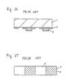
- phase shifter shown in Figure 27 the phase shifters are arranged at equal intervals. In order to achieve a desired phase difference, it is necessary to fabricate the intervals to a high precision, thereby resulting in a difficult fabrication of photomasks. Irregular intervals cannot produce fine, intricate patterns suitable for IDs used in LSls.
- the photomask of this invention which overcomes the above-discussed and numerous other disadvantages and deficiencies of the prior art, comprises a transparent substrate, and a transparent layer pattern formed on the transparent substrate, the transparent layer pattern giving a phase difference to an incident light.
- the photomask comprises a transparent substrate, and a transparent layer pattern formed on the transparent substrate, the transparent layer pattern giving a phase difference of 180° multiplied by an odd number to an incident light.
- the photomask comprises a transparent substrate, and a transparent layer pattern formed on the transparent substrate, the transparent layer pattern giving a phase difference to an incident light, wherein the intensity of an incident light is minimized at an edge of the transparent layer pattern.
- the photomask comprises a transparent substrate, and a transparent layer pattern formed on the transparent substrate, the transparent layer pattern giving a phase difference of 180° multiplied by an odd number to an incident light, wherein the following equation is established: where R is a limit for the resolution of an optical resist pattern, k 1 is a constant having a value of about 0.35, X is a wavelength of an incident light, and NA is a numerical aperture of an optical lens.
- the photomask comprises a transparent substrate, and a transparent layer pattern formed on the transparent substrate, and an area which is shielded from light by the transparent layer.
- the photomask comprises a transparent substrate, and a transparent layer pattern formed on the transparent substrate, and an area which is shielded from light by the transparent layer, the shielded area being formed by a pattern having a pitch below the optical resolution limit.
- the photomask comprises a transparent substrate, and a transparent layer pattern formed on the transparent substrate, and an area which is shielded from light by the transparent layer, the shielded area comprising a repetition of patterns having a pitch below a resolution limit.
- the photomask comprises a transparent substrate, and a transparent layer pattern formed on the transparent substrate, and an area which is shielded from light by the transparent layer, the shielded area comprising a repetition of patterns having a pitch below a resolution limit, wherein the following equation is established: where R is a limit for the resolution of an optical resist pattern k 1 is a constant, X is a wavelength of an incident light, NA is a numerical aperture of an optical lens.
- the photomask comprises a transparent substrate, and a transparent layer pattern formed on the transparent substrate, and an area which is shielded from light by a repetition of patterns having a pitch of not larger than four times the value of R.
- the photomask comprises a transparent substrate, and a transparent layer pattern formed on the transparent substrate, and an area which is shielded from light by the transparent layer, the area occupying not larger than 10% of light intensity.
- the photomask comprises a transparent substrate, and a repetition of transparent layer pattern formed on the transparent substrate, the pattern having a pitch below a resolution limit which gives a phase difference to an incident light, and the pattern having light intensity in a zigzag form.
- the photomask comprises a transparent substrate, and a repetition of transparent layer pattern formed on the transparent substrate so as to give a phase difference to an incident light, wherein the pattern is repeated at a pitch in the range of 1.0 ⁇ m to 4.0 /1.m.
- the photomask comprises a transparent substrate, and a transparent layer pattern formed on the transparent substrate, the pattern comprising a repetition of line and space.
- the photomask comprises a transparent substrate, and a transparent layer pattern formed on the transparent substrate, the pattern comprising an matrix arrangement.
- the photomask comprises a transparent substrate, and a transparent layer pattern formed on the transparent substrate, the pattern giving a phase difference to an incident light so as to form a single resist pattern.
- the photomask comprises a transparent substrate, and a transparent layer pattern formed on the transparent substrate so as to give a phase difference to an incident light, the pattern comprising a light-shielding part of a repetition of pattern having a pitch below a resolution limit, and a transparent part of a repetition of pattern having a pitch above the resolution limit.
- the photomask comprises a transparent substrate, and a first transparent layer pattern forming a first resist pattern, and a second transparent layer pattern formed reversely to the first transparent layer forming a second resist pattern, the first and second resist pattern being identical in shape.
- the photomask comprises a transparent substrate, and a transparent layer pattern formed on the transparent substrate so as to give a phase difference to an incident light, the transparent layer pattern comprising part of the periphery thereof slanting in the cross-section.
- the transparent layer pattern comprises a slanting side thinning step by step.
- the transparent layer pattern comprises a slanting side thinning continuously.
- the photomask comprises a transparent substrate, and a transparent layer pattern formed on the transparent substrate so as to give a phase difference to an incident light, the transparent layer pattern comprising a repetition of projections having a pitch below a resolution limit.
- the lengths of the projections determines the widths of the resist pattern.
- the photomask comprises a transparent substrate, and a transparent layer pattern formed on the transparent substrate so as to give a phase difference to an incident light, the transparent layer pattern having both ends slanting in the cross-section thereof.
- the width of the slanting transparent pattern controls the width of the widths of the resist pattern.
- the photomask comprises a transparent substrate, and a first transparent layer pattern formed on the transparent substrate so as to give a phase difference to an incident light, and a second transparent pattern formed on both sides of the first transparent pattern, the second transparent pattern having a pitch below a resolution limit.
- the photomask is formed within a space constituted by a plurality of a pitch of the second transparent layer pattern.
- the widths of resist patterns are controlled by the width of an area in which the second transparent layer pattern.
- the photomask comprises a transparent substrate, and a transparent layer pattern formed on the transparent substrate so as to give a phase difference to an incident light, the transparent pattern comprising a repetition of pattern having a pitch below an optical phase difference, and part of the periphery thereof having a slanting side in the cross-section.
- the photomask comprises a transparent substrate, and a transparent layer formed on the substrate, the transparent layer containing a silicon-base resist pattern formed on the transparent substrate, the resist pattern containing siloxane polymer, and giving a phase difference of 180° multiplied by an odd number to the incident light.
- a process for forming a photomask comprises the steps of coating a transparent substrate with a transparent layer to a sufficient thickness to give a phase difference of 180° multiplied by an odd number to the incident light, and forming a transparent pattern by exposure to light.
- the process for forming a photomask comprises the steps of depositing a transparent layer on a transparent substrate to a sufficient thickness to give a phase difference of 180° multiplied by an odd number to an incident light, coating the transparent layer with a resist, forming a resist pattern by exposure to light, and removing the transparent layer by the use of the resist pattern as a mask.
- the process for forming a photomask comprises the steps of forming a resist pattern on a transparent substrate, depositing a transparent layer on the transparent substrate to a sufficient thickness to give a phase difference of 180° multiplied by an odd number to the incident light, removing the transparent layer by removing the resist pattern so as to enable a transparent pattern to remain on the substrate.
- the process for forming a photomask comprises the steps of depositing a transparent layer on a transparent substrate to a sufficient thickness to give a phase difference of 180° multiplied by an odd number to the incident light, coating the transparent layer with a resist, and exposing the resist to light by changing the amount of exposure.
- the process for forming a photomask comprises the steps of depositing a transparent layer on a transparent substrate to a sufficient thickness to give a phase difference of 180° multiplied by an odd number to the incident light, coating the transparent layer with a resist, and effecting the exposure of part of the periphery of the resist by a light whose focus is deviated.
- the invention described herein makes possible the objectives of (1) providing a photomask which simplifies the process of fabricating photomasks by reducing the number of exposures to one time, and eliminating the necessity of aligning the mask with a light-shielding layer, (2) providing a photomask which facilitates the inspection and correction of photomasks, (3) providing a photomask which enables the formation of highly fine, intricate patterns required for ICs of LSls, and (4) providing a process for producing such photomasks.
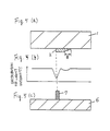
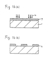
- a light transparent photomask substrate 1 hereinafter referred to merely as “substrate 1" is provided with a phase shifter 2 which is formed by patterning a transparent layer. No light-shielding pattern is formed unlike the conventional photomasks.
- the substrate 1 and the phase shifter 2 in combination are called the “transparent phase-shifter mask”.
- Figure 1 (b) shows the distribution of the intensity of a light passing through the photomask when the latter is irradiated with a light.
- the "transparent phase-shifter mask” is intended to give a phase shift between the light passing through the pattern of the phase shifter 2 and the light passing through the substrate 1.
- the light passing through the phase shifter 2 is shifted in an angular range from 90° to 270°.
- the phase difference can be adjusted by selecting an appropriate thickness of the phase shifter 2.
- the layer is thick enough so as to ensure that the phase difference is 180°M.
- a transparent phase-shifter mask having a phase difference of 180 When a transparent phase-shifter mask having a phase difference of 180 is exposed to light, a light passing through the phase shifter 2 and a light passing through the substrate 1 have a phase difference of 180° to each other, wherein the lights have no substantial phase difference (i.e. coherent lights).
- coherent lights When coherent lights are introduced through different portions, they interact with each other. This interaction affects the light width. If the phase difference is zero, which means that coherent lights passing through the space are mutually in conflict, they strengthen each other. As a result, the sum of the widths of the two lights causes an interference.
- a light passing through the substrate 1 and the phase shifter 2 have a phase difference of 180°. As a result, the two lights cause an interference so as to weaken each other.
- a light passing through both ends of the phase shifter 2 causes an interference with a light passing through an adjacent substrate 1 because of their mutual phase differences being different by 180° so that the mutual light intensities are weakened. In other words, the intensity of light is minimized because of the interference caused by the edges of the phase shifter 2.
- Figure 1 (c) shows an example of forming a positive resist pattern by the use of a photomask according to the present invention.
- a semiconductor substrate 6 is prepared, on which a resist is coated to a thickness of 0.5 microns, and the coat is pre-baked so as to harden the resist.
- the hardened resist is exposed to an irradiation having the intensity shown in Figure 1 (b).
- the exposed portions are removed so as to form a resist pattern 7 with a developer.
- the number of the resist patterns 7 formed on the semiconductor substrate 6 amounts to two times the number of those formed on the substrate 1. It will be understood from this that resolving power is enhanced as compared with the known exposing technique utilizing no phase difference.
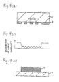
- Figure 2 shows an example of forming a single pattern (hereinafter called "single pattern") as a phase shifter 2.
- Figure 2 (a) is a sectional view showing a transparent phase-shifter mask according to the present invention:
- the single pattern is formed at a sufficient distance from other patterns formed on the substrate 1. Another pattern is also shown which in free from an adverse influence when a resist pattern is formed, even if the light is interfered by a light passing through other patterns on the substrate 1.
- the lights passing through the phase shifter 2 and the substrate 1 have a phase difference.
- Two lights passing through the edges of the phase shifter 2 have a phase difference of 180°, thereby causing an interference which weakens the intensity.
- the distribution of light intensity on a wafer is minimized at the edges of the pattern.
- the resist pattern 7 takes the form shown in Figure 2 (c).
- the area covered with the light-shielding layer remains as a resist pattern.
- the transparent phase-shifter mask has no distinct areas of white (an area through which a light passes) and of black (the area to which a light is shielded).
- the transparent phase-shifter mask allows a light passing through the substrate 1 to pass through, and a light passing through the phase shifter 2 to pass through.
- the present invention requires a light-shielding layer but utilizes the intensity of light varying owing to interference.
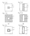
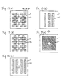
- Figure 3 shows shapes of a phase shifter 2 formed on the substrate 1.
- the resulting positive resist pattern takes the form shown in Figure 3 (c).
- Figure 3 (a) shows a square area given by the phase shifter 2
- Figure 3 (b) shows a larger area given by the phase shifter 2.
- the same resist pattern 7 is formed as shown in Figure 3 (c) by irradiating a laser beam upon the semiconductor substrate 6.
- the transparent phase-shifter mask the resist pattern is formed at an area where the phases of the irradiated light differ by 180°. The intensity of light is reduced at this area, and after development, the resist around this area remains.
- the edge portion of the square phase shifter 2, and other edge portions than the square phase-shifter correspond to the area where the phases are displaced by 180 ⁇ .
- the same shape of resist patterns 7 are formed.
- Figure 3 (d) shows an area formed by a rectangular phase shifter 2 on the substrate 1 and Figure 3 (e) shows an area other than the rectangular portion which is formed by the phase shifter 2.
- the fine pattern shown in Figure 3 (c) is difficult to fabricate by the use of a photomask in common use or a conventional phase shifter mask. That is, if in photomasks made from a conventional light-shielding layer a resist pattern 7 to be formed is rectangular or square, the light-shielding layer must be correspondingly rectangular or square. In this case, electron beams are used to pattern the resist coated on the light-shielding layer.
- a problem arises in that when the rectangular shape to be formed is extremely fine, the area of exposure is likely to expand owing to scattering of electron beams. As a result, the four corners of both rectangles are rounded. When a much finer pattern is to be formed, the square of the resist pattern 7 becomes rounded.
- the desired area is exposed to light by diffraction through the edges of the shielding layer; more specifically, the corners of the square of the resist pattern 7 are rounded or the square remains.
- phase shifter mask Even in the conventional phase-shifter mask the same problem arises because the light-shielding layer is formed and a phase shifter is formed in the edge portion. In contrast, in transparent phase-shifter mask a phase shifter a resist pattern can be formed in a desired shape.
- a resist pattern 7 formed by the use of a transparent phase-shifter mask is formed along the periphery of a pattern of the phase shifter 2. This shapes the phase shifter 2 like an closed ring or alternatively a slightly modified shape. With the use of such shapes of resist patterns 7 alone it is difficult to fabricate intricate patterns such as LSls, and it is required to prepare various shapes other than the closed ring shape.
- phase shifter which diminishes in thickness continuously or step by step.
- this type of phase shifter is called a multi-stage phase shifter, which will be described in detail:
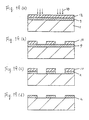
- the phase shifter 2 includes a multi-stage phase shifter 8 which has a left-hand wall constantly upright to the main surface of the substrate 1 and has a right-hand wall gradually changeable in thickness.
- Figure 4 (a) shows the multi-stage phase shifter portion 8 whose one side diminishes toward its end
- Figure 4 (b) shows the phase-shifter whose one side diminishes in thickness step by step; in the illustrated embodiment, the thickness in the step diminishes by 1/2 of the entire thickness
- Figure 4 (c) shows other multi-stage phase shifter 8 whose one side has three steps, diminishing in thickness by 1/4 of the entire thickness.
- the phase of an incident light is 180° at the left end of the phase shifter 2, and makes a phase difference of 180° from the phase of an incident light to an area having no phase shifter.
- the incident light to the right end of the multi-stage phase shifter 8 has a phase difference varying from 180° to 0 (zero) continuously.
- the phase difference of light is 180° in the phase shifter 2, 90° in the multi-stage phase shifter 8, and 0 in the photomask.
- the radiated light has a phase difference of 180° at the left end portion of the phase shifter 2, and its intensity is remarkably reduced.
- the phase difference gradually diminishes, and the reduction of light intensity due to interference is minimized.
- Figure 6 shows the shape of a phase shifter formed on the main surface of the substrate 1, and a resist pattern formed on a semiconductor substrate.
- FIG 6 (a) shows a rectangular phase shifter having a multi-stage phase shifter.
- This type of transparent phase-shifter mask has a phase shifter which gives a phase difference of 180° to the substrate 1.
- the phase shifter 2 has a rectangular shape, and forms a rectangular shape of resist pattern as shown in Figure 3.
- the phase shifter includes a phase shifter 2 and a multi-stage phase shifter 8.
- This multi-stage phase shifter 8 is provided by the edges corresponding to the phase shifter 2 that does not form a desired resist pattern.
- This multi-stage phase shifter 8 is formed along the three edges of the phase shifter 2, and the light intensity in the area enclosed by the multi-stage phase shifters 8 is least reduced, thereby forming no pattern.
- Figure 6 (b) shows a positive resist pattern formed by the use of this type of transparent phase-shifter mask.
- the single resist pattern 7 is formed. If this single resist is to be formed by the use of a conventional photomask, the light will be diffused to area other than a predetermined one under the influence of diffraction. This prevents the resist pattern 7 from being formed in a desired form.
- the conventional phase shifter mask is suitable for fabricating repeated patterns but not suitable for fabricating a single pattern.
- the use of a transparent phase shifter mask enables a single resist pattern to be fabricated easily.
- a multi-stage phase shifter can be used which changes the phase continuously or step by step, thereby allowing the resist patterns to be formed at various places.
- Figures 7 (a) to (d) shows the phase shift pattern of a photomask according to the present invention when it is used to form a resist pattern for a line-and-space.
- FIG 7 (a) shows a phase shifter 2 which gives a phase difference of 180° to the transparent substrate 1.
- the phase shifter 2 is generally rectangular, which forms a rectangular resist pattern as shown in Figure 3.
- the phase shifter includes a phase shifter 2 and a multi-stage phase shifter 8.
- the multi-stage phase shifter 8 is provided at the top portion of the phase shifter 2.
- the widths of a plurality of phase shifters 2 and the widths of a space existing between the phase shifters 2 can be changed.
- FIG 7 (b) shows a phase shifter 2 which gives a phase difference of 180° to a transparent photomask substrate 1.
- This phase shifter 2 is generally rectangular, which forms a rectangular resist pattern as shown in Figure 3.
- the phase shifter includes the phase shifter 2 and a multi-stage shifter 8.
- the multi-stage phase shifter 8 is provided at the top portion of the phase shifter 2.
- the widths of a line and space of a resulting resist pattern In order to change the widths of a line and space of a resulting resist pattern, the widths of a plurality of phase shifters 2 and the width of an area existing between the phase shifters 2.
- Figure 7 (c) shows a reversed structure in which the phase shifter 2 and the photomask substrate 1 shown in Figure 7 (a) are turned upside down as shown in Figure 3. This structure enables the resist pattern to be formed in an identical shape to that of Figure 7 (a).
- Figure 7 (d) shows a reversed structure in which the phase shifter 2 and the photomask substrate 1 shown in Figure 7 (b) are turned upside down as shown in Figure 3.
- This structure enables the resist pattern to be formed in an identical shape to that of Figure 7 (b).
- the resist pattern in a matrix is formed as shown in Figure 8 (b). If the lateral width of the line pattern is to be changed, it is possible to change the lateral width of the plurality of phase shifters 2 and the area existing between the phase shifters 2. If the longitudinal width of the line pattern is to be changed, it is possible to change the vertical thickness of the plurality of multi-stage phase shifters 8.
- the cross-sectional structure is formed as shown in Figure 4 (a) which diminishes in thickness continuously.
- this structure advantageously allows the amount of exposure to be relatively low to such an extent that the thickness of the multi-stage phase shifter 8 be reduced by half when a pattern of the phase shifter 2 is formed by exposure and development.
- the pitch p of a pattern of the phase shifter 2 It depends upon the value of the pitch p of a pattern of the phase shifter 2 whether the resist pattern is formed by the use of a phase shifter 2. More specifically, when the pitch p is sufficiently wide, the light through a transparent phase-shifter mask is least intensified at the edge portion of the pattern of a particular phase shifter 2, and the light intensity is most reduced at an edge portion of the phase shifter 2 at edge portions of a phase shifter adjacent to the first phase shifter 2. If an area between the two phase shifters 2 has a light having an intensity above a particular level, a line and space pattern is formed at the time of development. This particular level means a level at which an optical resolving is possible. In this way the repeated pattern is formed as shown in Figure 1.
- the distribution of light intensity on the substrate 1 lacks contrast, thereby failing to form a resist pattern.
- the lights passing through the pattern of the phase shifter 2 and the substrate 1 interfere with each other thereby weakening each other.
- the distribution of light will be understood from Figure 9 (b) that at the edge portion of the phase shifter 2 having a wide pitch p, the light is least intensified, and the edge portion of the phase shifter 2 adjacent to the first phase shifter 2 is least intensified.
- the light intensity is reduced by the edges of the phase shifter 2. This process is repeated, and the light is intensified at an area where the pitch p becomes wider than the predetermined width.
- the light intensity in a resist pattern for a wider resist pattern is possible.
- the resolution of an optical resist pattern has a limit R, which is represented by the following formula: where k 1 is a constant, X is a wavelength of light, and NA is a numerical aperture of the optical lens.
- k 1 When a conventional photomask is used, k 1 is 0.5. When a conventional shift mask is used, k 1 is 0.35.
- Resolution limits R are compared between when a phase shift is used and when a conventional photomask is used, and it is found that the phase shift mask has a resolution limit R reduced 1.4 times that of a conventional photomask, provided that other conditions than the value k 1 are the same. As a result, the resulting resist pattern has a reduced width.
- resolution limit is under an optical projection system unless specified to the contrary.
- the value of k 1 was about 0.35. This is the same value obtained by the use of the conventional phase shift. This is rational in that the underlying theory of irradiation exposure is the same for forming resist patterns between the use of a conventional phase shift and a transparent phase-shifter mask of the present invention. More specifically, when the phase difference is 180° between a light radiated by the edge of the phase shifter and a light radiated upon a photomask substrate, the light intensity is minimized. When this phenomenon is utilized so as to form a resist pattern, the value of k 1 (resolution limit R) was about 0.35.
- the edge portion of the phase shifter forms a resist pattern.
- a number of resist patterns amounts to twice that of the patterns of the phase shifter.
- the pitch p of the phase shifter patterns calculated from the width of the resist pattern on the semiconductor substrate is Rx4.
- the pitch p is above a resolution limit, the resist pattern will be resolved.
- the pitch of a repeated phase shifter pattern must be not larger than four times the value R.
- the pitch p is preferably in a range of 1.0 to 4.9 am, wherein the pitch of the resist pattern on the semiconductor substrate is in the range of 0.2 to 0.6 am.
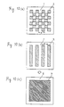
- Figure 11 shows the results of the light-shielding performance of the repeated patterns of the phase shifter.
- the Y-axis indicates a light intensity ratio where I is the light intensity achieved when a light having an intensity of 10 is passed through the transparent phase-shifter mask, and the X-axis indicates the pitch p of the phase shifter pattern.
- White circles indicate the result of the transparent phase-shifter mask when the phase shift pattern are arranged in a line-and-space
- black circles indicate the result of transparent phase-shifter mask when the phase shifter patterns are repeated in a matrix.
- the pitch p is in the range of 1.0 to 3.0 am, the light intensity ratio is within 10%.
- the phase shifter pattern is in a matrix, the light intensity is within 10% if the pitch p is in the range of 1.0 to 4.0 am. In Figure 11, irrespective of increases in the pitch p the light Intensity increases, which indicates that the phase shifter is not shaped as desired.
- the phase shifter having a line-and-space pattern can be used on condition that the pitches p are in the range of 1.0 to 3.0 ⁇ m, and the phase shifter having a matrix pattern can be used on condition that the pitches p are in the range of 1.0 to 4.0 ⁇ m.
- phase shifter patterns having a resolution limit
- various patterns can be formed.
- Figure 12 shows a resist pattern a photomask designed to form a resist pattern in a single form by irradiation exposure and development.
- Figure 12 (a) shows transparent phase-shifter masks disposed in a line-and-space shape at pitches below a resolution limit. A space is provided at an interval I in the phase shifter 2.
- a resist pattern 7 is formed because this area is shielded against an irradiated light, and the resist in the space having the interval I is exposed to an irradiated light passing through the space. In this way the resist pattern 7 has a void portion.
- Figures 13 (a) to (d) show a variety of transparent phase-shifter masks which allow resist patterns to become a hole pattern.
- Figure 13 (a) shows patterns of the phase shifter 2 arranged in a matrix with a pitch p, which is below a resolution limit. One phase shifter 2 in the center is removed, thereby making the entire shape like a cross through which an irradiated light is passed. This cross portion allows an irradiated light to pass through because the pitch is larger than p; more specifically, when an irradiated light passes through the phase shifter 2 and an irradiated light passes through a portion of the photomask substrate 1 which is adjacent to the phase shifter 2, they cancel each other out if their phases are reversed by 180°. If the mutual cancellation occurs, an irradiated light passes through a portion of the phase shifter 2 where the frequency of the light is disturbed, and contributes to exposure, as shown in Figure 13 (a).
- Figure 13 (b) shows patterns of the phase shifter 2 arranged at pitches p on the substrate 1, wherein the pitch p is below a resolution limit.
- the phase shifter 2 takes the form of a cross, which allows an irradiated light to pass through because the pitch is larger than p.
- an irradiated light passes through the phase shifter 2 and an irradiated light passes through a portion of the photomask substrate 1 which is adjacent to the phase shifter 2, they cancel each other out if their phases are reversed by 180°. If the mutual cancellation occurs, an irradiated light passes through a portion of the phase shifter 2 where the frequency of the light is disturbed, and contributes to exposure.
- Figure 13 (c) shows a line-and-space pattern formed on the substrate 1, with a pitch p being below a resolution limit.
- the central portion takes the shape of the letter H, where an irradiated light is passed through because the pitch is larger than p.
- Figure 13 (d) shows a line-and-space pattern formed on the substrate 1, with a pitch p being below a resolution limit.
- the central portion is void.
- the void portion takes the shape of the letter H, where an irradiated light is passed through because the pitch is larger than p.
- Figure 13 (e) shows a resist pattern 7 formed on the semiconductor substrate 6 by radiating a light upon the transparent phase-shifter mask.
- the transparent phase-shifter mask allows part of a light to pass through and makes it contribute to exposure.
- a square resist pattern is formed but in the case of intricate patterns a single resist pattern having a circular void.
- the repetition of intricate phase shifter patterns function as a light-shielding layer such as a chromium layer and molybdic silicide layer.
- the widths of a pattern whose dimension is a degree capable of being resolved by the conventional photomask can be controlled.
- the interval I of the void area of the phase shifter shown in Figure 12 can be changed so as to control the resulting resist pattern.
- this cannot be applied to a case shown in Figure 1 where extremely intricate line-and-space pattern.
- Figure 14 (c) shows a photomask having a first and a second phase shifters 2 crossing each other formed on the substrate 1, wherein the shape of the individual stripes are the same as those shown in shifter are not continuous. More specifically, the stripes of the second phase shifter cross those of the first phase shifter at constant intervals. In other words, each stripe of the first phase shifter 2 has equally spaced projections in opposite directions. These projections act as light-shielders against an irradiated light.
- the resulting patterns have slightly widened stripes as shown in Figure 14 (d), wherein the letters I , m and n indicate the width of each projection, the projecting length, and 1/2 ( t + m), respectively.
- the widths of the resist pattern 7 to be transferred are virtually equal to 2n.
- the area having a width below a resolution limit acts as a light-shielder against an irradiated light. This means that the width of the resulting resist pattern does not depend upon the value of t but on the value of m.
- the light intensity decreases along a sine curve. This is because the resist pattern 7 has a smaller width than the length of the projections.
- Figure 15 (a) shows the sizes of the phase shifter 2, which has a width of 0.8 am. This size is equal to 2n, wherein the n is shown in Figure 14 (c). equal to 2n, wherein the n is shown in Figure 14 (c).
- the width t of the phase shifter 2 shown in Figure 14 (c) is set to 0.2 ⁇ m so that the resulting pattern width may be below a resolution limit.
- the projections have a length of m.
- Figure 15 (b) shows a cross-section of a resist pattern formed by exposure and development by using a transparent phase-shifter mask shown in Figure 15 (a).
- the distance between the resulting resist patterns is equal to 2n.
- the width of the resist pattern means a width w of the bottom of the resist pattern kept in contact with the semiconductor substrate 6 as shown in Figure 15 (b).
- the width w becomes wider in proportion to the length m of the projection.
- the width m of the projections is zero, that is, the case of a stripe-shape phase shifter, the width of the resulting resist pattern becomes about 0.25 am.
- the width of the resulting resist pattern becomes 0.4 ⁇ m.
- the resist pattern becomes narrower in inverse proportion to the length of the projections.
- the width of the resulting resist pattern becomes about 0.48 ⁇ m.
- the width w of the resulting resist pattern becomes 0.4 ⁇ m.
- the width of the resist pattern to be transferred by projection and exposure is virtually equal to 2n.
- the area of a phase shifter having a width below a resolution limit acts as a light-shielding layer against an irradiated light. This indicates that the width of the resulting resist pattern does not depend upon the width t of the phase shifter but upon the length m of the projections.
- the light-shielding area becomes wider in proportion to the length of the projections.
- the width of a resist pattern to be transferred depends upon the length m of the projections.
- Figure 14 (e) shows a phase shifter 2 formed in stripes on the substrate 1 of Figure 14 (a), wherein the phase shifter 2 is provided with a multi-stage phase shifter 8 along the opposite sides thereof.
- m and n indicate the width of the multi-stage phase shifter 8 and 1/2 (the width of the stripe-shape phase shifter 2 + m).
- the value m decides the width of the resist pattern 7 to be projected.
- the width of the resist pattern 7 to be transferred by projection and exposure is virtually equal to 2n.
- the resulting resist pattern 7 becomes thicker in proportion to the value m.
- the width is equal to the sum of the width of the stripe-shaped phase shifter 2 and m. This means that the width of the resist pattern 7 can be controlled by changing the value of m.
- the width of the resist pattern 7 does not exceed the sum of 2m and the width of the stripe-shaped phase shifter 2 is that the light intensity decreases at a sine curve by the edge portions of the projections.
- the resist pattern 7 formed by developing an irradiated area is short of the terminating ends of the projections.
- the light-shielding area becomes wider and results in the pattern shown in Figure 14 (d).
- Figure 14 (f) shows a photomask having a stripe-shaped inner phase shifter 2a on the substrate 1 of Figure 14 (a).
- This inner phase shifter 2a is provided with outer phase shifters 2b along the opposite sides of the inner phase shifter 2a.
- 1, n and m indicate a distance between the centers of the inner phase shifter 2a and the outer phase shifter 2b, the width of the outer phase shifter 2b and an interval between the inner phase shifter 2a and the outer phase shifter 2b, wherein the m and n are below a resolution limit.
- the width of the resist pattern 7 to be transferred by projection and exposure is virtually equal to 2t.
- the width of the resist pattern 7 depends upon the sum of the width n of the outer phase shifter 2b and the interval between the inner and outer phase shifters 2a and 2b.
- the light-shielding area becomes wider in proportion to the width n of the outer phase shifter 2b and/or the interval between the inner and outer phase shifters 2a and 2b, provided that both values of m and n are below a resolution limit. If the sum of m and n are set to an excessively large value, either of them will come to exceed the resolution limit. In such cases, it is preferable that the pattern consisting of the inner and outer phase shifters 2a and 2b with intervals therebetween should be repeated.
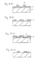
- a process of fabricating the transparent phase-shifter mask will be described by way of examples: A first example will be described by reference to Figure 16 (a).
- a quartz substrate 1 is prepared, and a transparent electroconductive layer such as indium tin oxide (hereinafter called ITO layer) is deposited to a thickness of 0.1 ⁇ m on the substrate 1.
- ITO layer indium tin oxide
- a transparent layer 9 is spin-coated on the substrate 1 as a phase shifter 2.
- PMMA layer polymethyl methacrylate
- an exposing radiation is applied through electron beams 10 at an accelerating voltage 25 KV by the amount of exposure of about 130 u.C/cm 2.
- the radiated surface is sprayed with a mixture methylisobutyl ketone (hereinafter called MIBX) and isopropyl alcohol (hereinafter called IPA) at a ratio of 1:2 for three minutes so as to effect development.
- MIBX mixture methylisobutyl ketone
- IPA isopropyl alcohol
- the development dissolves the exposed part to form a desired pattern.
- the substrate 1 is rinsed with IPA, and spin-dried. In this way the transparent phase-shifter mask of Figure 16 (b) is formed.
- the substrate 1 is covered with an ITO layer to form a desired pattern of PMMA.
- This ITO layer of electroconductivity is effective to prevent electrons from accumulating in the substrate 1 which is inherently an insulator allowing the accumulation of electrons in the substrate 1. The accumulated electrons are likely to disturb the electron beams 10, thereby distorting a resulting pattern.
- the ITO layer can be only thick so as not to affect the exposure of the substrate 1 unfavorably.
- the PMMA layer is sufficiently thick so as to inverse the phase of an irradiated light by 180 ⁇ .
- a second example will be described by reference to Figure 17, which is different from the first example in that multi-stage phase shifter 8 is used.
- a substrate 1 of quartz is prepared, and a transparent layer 9 is deposited on the substrate 1.
- a PMMA layer is spin-coated to a thickness of 0.372 ⁇ m.
- an exposing radiation is applied through electron beams 10 at an accelerating voltage 25 KV by the amount of exposure of about 130 ⁇ C/cm 2 .
- the amount of exposure applied thereto is adjusted to 50 ⁇ c/cm 2 .
- the amounts of exposure are set to 45 and 60 ⁇ C/cm 2 .
- PMMA is used for the phase shifter 2 which is an organic layer but PMMA may involve a problem of durability; more specifically, when in using a transparent phase-shifter mask to effect a radiating exposure, KrF excimer laser or any other far ultra-violet ray (having a wavelength of 200 nm to 300 nm) is used as a source of light, the problem is often caused because the far ultra-violet ray generates high energy owing to its relatively short wavelength and causes the ablation of the PMMA layer.
- an effective chemical formula is shown in Figure 18.
- Figure 18 (a) shows the chemical formula of salt-onium that can be used as a photosensitive agent.
- Figure 18 (b) shows polysiloxane having a ladder structure used as a base resin.
- the resist used in the example contains a mixture of polysiloxane of Figure 18 (b) as a base resin and a salt- omiun of Figure 18 (a) by 0 to 10 part by weight.
- This resist has a high sensitivity of 0.2 ⁇ C/cm 2 to the electron beams, and therefore it is possible to use this resist for the phase shifter instead of the PMMA.
- a stable phase shifter can be produced by a simple process.
- any other substance can be used if it consists mainly of polysiloxane having a silicon-base chain structure.
- Any other agent having such a base resin and having a sensitivity to electron beams can be used as a resist and a phase shifter.
- chloromethylated polysiloxane and clear polymers such as silicon resins containing highly reactive end groups can be used.
- a silicon nitride layer 9 is formed on the substrate 1 to a thickness of about 0.18 ⁇ m by sputtering, followed by the spin-coating of a CMS layer 12 to a thickness of about 0.5 ⁇ m. Then, the CMS layer 12 is heated at 120° C for 30 minutes and hardened.
- the next step is to expose the desired pattern by using electron beams 10 by an amount of exposure of 6 ⁇ 2 . Then a mixture of isopentyle acetate and ethylene glycol monoethyl ether is sprayed for a minute so as to effect development. In this way the resist pattern 13 is formed as shown in Figure 19 (b).
- the silicon nitride layer 9 is dry etched by using a mixture of CF 4 and 0 2 whereby the silicon nitride layer 9 is removed, and the substrate 1 is exposed. The process so far is shown in Figure 19 (c).
- the final step is to remove the resist pattern 13 with an oxygen plasma, so as to form the phase shifter 2 of the silicon nitride layer 9.
- the transparent phase-shifter mask is formed as shown in Figure 19 (d).
- the next step is to deposit a transparent layer 9 such as a silicon oxide layer to a thickness of 0.47 ⁇ m by vacuum vapor deposition using electron beams, thereby forming a phase shifter 2.
- a transparent layer 9 such as a silicon oxide layer to a thickness of 0.47 ⁇ m by vacuum vapor deposition using electron beams, thereby forming a phase shifter 2.
- the resist pattern 13 is removed by submerging the substrate 1 in aceton, and at the same time the silicon oxide layer on the resist pattern is also removed. However, the silicon oxide layer deposited directly on the substrate 1 remains on the substrate 1. In this way a transparent phase-shifter mask having the phase shifter 2 of silicon oxide layer is formed.
- Figure 21 (a) shows the transparent phase-shifter mask used in the above-mentioned process, indicating the pattern of the phase shifter 2.
- Figure 21 (b) shows the resist pattern 7 formed on the semiconductor substrate 6 in the above-mentioned manner.
- the phase shifter 2 has stripes, hereinafter called “stripe-shaped phase shifter”.
- the resist pattern 7 has two times as many stripes as those of the phase shifter 2.
- the process using a transparent phase-shifter mask according to the present invention is more advantageous than a process without using any phase shifter, in that the former can achieve a line-and-space pattern with 0.3 ⁇ m in intervals whereas the latter produces it only with 0.45 ⁇ m in intervals. Furthermore, the latter process cannot constantly form single patterns with fineness of below 0.5 /1.m. According to the former process, it is possible to produce single patterns with fineness of 0.3 ⁇ m constantly.
- a light passing through edge portions of the phase shifters 2 effects exposure.
- Lights passing through the rectangular phase shifters 2 and through the rectangular substrate portions adjacent thereto have phases in reverse to each other, thereby reducing the light intensity.
- the rectangular phase shifter 2 and the rectangular substrate portions provide a light-shielding area in combination against the irradiated light.
- phase shifter 2 Without using the phase shifter 2 the resulting contact hole is only 0.55 ⁇ m, whereas the transparent phase-shifter mask enables the formation of contact hole of 0.4 /1 .m.
- Figure 21 (e) shows a transparent phase-shifter mask used for forming a pattern which becomes a capacitor in which rectangular phase shifters 2 and rectangular substrate portions are formed in repeated patterns.
- Figure 12 (f) shows the resist pattern formed by using the photomask of
- a negative resist is used. Reversely to the examples described above, the exposed area remains as a resist pattern 7 on the semiconductor substrate 6. That is, an area where the light intensity is reduced is developed.
- Figure 21 (g) shows a transparent phase-shifter mask used for forming a pattern allowing the formation of an element separating areas.
- This pattern includes a step-shaped area and a void-present area which includes a space at the center.
- the substrate 1 includes a stepped area in the substrate, and a stepped area in the pattern.
- the phase shifter portion adjacent to the space, and the substrate portion adjacent to the phase shifter have narrow widths. It is necessary to reduce the size of these narrow areas so as to be below a resolution limit.
- resist patterns 7 to be transferred to the negative resist are shown in Figure 21 (h) where the pattern is formed by the removal of the resist in the non-exposed area.
- the patterns shown in Figures 21 (g), 21 (i), and 21 (j) can be selected in accordance with a desired shape of the light-shielding areas where the pattern is formed below a resolution limit.
- an area is provided where the phase shifter 2 is formed in the substrate 1 and an area where a void is formed in the phase shifter 2, thereby forming a pattern incapable of resolution.
- an area is provided where a phase shifter portion is formed in the area of the substrate 1 in which the phase shifter 2 is formed in the substrate 1 and where the substrate portion is formed in the phase shifter 2, thereby forming a pattern incapable of resolution.
- the phase shifter 2 includes areas having two side lines. Each side line of each area is parallel to an adjacent side line of an adjacent area. If the interval between one side line and an adjacent side line is below a resolution limit, this area acts as a light-shielder against an irradiated light. Likewise, if the intervals between the phase shifter 2 and the substrate portion is below a resolution limit, this area acts as a light shielder against an irradiated light.
- the area 17 is formed by a repetition of phase shifter portions incapable of resolution. When a light is radiated, the light intensity in the area 16 is reduced by each side of the rectangular shape. When a negative resist is used, the resist along the edges of the area 16 is reduced. The other area 17 acts as a light-shielder against an irradiated light, thereby making a portion devoid of a resist.
- Figure 23 (b) shows a state where the a pattern described above is transferred onto a negative resist by the use of a transparent phase-shifter mask.
- the area 16 forms a photoelectric converter for a CCD solid image pickup device
- the area 17 forms a vertical transfer channel for reading out an electric charge stored by the photoelectric converter.
- Intricate fine lines are formed in the vertical transfer channel by the edge portions of the area 16 but such fine lines do not unfavorably affect the characteristics of the vertical transfer channel. If there is a worry about any unfavorable influence, the provision of the multi-stage phase shifter along the longer sides of the rectangular area 16 will eliminated the possibility of forming fine lines in the transfer channel.
- the intervals between the resist patterns are about 0.2 /1 .m at minimum, and in areas where the intervals are wider, the repetition of patterns having a width below a resolution limit is used so as simplify the step for fabricating gates.
- An area 18 is where a take-out electrode 19 is where a gate is formed.
- the area 18 is constituted by intricate phase shifter portions 2a, and rectangular phase shifter portions 2b have widths below the resolution limit, thereby becoming a light-shielder against an irradiated light.
- the rectangular phase shifter portions 2b the light intensity is reduced on the edge portions, thereby enabling a straight gate to be formed along the edges of the phase shifter portions 2b.
- a resist pattern should not be formed along the three sides other than the side along which the gate is formed.
- multi-stage phase shifters 8 are preferably formed along them.
- phase-shifter mask By using this transparent phase-shifter mask a resist pattern is formed by exposure on the semiconductor substrate 6.
- a negative resist is used so that the area 18 and the rectangular phase shifter potions 2b forming the gate include a light-shielder against an irradiated light. The light-shielding portions get rid of the resist after exposure and development.
- Redundant patterns formed along the phase shifter 2 are negated by using multi-stage phase shifter 8.
- a large-size electrode to the gate is formed by using the pattern of the phase shifter 2 below a resolution limit.
- This type of transparent phase-shifter mask enables the fabrication of a semiconductor device of GaAs having a gate width of 0.15 /1.m. Under the conventional method an electron beam drawing process was used to form intricate fine patterns, but because of the necessity of using vacuum, the process was not suitable for the mass-production.
- PMMA, siloxane- polymer base resists, silicon nitride layers and silicon oxide layers are used but magnesium fluoride, titanium dioxide, titanium nitride or any other transparent polymers can be used.
- phase shifter used in an exposing device having a wavelength for exposure of 365 nm but any other exposing device can be used if the following equation is satisfied: where t is the thickness of the phase shifter, and n is a diffraction index of the phase shifter.
- phase shifter mask consists of patterns formed a transparent photomask substrate for a transparent phase shifter.
- Figure 25 shows a photomask having a light-shielding area using a phase shifter and a light-shielding layer such as a chromium layer in combination.
- the resulting light-shielding pattern will be described by referring to Figure 25:
- a rectangular phase shifter 2 has an edge where the light intensity is reduced, thereby for ming a straight gate along the edge. No resist pattern should be formed along the three sides other than the side along which the gate is formed. In order to achieve it, multi-stage phase shifters 8 are formed along them.
- a resist pattern is formed by exposure on the semiconductor substrate 6.
- a negative resist is used so that the area 28 and the rectangular phase shifter 2 forming the gate include a light-shielder against an irradiated light. The light-shielding portions get rid of the resist after exposure and development.
- Redundant patterns formed along the phase shifter 2 are negated by using multi-stage phase shifter 8.
- a large-size electrode to the gate is formed by using the pattern of the phase shifter 2 below a resolution limit.
- This type of transparent phase-shifter mask enables the fabrication of a semiconductor device of GaAs having a gate width of 0.15 /1.m. Under the conventional method an electron beam drawing process was used to form intricate fine patterns, but because of the necessity of using a vacuum, the process was not suitable for mass-production.
- phase shifter instead of using a transparent phase-shifter mask for a phase shift mask, it is possible to use a phase shifter and a light-shielding layer such as a chromium layer in combination.
Landscapes
- Physics & Mathematics (AREA)
- General Physics & Mathematics (AREA)
- Health & Medical Sciences (AREA)
- Engineering & Computer Science (AREA)
- Environmental & Geological Engineering (AREA)
- Epidemiology (AREA)
- Public Health (AREA)
- Preparing Plates And Mask In Photomechanical Process (AREA)
- Exposure And Positioning Against Photoresist Photosensitive Materials (AREA)
Applications Claiming Priority (3)
| Application Number | Priority Date | Filing Date | Title |
|---|---|---|---|
| JP16334390 | 1990-06-21 | ||
| JP16334390 | 1990-06-21 | ||
| JP163343/90 | 1990-06-21 |
Publications (2)
| Publication Number | Publication Date |
|---|---|
| EP0464492A1 true EP0464492A1 (de) | 1992-01-08 |
| EP0464492B1 EP0464492B1 (de) | 1999-08-04 |
Family
ID=15772074
Family Applications (1)
| Application Number | Title | Priority Date | Filing Date |
|---|---|---|---|
| EP91110167A Expired - Lifetime EP0464492B1 (de) | 1990-06-21 | 1991-06-20 | Photomaske, die in der Photolithographie benutzt wird und ein Herstellungsverfahren derselben |
Country Status (5)
| Country | Link |
|---|---|
| US (2) | US5605775A (de) |
| EP (1) | EP0464492B1 (de) |
| KR (1) | KR950002871B1 (de) |
| DE (1) | DE69131497T2 (de) |
| TW (1) | TW198129B (de) |
Cited By (37)
| Publication number | Priority date | Publication date | Assignee | Title |
|---|---|---|---|---|
| EP0477035A2 (de) * | 1990-09-21 | 1992-03-25 | Dai Nippon Printing Co., Ltd. | Phasenverschiebungs-Photomaske, Herstellung und Korrektur |
| EP0532040A1 (de) * | 1991-09-12 | 1993-03-17 | Etec Systems, Inc. | Herstellung einer Phasenverschiebungsphotomaske mit unterbrochenen Bereichen |
| EP0534463A2 (de) * | 1991-09-27 | 1993-03-31 | Fujitsu Limited | Belichtungsverfahren mit Phasenverschiebung und Photomaske dazu |
| EP0553543A1 (de) * | 1992-01-31 | 1993-08-04 | Mitsubishi Denki Kabushiki Kaisha | Verfahren zur Erzeugung eines Fotolackmusters |
| EP0620498A1 (de) * | 1993-04-02 | 1994-10-19 | International Business Machines Corporation | Durchsichtige, lithographische Phasenverschiebungsmaske um angrenzenden Strukturen, aus nicht angrenzenden Maskenzonen, zu schreiben |
| EP0980542A1 (de) * | 1998-03-17 | 2000-02-23 | ASML Masktools Netherlands B.V. | Verfahren zur erzeugung von sub-0,25 lambda linien mittels einer gedämpften phasenschiebermaske mit hoher transmission |
| EP1035434A2 (de) * | 1999-03-11 | 2000-09-13 | Infineon Technologies North America Corp. | Photomaske mit nicht aufgelösten Hilfsmustern |
| WO2001022164A1 (de) * | 1999-09-17 | 2001-03-29 | Infineon Technologies Ag | Kontaktlochherstellung mit hilfe sich kreuzender phasensprungkanten einer einzigen phasenmaske |
| WO2001063864A2 (en) * | 2000-02-22 | 2001-08-30 | Micron Technology, Inc. | Chromeless alternating phase-shift reticle for producing semiconductor device features |
| EP1150171A2 (de) * | 2000-04-28 | 2001-10-31 | Infineon Technologies North America Corp. | Gruppierung von Unterstrukturen eines Maskenmusters zur Reduzierung der Linienschrumpfung und zur Verbesserung der Mustergenauigkeit |
| WO2002003140A1 (en) * | 2000-07-05 | 2002-01-10 | Numerical Technologies, Inc. | Phase shift masking for complex patterns |
| US6436590B2 (en) | 1996-09-18 | 2002-08-20 | Numerical Technologies, Inc. | Phase shifting circuit manufacture method and apparatus |
| WO2002075454A2 (en) * | 2001-03-16 | 2002-09-26 | Numerical Technologies, Inc. | Self-aligned fabrication technique for tri-tone attenuated phase-shifting masks |
| WO2002088843A2 (en) * | 2001-04-24 | 2002-11-07 | Canon Kabushiki Kaisha | Exposure method and apparatus |
| US6523165B2 (en) | 2001-07-13 | 2003-02-18 | Numerical Technologies, Inc. | Alternating phase shift mask design conflict resolution |
| US6524752B1 (en) | 2000-07-05 | 2003-02-25 | Numerical Technologies, Inc. | Phase shift masking for intersecting lines |
| US6539521B1 (en) | 2000-09-29 | 2003-03-25 | Numerical Technologies, Inc. | Dissection of corners in a fabrication layout for correcting proximity effects |
| US6541165B1 (en) | 2000-07-05 | 2003-04-01 | Numerical Technologies, Inc. | Phase shift mask sub-resolution assist features |
| US6566019B2 (en) | 2001-04-03 | 2003-05-20 | Numerical Technologies, Inc. | Using double exposure effects during phase shifting to control line end shortening |
| US6569583B2 (en) | 2001-05-04 | 2003-05-27 | Numerical Technologies, Inc. | Method and apparatus for using phase shifter cutbacks to resolve phase shifter conflicts |
| US6573010B2 (en) | 2001-04-03 | 2003-06-03 | Numerical Technologies, Inc. | Method and apparatus for reducing incidental exposure by using a phase shifter with a variable regulator |
| US6584610B1 (en) | 2000-10-25 | 2003-06-24 | Numerical Technologies, Inc. | Incrementally resolved phase-shift conflicts in layouts for phase-shifted features |
| US6593038B2 (en) | 2001-05-04 | 2003-07-15 | Numerical Technologies, Inc. | Method and apparatus for reducing color conflicts during trim generation for phase shifters |
| US6622288B1 (en) | 2000-10-25 | 2003-09-16 | Numerical Technologies, Inc. | Conflict sensitive compaction for resolving phase-shift conflicts in layouts for phase-shifted features |
| DE19545163C2 (de) * | 1994-12-02 | 2003-10-02 | Hyundai Electronics Ind | Phasenschiebermaske zur Bildung von Kontaktlöchern mit Mikroabmessung |
| US6635393B2 (en) | 2001-03-23 | 2003-10-21 | Numerical Technologies, Inc. | Blank for alternating PSM photomask with charge dissipation layer |
| US6653026B2 (en) | 2000-12-20 | 2003-11-25 | Numerical Technologies, Inc. | Structure and method of correcting proximity effects in a tri-tone attenuated phase-shifting mask |
| US6664009B2 (en) | 2001-07-27 | 2003-12-16 | Numerical Technologies, Inc. | Method and apparatus for allowing phase conflicts in phase shifting mask and chromeless phase edges |
| US6681379B2 (en) | 2000-07-05 | 2004-01-20 | Numerical Technologies, Inc. | Phase shifting design and layout for static random access memory |
| US6698007B2 (en) | 2001-10-09 | 2004-02-24 | Numerical Technologies, Inc. | Method and apparatus for resolving coloring conflicts between phase shifters |
| US6735752B2 (en) | 2001-09-10 | 2004-05-11 | Numerical Technologies, Inc. | Modifying a hierarchical representation of a circuit to process features created by interactions between cells |
| US6738958B2 (en) | 2001-09-10 | 2004-05-18 | Numerical Technologies, Inc. | Modifying a hierarchical representation of a circuit to process composite gates |
| US6777141B2 (en) | 2000-07-05 | 2004-08-17 | Numerical Technologies, Inc. | Phase shift mask including sub-resolution assist features for isolated spaces |
| US6852471B2 (en) | 2001-06-08 | 2005-02-08 | Numerical Technologies, Inc. | Exposure control for phase shifting photolithographic masks |
| US7083879B2 (en) | 2001-06-08 | 2006-08-01 | Synopsys, Inc. | Phase conflict resolution for photolithographic masks |
| US7348108B2 (en) | 2000-07-05 | 2008-03-25 | Synopsys, Inc. | Design and layout of phase shifting photolithographic masks |
| CN102759851A (zh) * | 2011-04-25 | 2012-10-31 | 超科技公司 | 有辅助相位区的相移掩模 |
Families Citing this family (22)
| Publication number | Priority date | Publication date | Assignee | Title |
|---|---|---|---|---|
| KR0160924B1 (ko) * | 1995-06-30 | 1998-12-15 | 김주용 | 노광 마스크 |
| JP3053072B2 (ja) * | 1996-09-10 | 2000-06-19 | 東京応化工業株式会社 | レジスト積層体及びそれを用いたパターン形成方法 |
| JPH1092714A (ja) * | 1996-09-11 | 1998-04-10 | Mitsubishi Electric Corp | 半導体装置およびその製造方法 |
| JP4294745B2 (ja) | 1997-09-26 | 2009-07-15 | 株式会社半導体エネルギー研究所 | 光電変換装置の作製方法 |
| US6114071A (en) * | 1997-11-24 | 2000-09-05 | Asml Masktools Netherlands B.V. | Method of fine feature edge tuning with optically-halftoned mask |
| US6121626A (en) * | 1998-09-17 | 2000-09-19 | Vanguard International Semiconductor Corporation | Method and system of exposure with a universal dynamic mask and charge coupled device image feedback control |
| TW497165B (en) | 1999-06-30 | 2002-08-01 | Hitachi Ltd | Method for manufacturing semiconductor integrated circuit device, optical mask used therefor, method for manufacturing the same, and mask blanks used therefor |
| JP3507374B2 (ja) * | 1999-09-03 | 2004-03-15 | キヤノン株式会社 | 二次元位相素子の作製方法 |
| TW512424B (en) | 2000-05-01 | 2002-12-01 | Asml Masktools Bv | Hybrid phase-shift mask |
| US6866971B2 (en) * | 2000-09-26 | 2005-03-15 | Synopsys, Inc. | Full phase shifting mask in damascene process |
| JP2002131884A (ja) * | 2000-10-30 | 2002-05-09 | Hitachi Ltd | フォトマスクの製造方法、フォトマスクおよび半導体集積回路装置の製造方法 |
| EP1288716A1 (de) * | 2001-08-28 | 2003-03-05 | Infineon Technologies AG | Phasenschiebermaske |
| US6684382B2 (en) | 2001-08-31 | 2004-01-27 | Numerical Technologies, Inc. | Microloading effect correction |
| US6548417B2 (en) * | 2001-09-19 | 2003-04-15 | Intel Corporation | In-situ balancing for phase-shifting mask |
| US6841310B2 (en) * | 2002-02-05 | 2005-01-11 | Micron Technology, Inc. | Radiation patterning tools, and methods of forming radiation patterning tools |
| TWI292857B (en) * | 2002-03-25 | 2008-01-21 | Asml Masktools Bv | A method and apparatus for defining mask patterns utilizing a spatial frequency doubling technique |
| TW548718B (en) * | 2002-07-18 | 2003-08-21 | Macronix Int Co Ltd | Hole forming by cross-shape image exposure |
| ATE328303T1 (de) * | 2002-07-26 | 2006-06-15 | Asml Masktools Bv | Richtungsabhängige abschirmung zur benutzung mit dipolbelichtung |
| US7172838B2 (en) * | 2002-09-27 | 2007-02-06 | Wilhelm Maurer | Chromeless phase mask layout generation |
| US20100182580A1 (en) * | 2009-01-16 | 2010-07-22 | Micron Technology, Inc. | Photolithography systems with local exposure correction and associated methods |
| KR20100131117A (ko) * | 2009-06-05 | 2010-12-15 | 삼성모바일디스플레이주식회사 | 유기전계 발광 표시장치용 포토마스크 제조방법 |
| CN113296352B (zh) * | 2020-02-22 | 2023-01-24 | 长鑫存储技术有限公司 | 应用于半导体光刻工艺中的掩膜图形及光刻工艺方法 |
Citations (5)
| Publication number | Priority date | Publication date | Assignee | Title |
|---|---|---|---|---|
| DE2260229B2 (de) * | 1971-12-08 | 1979-07-12 | Nippon Kogaku K.K., Tokio | |
| FR2590376A1 (fr) * | 1985-11-21 | 1987-05-22 | Dumant Jean Marc | Procede de masquage et masque utilise |
| EP0383534A2 (de) * | 1989-02-13 | 1990-08-22 | Kabushiki Kaisha Toshiba | Belichtungsmaske, Herstellungsverfahren und Belichtungsverfahren damit |
| EP0395425A2 (de) * | 1989-04-28 | 1990-10-31 | Fujitsu Limited | Maske, Herstellungsverfahren und Musterherstellung mit einer solchen Maske |
| EP0401795A2 (de) * | 1989-06-08 | 1990-12-12 | Oki Electric Industry Company, Limited | Phasenverschiebungs-Photomaske für negative Lacke und Verfahren zur Herstellung von isolierten negativen Resistbildern mit dieser Phasenverschiebungsmaske |
Family Cites Families (12)
| Publication number | Priority date | Publication date | Assignee | Title |
|---|---|---|---|---|
| AT382040B (de) * | 1983-03-01 | 1986-12-29 | Guenther Stangl | Verfahren zur herstellung von optisch strukturierten filtern fuer elektromagnetische strahlung und optisch strukturierter filter |
| US4759616A (en) * | 1985-08-26 | 1988-07-26 | Eastman Kodak Company | Method and apparatus for anamorphically shaping and deflecting electromagnetic beams |
| JPS6259296A (ja) * | 1985-09-10 | 1987-03-14 | Green Cross Corp:The | ペプタイド誘導体 |
| JPH0738372B2 (ja) * | 1985-10-18 | 1995-04-26 | 工業技術院長 | パタンの形成方法 |
| JPH0690507B2 (ja) * | 1986-02-17 | 1994-11-14 | 株式会社日立製作所 | ホトマスク,及びそれを用いた投影露光方法、並びにホトマスクの製造方法 |
| JPS62259296A (ja) * | 1986-05-06 | 1987-11-11 | Matsushita Electric Ind Co Ltd | 光読出しメモリ |
| JPS6370203A (ja) * | 1986-09-11 | 1988-03-30 | Brother Ind Ltd | 屈折率分布型光導波路レンズの製造方法 |
| JP2710967B2 (ja) * | 1988-11-22 | 1998-02-10 | 株式会社日立製作所 | 集積回路装置の製造方法 |
| JP2864570B2 (ja) * | 1989-10-27 | 1999-03-03 | ソニー株式会社 | 露光マスク及び露光方法 |
| KR950000091B1 (ko) * | 1990-06-20 | 1995-01-09 | 후지쓰 가부시끼가이샤 | 위상 천이기가 있는 레티클과 그 제조방법 및 수정방법 |
| US5100503A (en) * | 1990-09-14 | 1992-03-31 | Ncr Corporation | Silica-based anti-reflective planarizing layer |
| JP2851216B2 (ja) * | 1992-10-16 | 1999-01-27 | キヤノン株式会社 | 画像形成装置 |
-
1991
- 1991-06-20 EP EP91110167A patent/EP0464492B1/de not_active Expired - Lifetime
- 1991-06-20 DE DE69131497T patent/DE69131497T2/de not_active Expired - Fee Related
- 1991-06-20 TW TW080104793A patent/TW198129B/zh active
- 1991-06-21 KR KR1019910010319A patent/KR950002871B1/ko not_active IP Right Cessation
-
1993
- 1993-06-24 US US08/081,835 patent/US5605775A/en not_active Expired - Lifetime
-
1995
- 1995-05-23 US US08/447,781 patent/US5629113A/en not_active Expired - Fee Related
Patent Citations (5)
| Publication number | Priority date | Publication date | Assignee | Title |
|---|---|---|---|---|
| DE2260229B2 (de) * | 1971-12-08 | 1979-07-12 | Nippon Kogaku K.K., Tokio | |
| FR2590376A1 (fr) * | 1985-11-21 | 1987-05-22 | Dumant Jean Marc | Procede de masquage et masque utilise |
| EP0383534A2 (de) * | 1989-02-13 | 1990-08-22 | Kabushiki Kaisha Toshiba | Belichtungsmaske, Herstellungsverfahren und Belichtungsverfahren damit |
| EP0395425A2 (de) * | 1989-04-28 | 1990-10-31 | Fujitsu Limited | Maske, Herstellungsverfahren und Musterherstellung mit einer solchen Maske |
| EP0401795A2 (de) * | 1989-06-08 | 1990-12-12 | Oki Electric Industry Company, Limited | Phasenverschiebungs-Photomaske für negative Lacke und Verfahren zur Herstellung von isolierten negativen Resistbildern mit dieser Phasenverschiebungsmaske |
Cited By (62)
| Publication number | Priority date | Publication date | Assignee | Title |
|---|---|---|---|---|
| EP0477035A3 (en) * | 1990-09-21 | 1992-10-21 | Dai Nippon Printing Co., Ltd. | Phase shift layer-containing photomask, and its production and correction |
| EP0477035A2 (de) * | 1990-09-21 | 1992-03-25 | Dai Nippon Printing Co., Ltd. | Phasenverschiebungs-Photomaske, Herstellung und Korrektur |
| EP0532040A1 (de) * | 1991-09-12 | 1993-03-17 | Etec Systems, Inc. | Herstellung einer Phasenverschiebungsphotomaske mit unterbrochenen Bereichen |
| US5246800A (en) * | 1991-09-12 | 1993-09-21 | Etec Systems, Inc. | Discrete phase shift mask writing |
| US5364716A (en) * | 1991-09-27 | 1994-11-15 | Fujitsu Limited | Pattern exposing method using phase shift and mask used therefor |
| EP0534463A2 (de) * | 1991-09-27 | 1993-03-31 | Fujitsu Limited | Belichtungsverfahren mit Phasenverschiebung und Photomaske dazu |
| EP0534463A3 (de) * | 1991-09-27 | 1994-03-02 | Fujitsu Ltd | |
| US5472813A (en) * | 1991-09-27 | 1995-12-05 | Fujitsu Limited | Pattern exposing method using phase shift and mask used therefor |
| EP0553543A1 (de) * | 1992-01-31 | 1993-08-04 | Mitsubishi Denki Kabushiki Kaisha | Verfahren zur Erzeugung eines Fotolackmusters |
| EP0620498A1 (de) * | 1993-04-02 | 1994-10-19 | International Business Machines Corporation | Durchsichtige, lithographische Phasenverschiebungsmaske um angrenzenden Strukturen, aus nicht angrenzenden Maskenzonen, zu schreiben |
| DE19545163C2 (de) * | 1994-12-02 | 2003-10-02 | Hyundai Electronics Ind | Phasenschiebermaske zur Bildung von Kontaktlöchern mit Mikroabmessung |
| US6566023B2 (en) | 1996-09-18 | 2003-05-20 | Numerical Technology, Inc. | Phase shifting circuit manufacture method and apparatus |
| US6436590B2 (en) | 1996-09-18 | 2002-08-20 | Numerical Technologies, Inc. | Phase shifting circuit manufacture method and apparatus |
| US6818385B2 (en) | 1996-09-18 | 2004-11-16 | Numerical Technologies, Inc. | Phase shifting circuit manufacture method and apparatus |
| EP0980542A1 (de) * | 1998-03-17 | 2000-02-23 | ASML Masktools Netherlands B.V. | Verfahren zur erzeugung von sub-0,25 lambda linien mittels einer gedämpften phasenschiebermaske mit hoher transmission |
| EP0980542A4 (de) * | 1998-03-17 | 2006-03-01 | Asml Masktools Bv | Verfahren zur erzeugung von sub-0,25 lambda linien mittels einer gedämpften phasenschiebermaske mit hoher transmission |
| EP1035434A2 (de) * | 1999-03-11 | 2000-09-13 | Infineon Technologies North America Corp. | Photomaske mit nicht aufgelösten Hilfsmustern |
| EP1035434A3 (de) * | 1999-03-11 | 2001-04-18 | Infineon Technologies North America Corp. | Photomaske mit nicht aufgelösten Hilfsmustern |
| WO2001022164A1 (de) * | 1999-09-17 | 2001-03-29 | Infineon Technologies Ag | Kontaktlochherstellung mit hilfe sich kreuzender phasensprungkanten einer einzigen phasenmaske |
| US6376130B1 (en) | 2000-02-22 | 2002-04-23 | Micron Technology, Inc. | Chromeless alternating reticle for producing semiconductor device features |
| WO2001063864A3 (en) * | 2000-02-22 | 2002-03-21 | Micron Technology Inc | Chromeless alternating phase-shift reticle for producing semiconductor device features |
| WO2001063864A2 (en) * | 2000-02-22 | 2001-08-30 | Micron Technology, Inc. | Chromeless alternating phase-shift reticle for producing semiconductor device features |
| EP1150171A3 (de) * | 2000-04-28 | 2003-08-27 | Infineon Technologies North America Corp. | Gruppierung von Unterstrukturen eines Maskenmusters zur Reduzierung der Linienschrumpfung und zur Verbesserung der Mustergenauigkeit |
| EP1150171A2 (de) * | 2000-04-28 | 2001-10-31 | Infineon Technologies North America Corp. | Gruppierung von Unterstrukturen eines Maskenmusters zur Reduzierung der Linienschrumpfung und zur Verbesserung der Mustergenauigkeit |
| US6503666B1 (en) | 2000-07-05 | 2003-01-07 | Numerical Technologies, Inc. | Phase shift masking for complex patterns |
| US6610449B2 (en) | 2000-07-05 | 2003-08-26 | Numerical Technologies, Inc. | Phase shift masking for “double-T” intersecting lines |
| US6541165B1 (en) | 2000-07-05 | 2003-04-01 | Numerical Technologies, Inc. | Phase shift mask sub-resolution assist features |
| US6681379B2 (en) | 2000-07-05 | 2004-01-20 | Numerical Technologies, Inc. | Phase shifting design and layout for static random access memory |
| US6524752B1 (en) | 2000-07-05 | 2003-02-25 | Numerical Technologies, Inc. | Phase shift masking for intersecting lines |
| US7435513B2 (en) | 2000-07-05 | 2008-10-14 | Synopsys, Inc. | Design and layout of phase shifting photolithographic masks |
| US7348108B2 (en) | 2000-07-05 | 2008-03-25 | Synopsys, Inc. | Design and layout of phase shifting photolithographic masks |
| US7585595B2 (en) | 2000-07-05 | 2009-09-08 | Synopsys, Inc. | Phase shift mask including sub-resolution assist features for isolated spaces |
| WO2002003140A1 (en) * | 2000-07-05 | 2002-01-10 | Numerical Technologies, Inc. | Phase shift masking for complex patterns |
| US6777141B2 (en) | 2000-07-05 | 2004-08-17 | Numerical Technologies, Inc. | Phase shift mask including sub-resolution assist features for isolated spaces |
| US6539521B1 (en) | 2000-09-29 | 2003-03-25 | Numerical Technologies, Inc. | Dissection of corners in a fabrication layout for correcting proximity effects |
| US6622288B1 (en) | 2000-10-25 | 2003-09-16 | Numerical Technologies, Inc. | Conflict sensitive compaction for resolving phase-shift conflicts in layouts for phase-shifted features |
| US7827518B2 (en) | 2000-10-25 | 2010-11-02 | Synopsys, Inc. | Incrementally resolved phase-shift conflicts in layouts for phase-shifted features |
| US6584610B1 (en) | 2000-10-25 | 2003-06-24 | Numerical Technologies, Inc. | Incrementally resolved phase-shift conflicts in layouts for phase-shifted features |
| US7236916B2 (en) | 2000-12-20 | 2007-06-26 | Synopsys, Inc. | Structure and method of correcting proximity effects in a tri-tone attenuated phase-shifting mask |
| US6653026B2 (en) | 2000-12-20 | 2003-11-25 | Numerical Technologies, Inc. | Structure and method of correcting proximity effects in a tri-tone attenuated phase-shifting mask |
| WO2002075454A3 (en) * | 2001-03-16 | 2003-09-18 | Numerical Tech Inc | Self-aligned fabrication technique for tri-tone attenuated phase-shifting masks |
| WO2002075454A2 (en) * | 2001-03-16 | 2002-09-26 | Numerical Technologies, Inc. | Self-aligned fabrication technique for tri-tone attenuated phase-shifting masks |
| US6551750B2 (en) | 2001-03-16 | 2003-04-22 | Numerical Technologies, Inc. | Self-aligned fabrication technique for tri-tone attenuated phase-shifting masks |
| US6635393B2 (en) | 2001-03-23 | 2003-10-21 | Numerical Technologies, Inc. | Blank for alternating PSM photomask with charge dissipation layer |
| US6573010B2 (en) | 2001-04-03 | 2003-06-03 | Numerical Technologies, Inc. | Method and apparatus for reducing incidental exposure by using a phase shifter with a variable regulator |
| US6566019B2 (en) | 2001-04-03 | 2003-05-20 | Numerical Technologies, Inc. | Using double exposure effects during phase shifting to control line end shortening |
| US7217503B2 (en) | 2001-04-24 | 2007-05-15 | Canon Kabushiki Kaisha | Exposure method and apparatus |
| WO2002088843A2 (en) * | 2001-04-24 | 2002-11-07 | Canon Kabushiki Kaisha | Exposure method and apparatus |
| WO2002088843A3 (en) * | 2001-04-24 | 2003-07-10 | Canon Kk | Exposure method and apparatus |
| US6593038B2 (en) | 2001-05-04 | 2003-07-15 | Numerical Technologies, Inc. | Method and apparatus for reducing color conflicts during trim generation for phase shifters |
| US6569583B2 (en) | 2001-05-04 | 2003-05-27 | Numerical Technologies, Inc. | Method and apparatus for using phase shifter cutbacks to resolve phase shifter conflicts |
| US7169515B2 (en) | 2001-06-08 | 2007-01-30 | Synopsys, Inc. | Phase conflict resolution for photolithographic masks |
| US7083879B2 (en) | 2001-06-08 | 2006-08-01 | Synopsys, Inc. | Phase conflict resolution for photolithographic masks |
| US6852471B2 (en) | 2001-06-08 | 2005-02-08 | Numerical Technologies, Inc. | Exposure control for phase shifting photolithographic masks |
| US7422841B2 (en) | 2001-06-08 | 2008-09-09 | Synopsys, Inc. | Exposure control for phase shifting photolithographic masks |
| US6523165B2 (en) | 2001-07-13 | 2003-02-18 | Numerical Technologies, Inc. | Alternating phase shift mask design conflict resolution |
| US6664009B2 (en) | 2001-07-27 | 2003-12-16 | Numerical Technologies, Inc. | Method and apparatus for allowing phase conflicts in phase shifting mask and chromeless phase edges |
| US6735752B2 (en) | 2001-09-10 | 2004-05-11 | Numerical Technologies, Inc. | Modifying a hierarchical representation of a circuit to process features created by interactions between cells |
| US6738958B2 (en) | 2001-09-10 | 2004-05-18 | Numerical Technologies, Inc. | Modifying a hierarchical representation of a circuit to process composite gates |
| US6698007B2 (en) | 2001-10-09 | 2004-02-24 | Numerical Technologies, Inc. | Method and apparatus for resolving coloring conflicts between phase shifters |
| CN102759851A (zh) * | 2011-04-25 | 2012-10-31 | 超科技公司 | 有辅助相位区的相移掩模 |
| CN102759851B (zh) * | 2011-04-25 | 2017-04-26 | 超科技公司 | 有辅助相位区的相移掩模 |
Also Published As
| Publication number | Publication date |
|---|---|
| US5605775A (en) | 1997-02-25 |
| EP0464492B1 (de) | 1999-08-04 |
| TW198129B (de) | 1993-01-11 |
| KR950002871B1 (ko) | 1995-03-27 |
| DE69131497D1 (de) | 1999-09-09 |
| DE69131497T2 (de) | 2000-03-30 |
| US5629113A (en) | 1997-05-13 |
Similar Documents
| Publication | Publication Date | Title |
|---|---|---|
| US5629113A (en) | Photomask used by photolithography and a process of producing same | |
| US5308721A (en) | Self-aligned method of making phase-shifting lithograhic masks having three or more phase-shifts | |
| US5725973A (en) | Photo mask and method for manufacturing same | |
| EP0395425B1 (de) | Maske, Herstellungsverfahren und Musterherstellung mit einer solchen Maske | |
| US5324600A (en) | Method of forming resist pattern and photomask therefor | |
| US5578402A (en) | Photomask used by photolithography and a process of producing same | |
| KR100955293B1 (ko) | 디바이스 제조 방법과 초기 패턴의 패턴 피쳐 분배 방법 및 이러한 방법에 따라서 제조된 디바이스, 리소그래피 서브 마스크 그룹 및 이를 이용하여 제조된 디바이스 | |
| JP3368947B2 (ja) | レティクル及びレティクル・ブランク | |
| US20050158638A1 (en) | Photomask and pattern forming method employing the same | |
| JPH0661117A (ja) | 半導体基板にパターン化されたレジスト層を形成する方法およびその方法に使用するレティクル | |
| US6660437B2 (en) | Alternating phase mask | |
| JPH0764273A (ja) | 位相シフトマスク | |
| JPH04218046A (ja) | ホトマスク及びその製造方法 | |
| JP2641362B2 (ja) | リソグラフィー方法および位相シフトマスクの作製方法 | |
| US7011909B2 (en) | Photolithography mask and method of fabricating a photolithography mask | |
| JP2810061B2 (ja) | 半導体装置の製造方法 | |
| US7026106B2 (en) | Exposure method for the contact hole | |
| US6432588B1 (en) | Method of forming an improved attenuated phase-shifting photomask | |
| JPH10161297A (ja) | 半導体装置製造用マスク | |
| JP3130335B2 (ja) | レジストパターンの形成方法 | |
| CN114153125B (zh) | 掩膜及有效减小极紫外掩膜黑边界效应的方法 | |
| US5882825A (en) | Production method of a phase shift photomask having a phase shift layer comprising SOG | |
| KR100380982B1 (ko) | 위상반전마스크및그제조방법 | |
| KR100393202B1 (ko) | 패턴형성에사용되는마스크및그제조방법 | |
| US7078133B2 (en) | Photolithographic mask |
Legal Events
| Date | Code | Title | Description |
|---|---|---|---|
| PUAI | Public reference made under article 153(3) epc to a published international application that has entered the european phase |
Free format text: ORIGINAL CODE: 0009012 |
|
| 17P | Request for examination filed |
Effective date: 19910620 |
|
| AK | Designated contracting states |
Kind code of ref document: A1 Designated state(s): DE FR GB |
|
| 17Q | First examination report despatched |
Effective date: 19940906 |
|
| GRAG | Despatch of communication of intention to grant |
Free format text: ORIGINAL CODE: EPIDOS AGRA |
|
| GRAG | Despatch of communication of intention to grant |
Free format text: ORIGINAL CODE: EPIDOS AGRA |
|
| GRAH | Despatch of communication of intention to grant a patent |
Free format text: ORIGINAL CODE: EPIDOS IGRA |
|
| GRAH | Despatch of communication of intention to grant a patent |
Free format text: ORIGINAL CODE: EPIDOS IGRA |
|
| GRAA | (expected) grant |
Free format text: ORIGINAL CODE: 0009210 |
|
| AK | Designated contracting states |
Kind code of ref document: B1 Designated state(s): DE FR GB |
|
| REF | Corresponds to: |
Ref document number: 69131497 Country of ref document: DE Date of ref document: 19990909 |
|
| ET | Fr: translation filed | ||
| PLBE | No opposition filed within time limit |
Free format text: ORIGINAL CODE: 0009261 |
|
| STAA | Information on the status of an ep patent application or granted ep patent |
Free format text: STATUS: NO OPPOSITION FILED WITHIN TIME LIMIT |
|
| 26N | No opposition filed | ||
| REG | Reference to a national code |
Ref country code: GB Ref legal event code: IF02 |
|
| REG | Reference to a national code |
Ref country code: GB Ref legal event code: 732E |
|
| REG | Reference to a national code |
Ref country code: FR Ref legal event code: TP |
|
| PGFP | Annual fee paid to national office [announced via postgrant information from national office to epo] |
Ref country code: DE Payment date: 20080626 Year of fee payment: 18 |
|
| PGFP | Annual fee paid to national office [announced via postgrant information from national office to epo] |
Ref country code: FR Payment date: 20080617 Year of fee payment: 18 |
|
| PGFP | Annual fee paid to national office [announced via postgrant information from national office to epo] |
Ref country code: GB Payment date: 20080625 Year of fee payment: 18 |
|
| GBPC | Gb: european patent ceased through non-payment of renewal fee |
Effective date: 20090620 |
|
| REG | Reference to a national code |
Ref country code: FR Ref legal event code: ST Effective date: 20100226 |
|
| PG25 | Lapsed in a contracting state [announced via postgrant information from national office to epo] |
Ref country code: FR Free format text: LAPSE BECAUSE OF NON-PAYMENT OF DUE FEES Effective date: 20090630 |
|
| PG25 | Lapsed in a contracting state [announced via postgrant information from national office to epo] |
Ref country code: GB Free format text: LAPSE BECAUSE OF NON-PAYMENT OF DUE FEES Effective date: 20090620 |
|
| PG25 | Lapsed in a contracting state [announced via postgrant information from national office to epo] |
Ref country code: DE Free format text: LAPSE BECAUSE OF NON-PAYMENT OF DUE FEES Effective date: 20100101 |