EP0464468B1 - Halbleiterspeicheranordnung - Google Patents
Halbleiterspeicheranordnung Download PDFInfo
- Publication number
- EP0464468B1 EP0464468B1 EP91110045A EP91110045A EP0464468B1 EP 0464468 B1 EP0464468 B1 EP 0464468B1 EP 91110045 A EP91110045 A EP 91110045A EP 91110045 A EP91110045 A EP 91110045A EP 0464468 B1 EP0464468 B1 EP 0464468B1
- Authority
- EP
- European Patent Office
- Prior art keywords
- output
- terminal
- switching means
- circuit
- data
- Prior art date
- Legal status (The legal status is an assumption and is not a legal conclusion. Google has not performed a legal analysis and makes no representation as to the accuracy of the status listed.)
- Expired - Lifetime
Links
- 239000004065 semiconductor Substances 0.000 title claims description 15
- 238000010586 diagram Methods 0.000 description 4
- 239000003990 capacitor Substances 0.000 description 2
- 238000011161 development Methods 0.000 description 2
- 230000018109 developmental process Effects 0.000 description 2
- 206010027339 Menstruation irregular Diseases 0.000 description 1
- 230000000295 complement effect Effects 0.000 description 1
- 230000010354 integration Effects 0.000 description 1
- 230000001788 irregular Effects 0.000 description 1
- 239000011159 matrix material Substances 0.000 description 1
- 238000000034 method Methods 0.000 description 1
- 230000010355 oscillation Effects 0.000 description 1
Images


Classifications
-
- G—PHYSICS
- G11—INFORMATION STORAGE
- G11C—STATIC STORES
- G11C11/00—Digital stores characterised by the use of particular electric or magnetic storage elements; Storage elements therefor
- G11C11/21—Digital stores characterised by the use of particular electric or magnetic storage elements; Storage elements therefor using electric elements
- G11C11/34—Digital stores characterised by the use of particular electric or magnetic storage elements; Storage elements therefor using electric elements using semiconductor devices
- G11C11/40—Digital stores characterised by the use of particular electric or magnetic storage elements; Storage elements therefor using electric elements using semiconductor devices using transistors
-
- G—PHYSICS
- G11—INFORMATION STORAGE
- G11C—STATIC STORES
- G11C5/00—Details of stores covered by group G11C11/00
- G11C5/14—Power supply arrangements, e.g. power down, chip selection or deselection, layout of wirings or power grids, or multiple supply levels
-
- G—PHYSICS
- G11—INFORMATION STORAGE
- G11C—STATIC STORES
- G11C7/00—Arrangements for writing information into, or reading information out from, a digital store
- G11C7/10—Input/output [I/O] data interface arrangements, e.g. I/O data control circuits, I/O data buffers
- G11C7/1051—Data output circuits, e.g. read-out amplifiers, data output buffers, data output registers, data output level conversion circuits
-
- Y—GENERAL TAGGING OF NEW TECHNOLOGICAL DEVELOPMENTS; GENERAL TAGGING OF CROSS-SECTIONAL TECHNOLOGIES SPANNING OVER SEVERAL SECTIONS OF THE IPC; TECHNICAL SUBJECTS COVERED BY FORMER USPC CROSS-REFERENCE ART COLLECTIONS [XRACs] AND DIGESTS
- Y02—TECHNOLOGIES OR APPLICATIONS FOR MITIGATION OR ADAPTATION AGAINST CLIMATE CHANGE
- Y02E—REDUCTION OF GREENHOUSE GAS [GHG] EMISSIONS, RELATED TO ENERGY GENERATION, TRANSMISSION OR DISTRIBUTION
- Y02E50/00—Technologies for the production of fuel of non-fossil origin
- Y02E50/30—Fuel from waste, e.g. synthetic alcohol or diesel
Definitions
- the present invention relates to a semiconductor memory device, and more particularly to a semiconductor memory device capable of suppressing noises generated when data is outputted, the semiconductor memory device having an internal circuit including a memory cell array and the like and an output circuit for outputting data read from the internal circuit, and the internal circuit and the output circuit each having an independent power source.
- a device which generates irregular noises due to asynchronous circuit operation produces sometimes an erroneous data output because it happens that noises are superposed one upon another. Accordingly, it is not sufficient for a multiport memory or the like to provide independent power sources, requiring another means for suppressing noises.
- Fig. 1 shows such a conventional semiconductor memory device wherein the data output circuit in particular is shown in detail and one of a plurality of ports is shown.
- a memory cell array 4 of an internal circuit 10 has a plurality of memory cells disposed in a matrix.
- a row address A1 and column address A2 are decoded by decoders 5 to select a particular memory cell.
- Complementary data D and D ⁇ of the selected memory cell is applied to an output control circuit 3 which operates to read data from the memory cell array 4.
- the output control circuit 3 may take various circuit arrangements one example of which is shown in Fig. 2. In this circuit, data D and D ⁇ is inputted to two AND gates I and II, and an enable signal is applied to an enable terminal ENBL.
- This output control circuit 3 has first and second output nodes.
- the first node 1 is connected to the gate of an N-channel transistor T1 of an output circuit 20, and the second node 2 is connected to the gate of another N-channel transistor T0.
- the interconnection between the transistors T1 and T0 is used as a data output terminal D out .
- Power is supplied to the semiconductor memory cell array 4 and output control circuit 3 from a power source P1 (V cc1 , V ss1 ) dedicated to the internal circuit.
- Power is supplied to the transistors T1 and T0 from another power source P2 (V cc2 , V ss2 ) dedicated to the output circuit 20 different from the power source P1 dedicated to the internal circuit.
- Other ports are constructed having similar internal circuits 10 and output circuits 20.
- data stored in the memory cell array 4 is read from the output control circuit 3.
- the read-out data controls the gates of the transistors T1 and T0 via the first and second nodes 1 and 2, and is outputted from the data output terminal D out .
- the internal circuit 10 has a pad Pad 1 for the ground potential V ss1 .
- the output circuit 20 has a pad Pad 2 for the ground potential V ss2 . It can be considered that a resistance R of wirings or the like is present between the pad Pad 2 and the transistor T0. Between the pad Pad 2 and the external absolute ground, there is present an inductance L of inner leads, wirings, or the like.
- An external load 30 is connected to the output circuit 20. This external load 30 can be considered as having a large capacitance such as 100 pF. Therefore, this capacitance CL is charged sufficiently as shown in Fig. 3.
- a discharge circuit DC is formed as indicated by a two-dot chain line shown in Fig. 3.
- the electric charge in the capacitor CL is discharged via the discharge circuit DC.
- the discharge circuit DC includes the resistor R and inductor L so that the capacitor repeats charge/discharge operations in alternate directions. That is, the potential at the data output terminal D out oscillates as shown in Fig. 4(a).
- the device shown in Fig. 1 is constructed as a multi-port memory wherein the ports shown in Fig. 1 and other ports not shown operate asynchronously, i.e., independently.
- the present invention has been made in consideration of the above circumstances. It is an object of the present invention to provide a semiconductor memory device having independent power sources for the internal circuit and output circuit, capable of providing an effective means for eliminating noises.
- a semiconductor memory device comprising:
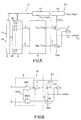
- Fig. 5 shows a semiconductor memory device according to an embodiment of the present invention, wherein a data output circuit portion in particular is shown in detail.
- like elements to those shown in Fig. 1 are represented by using identical reference numerals.
- CMOS complementary metal-oxide-semiconductor
- the memory cell array 4, output control circuit 3, and associated circuits are powered with a power source P1 dedicated to the internal circuit.
- the transistors T0, T1, and T2 are powered with another power source P2 dedicated to the output circuit.
- the output control circuit 3 has the circuit arrangement, e.g., same as that shown in Fig. 2.
- data stored in the memory cell array 4 is read via the output control circuit 3.
- the read-out data controls the gates of the transistors T1 and T0 to output the data from the data output terminal D out .
- the first node 1 of the output control circuit 3 therefore takes the same potential as at the data output terminal D out .
- the data output terminal D out is made to have the same potential as the ground potential V ss1 of the power source P1 dedicated to the internal circuit.
- noises at the ground potential V ss1 of the power source P1 dedicated to the internal circuit generate as shown in Fig. 4(c) when "0" is outputted from the data output terminal D out . Even if the noises are in synchronism with noises at the power source P2 dedicated to the output circuit, data can be correctly read because the transistor T2 is turned on.
- Fig. 6 shows the second embodiment of the present invention.
- an output circuit 20 is provided with C-MOS transistors T10 including a P-channel transistor T3 and an N-channel transistor T4.
- An output of an AND gate I is applied via an inverter IV to the gate of the P-channel transistor T3.
- the transistor T2 causes the ground potentials V ss1 and V ss2 of the plurality of power sources to take the same potential, when a data having the same level as the ground potential V ss2 is outputted. Accordingly, output noises can be suppressed while improving the reliability of output data.
- the present invention in a device having independent power sources respectively dedicated to supply power to an internal circuit such as a memory cell array and to an output circuit for externally outputting the data read from the memory cell, if a data output to the external takes a ground potential of the power source dedicated to the output circuit, the ground potentials of the two independent power sources are made equal. Therefore, even a data at the ground potential is to be outputted from the output circuit, the data can be correctly outputted without any influence of noises, thereby improving the reliability of the device.
Landscapes
- Engineering & Computer Science (AREA)
- Power Engineering (AREA)
- Microelectronics & Electronic Packaging (AREA)
- Computer Hardware Design (AREA)
- Static Random-Access Memory (AREA)
- Dram (AREA)
- Electronic Switches (AREA)
- Logic Circuits (AREA)
Claims (9)
- Halbleiterspeichereinrichtung, umfassend:eine erste Energiequelle (P1), die einen Anschluß mit einem ersten Nicht-Massepotential (Vcc1) und einen Anschluß mit einem ersten Massepotential (Vss1) aufweist;eine interne Schaltung (10), die Energie von der ersten Energiequelle (P1) erhält, wobei die interne Schaltung eine Speicherzelle (MC) eines Speicherzellenfelds (4) gemäß einer eingegebenen Adresse (A1, A2) wählt und einen ersten Ausgabeanschluß (1) und einen zweiten Ausgabeanschluß (2) aufweist, und wobei der erste Ausgabeanschluß eines der Potentiale (Vcc1) und (Vss1) der Potentialanschlüsse ausgibt und wobei der andere Ausgabeanschluß das andere der Potentiale der Potentialanschlüsse ausgibt, gemäß dem Datenwert in der gespeicherten Speicherzelle; undeine Ausgabeschaltung;gekennzeichnet durcheine zweite Energiequelle (P2), die einen Anschluß mit einem zweiten Nicht-Massepotential (Vcc2) und einenAnschluß mit einem zweiten Massepotential (Vss2) aufweist; undwobei die Ausgabeschaltung Energie von der zweiten Energiequelle erhält, wobei die Ausgabeschaltung eine erste und eine zweite Schalteinrichtung (T1, T0; T3, T4) aufweist, die zwischen den Anschluß mit dem zweiten Nicht-Massepotential (Vcc2) und den Anschluß mit dem zweiten Massepotential (Vss2) in Reihe geschaltet sind, wobei die Steueranschlüsse der ersten und zweiten Schalteinrichtungen mit den ersten und zweiten Ausgabeanschlüssen (1, 2) verbunden sind und mit einer dritten Schalteinrichtung (T2), die zwischen eine Verbindung zwischen der ersten und zweiten Schalteinrichtung, die mit dem Datenausgabeanschluß (Dout) verbunden ist, von dem ein Datenwert extern ausgegeben wird, und den ersten Ausgabeanschluß geschaltet ist, und wobei der Steueranschluß der dritten Schalteinrichtung mit dem zweiten Ausgabeanschluß (2) verbunden ist.
- Einrichtung nach Anspruch 1, dadurch gekennzeichnet, daß die erste und zweite Schalteinrichtung (T1, T0) jeweils Schaltelemente des gleichen Leitfähigkeitstyps sind und die Steueranschlüsse der ersten und zweiten Schalteinrichtungen direkt mit den ersten und zweiten Ausgabeanschlüssen (1, 2) verbunden sind.
- Einrichtung nach Anspruch 2, dadurch gekennzeichnet, daß die erste und zweite Schalteinrichtung (T1, T0) N-Kanal-Transistoren sind.
- Einrichtung nach Anspruch 3, dadurch gekennzeichnet, daß die dritte Schalteinrichtung (T2) ein N-Kanal-Transistor ist.
- Einrichtung nach Anspruch 1, dadurch gekennzeichnet, daß die interne Schaltung eine Ausgabesteuerschaltung (3) umfaßt, die einen Eingangsanschluß zum Empfangen eines Datenwerts von der gewählten Speicherzelle (MC) und die ersten und zweiten Ausgabeanschlüsse (1, 2) aufweist.
- Einrichtung nach Anspruch 5, dadurch gekennzeichnet, daß die Ausgabesteuerschaltung (3) eine logische Operation zwischen einem Aktivierungssignal (ENBL) und einem Datenwert von der gewählten Speicherzelle (MC) ausführt, um den Datenwert an die ersten und zweiten Ausgabeanschlüsse auszugeben.
- Einrichtung nach Anspruch 1, dadurch gekennzeichnet, daß die erste und zweite Schalteinrichtung (T3, T4) CMOS-Transistoren (T10) umfassen, wobei der Steueranschluß der ersten Schalteinrichtung (T3) und der erste Ausgabeanschluß (1) über einen Inverter zusammengeschaltet sind, und der Steueranschluß der zweiten Schalteinrichtung (T4) direkt mit dem zweiten Ausgabeanschluß (2) verbunden ist.
- Einrichtung nach Anspruch 7, dadurch gekennzeichnet, daß die erste und zweite Schalteinrichtung (T3, T4) P- und N-Kanal-Transistoren sind.
- Einrichtung nach Anspruch 8, dadurch gekennzeichnet, daß die dritte Schalteinrichtung (T2) ein N-Kanal-Transistor ist.
Applications Claiming Priority (2)
| Application Number | Priority Date | Filing Date | Title |
|---|---|---|---|
| JP2164677A JPH0834060B2 (ja) | 1990-06-22 | 1990-06-22 | 半導体記憶装置 |
| JP164677/90 | 1990-06-22 |
Publications (3)
| Publication Number | Publication Date |
|---|---|
| EP0464468A2 EP0464468A2 (de) | 1992-01-08 |
| EP0464468A3 EP0464468A3 (en) | 1993-03-31 |
| EP0464468B1 true EP0464468B1 (de) | 1996-09-04 |
Family
ID=15797747
Family Applications (1)
| Application Number | Title | Priority Date | Filing Date |
|---|---|---|---|
| EP91110045A Expired - Lifetime EP0464468B1 (de) | 1990-06-22 | 1991-06-19 | Halbleiterspeicheranordnung |
Country Status (5)
| Country | Link |
|---|---|
| US (1) | US5287306A (de) |
| EP (1) | EP0464468B1 (de) |
| JP (1) | JPH0834060B2 (de) |
| KR (1) | KR950001128B1 (de) |
| DE (1) | DE69121804T2 (de) |
Families Citing this family (5)
| Publication number | Priority date | Publication date | Assignee | Title |
|---|---|---|---|---|
| US5546036A (en) * | 1992-08-27 | 1996-08-13 | Siemens Aktiengesellschaft | Circuit array for amplifying and holding data with different supply |
| EP0584390B1 (de) * | 1992-08-27 | 1998-07-08 | Siemens Aktiengesellschaft | Schaltungsanordnung zum Verstärken und Halten von Daten mit verschiedenen Versorgungsspannungen |
| US5440258A (en) * | 1994-02-08 | 1995-08-08 | International Business Machines Corporation | Off-chip driver with voltage regulated predrive |
| KR100211758B1 (ko) * | 1995-08-18 | 1999-08-02 | 윤종용 | 멀티 파워를 사용하는 데이터 출력버퍼 |
| US7639540B2 (en) * | 2007-02-16 | 2009-12-29 | Mosaid Technologies Incorporated | Non-volatile semiconductor memory having multiple external power supplies |
Family Cites Families (4)
| Publication number | Priority date | Publication date | Assignee | Title |
|---|---|---|---|---|
| JPS60115092A (ja) * | 1983-11-28 | 1985-06-21 | Nec Corp | 半導体記憶回路 |
| JP2573320B2 (ja) * | 1988-07-11 | 1997-01-22 | 株式会社東芝 | 出力バッファ回路 |
| JPH0344890A (ja) * | 1989-07-12 | 1991-02-26 | Toshiba Corp | 半導体記憶装置のデータ出力制御回路 |
| JPH0646514B2 (ja) * | 1989-10-19 | 1994-06-15 | 株式会社東芝 | 半導体装置 |
-
1990
- 1990-06-22 JP JP2164677A patent/JPH0834060B2/ja not_active Expired - Fee Related
-
1991
- 1991-06-19 EP EP91110045A patent/EP0464468B1/de not_active Expired - Lifetime
- 1991-06-19 DE DE69121804T patent/DE69121804T2/de not_active Expired - Fee Related
- 1991-06-20 US US07/718,449 patent/US5287306A/en not_active Expired - Lifetime
- 1991-06-21 KR KR1019910010266A patent/KR950001128B1/ko not_active Expired - Fee Related
Also Published As
| Publication number | Publication date |
|---|---|
| JPH0834060B2 (ja) | 1996-03-29 |
| JPH0457288A (ja) | 1992-02-25 |
| EP0464468A2 (de) | 1992-01-08 |
| EP0464468A3 (en) | 1993-03-31 |
| KR950001128B1 (ko) | 1995-02-11 |
| US5287306A (en) | 1994-02-15 |
| DE69121804T2 (de) | 1997-02-13 |
| KR920001521A (ko) | 1992-01-30 |
| DE69121804D1 (de) | 1996-10-10 |
Similar Documents
| Publication | Publication Date | Title |
|---|---|---|
| US4114049A (en) | Counter provided with complementary field effect transistor inverters | |
| US6133752A (en) | Semiconductor integrated circuit having tri-state logic gate circuit | |
| KR100272163B1 (ko) | 대기용어레이전압발생기를갖는반도체메모리장치 | |
| US5400295A (en) | Semiconductor integrated circuit device and semiconductor memory device | |
| EP0254474A1 (de) | Programmierbares CMOS-Logik-Array | |
| KR910003598B1 (ko) | 독립의 전류통로에 접속된 데이터출력버퍼회로를 갖춘 반도체집적회로 | |
| JPS61283092A (ja) | リセツトあるいはセツト付記憶回路を有した半導体集積回路 | |
| JPS62100021A (ja) | バイポ−ラ−fetインタ−フエイス回路 | |
| KR100203208B1 (ko) | 반도체 메모리 장치 | |
| EP0464468B1 (de) | Halbleiterspeicheranordnung | |
| US5786719A (en) | Mode setting circuit and mode setting apparatus used to select a particular semiconductor function | |
| JP2000164813A (ja) | 半導体集積回路 | |
| CA1037605A (en) | Driver cell with memory and shift capability | |
| US6239639B1 (en) | Latch circuit | |
| KR930011433A (ko) | 반도체 집적회로장치 | |
| US5293515A (en) | Amplifier circuit having two inverters | |
| US6172527B1 (en) | Output circuit capable of reducing feedthrough current | |
| JPS63316917A (ja) | 集積半導体回路内の発生器回路 | |
| EP0821484A1 (de) | Hohen Spannungen widerstehende Ausgangsstufe | |
| US5514993A (en) | Apparatus for preventing transferring noise of digital signal | |
| EP0417973A2 (de) | Verstärkerschaltung mit zwei Invertern | |
| KR960001858B1 (ko) | 반도체 메모리 장치의 데이타 출력 구동 회로 | |
| KR100255701B1 (ko) | 한 비트를 래칭하기 위한 회로와 이를 어드레스 래치로 이용하는 방법 | |
| JP3066645B2 (ja) | 半導体装置 | |
| JPH02283123A (ja) | 半導体装置 |
Legal Events
| Date | Code | Title | Description |
|---|---|---|---|
| PUAI | Public reference made under article 153(3) epc to a published international application that has entered the european phase |
Free format text: ORIGINAL CODE: 0009012 |
|
| 17P | Request for examination filed |
Effective date: 19910619 |
|
| AK | Designated contracting states |
Kind code of ref document: A2 Designated state(s): DE FR GB |
|
| PUAL | Search report despatched |
Free format text: ORIGINAL CODE: 0009013 |
|
| AK | Designated contracting states |
Kind code of ref document: A3 Designated state(s): DE FR GB |
|
| 17Q | First examination report despatched |
Effective date: 19950830 |
|
| GRAH | Despatch of communication of intention to grant a patent |
Free format text: ORIGINAL CODE: EPIDOS IGRA |
|
| GRAA | (expected) grant |
Free format text: ORIGINAL CODE: 0009210 |
|
| GRAH | Despatch of communication of intention to grant a patent |
Free format text: ORIGINAL CODE: EPIDOS IGRA |
|
| AK | Designated contracting states |
Kind code of ref document: B1 Designated state(s): DE FR GB |
|
| REF | Corresponds to: |
Ref document number: 69121804 Country of ref document: DE Date of ref document: 19961010 |
|
| ET | Fr: translation filed | ||
| PGFP | Annual fee paid to national office [announced via postgrant information from national office to epo] |
Ref country code: FR Payment date: 19970610 Year of fee payment: 7 |
|
| PGFP | Annual fee paid to national office [announced via postgrant information from national office to epo] |
Ref country code: DE Payment date: 19970630 Year of fee payment: 7 |
|
| PLBE | No opposition filed within time limit |
Free format text: ORIGINAL CODE: 0009261 |
|
| STAA | Information on the status of an ep patent application or granted ep patent |
Free format text: STATUS: NO OPPOSITION FILED WITHIN TIME LIMIT |
|
| 26N | No opposition filed | ||
| REG | Reference to a national code |
Ref country code: GB Ref legal event code: 746 Effective date: 19981010 |
|
| PG25 | Lapsed in a contracting state [announced via postgrant information from national office to epo] |
Ref country code: FR Free format text: LAPSE BECAUSE OF NON-PAYMENT OF DUE FEES Effective date: 19990226 |
|
| PG25 | Lapsed in a contracting state [announced via postgrant information from national office to epo] |
Ref country code: DE Free format text: LAPSE BECAUSE OF NON-PAYMENT OF DUE FEES Effective date: 19990401 |
|
| REG | Reference to a national code |
Ref country code: FR Ref legal event code: ST |
|
| REG | Reference to a national code |
Ref country code: GB Ref legal event code: IF02 |
|
| PGFP | Annual fee paid to national office [announced via postgrant information from national office to epo] |
Ref country code: GB Payment date: 20060614 Year of fee payment: 16 |
|
| GBPC | Gb: european patent ceased through non-payment of renewal fee |
Effective date: 20070619 |
|
| PG25 | Lapsed in a contracting state [announced via postgrant information from national office to epo] |
Ref country code: GB Free format text: LAPSE BECAUSE OF NON-PAYMENT OF DUE FEES Effective date: 20070619 |