EP0463682A1 - Circuit de verrouillage - Google Patents
Circuit de verrouillage Download PDFInfo
- Publication number
- EP0463682A1 EP0463682A1 EP91201525A EP91201525A EP0463682A1 EP 0463682 A1 EP0463682 A1 EP 0463682A1 EP 91201525 A EP91201525 A EP 91201525A EP 91201525 A EP91201525 A EP 91201525A EP 0463682 A1 EP0463682 A1 EP 0463682A1
- Authority
- EP
- European Patent Office
- Prior art keywords
- transistors
- main
- electrodes
- junction
- transistor
- Prior art date
- Legal status (The legal status is an assumption and is not a legal conclusion. Google has not performed a legal analysis and makes no representation as to the accuracy of the status listed.)
- Granted
Links
- 230000008878 coupling Effects 0.000 claims description 2
- 238000010168 coupling process Methods 0.000 claims description 2
- 238000005859 coupling reaction Methods 0.000 claims description 2
- 230000000717 retained effect Effects 0.000 abstract 1
- 230000000295 complement effect Effects 0.000 description 6
- 230000003111 delayed effect Effects 0.000 description 3
- 230000001960 triggered effect Effects 0.000 description 3
- 230000000694 effects Effects 0.000 description 2
- 230000003071 parasitic effect Effects 0.000 description 2
- 230000009977 dual effect Effects 0.000 description 1
Images


Classifications
-
- H—ELECTRICITY
- H03—ELECTRONIC CIRCUITRY
- H03K—PULSE TECHNIQUE
- H03K3/00—Circuits for generating electric pulses; Monostable, bistable or multistable circuits
- H03K3/02—Generators characterised by the type of circuit or by the means used for producing pulses
- H03K3/353—Generators characterised by the type of circuit or by the means used for producing pulses by the use, as active elements, of field-effect transistors with internal or external positive feedback
- H03K3/356—Bistable circuits
- H03K3/356017—Bistable circuits using additional transistors in the input circuit
- H03K3/356034—Bistable circuits using additional transistors in the input circuit the input circuit having a differential configuration
Definitions
- the invention relates to a latch circuit comprising:
- the first main electrode, the second main electrode and the control electrode of a transistor correspond to the emitter, collector and base respectively, when bipolar transistors are used and to the source, drain and gate respectively, when unipolar transistors are used.
- a latch circuit of this type is known from "An 8- bit 100-MHz Full-Nyquist Analog-to-Digital Converter", IEEE Journal Of Solid-State Circuits, Vol. 23, No. 6, December 1988, pp. 1334-1344, Fig. 12.
- the transistors are of the bipolar NPN type. If the clock signal is high, the fifth and sixth transistors of the switching means are rendered conductive and connect the collectors of the first and second transistors of the differential amplifier to the first and second load impedances. An amplified data signal is then present on the first and second output terminals. At that moment the flip-flop is not active because the second junction is maintained currentless by means of two further transistors whose bases are biased by means of the inverse clock signal.
- the latch circuit comprises two further transistors whose collectors are connected to the second junction, the bases to an input terminal for receiving an inverted clock signal and whose emitters, in a first or second emitter junction respectively, are connected to the emitter of the fifth or sixth transistor respectively. Concurrently with the drop of the clock signal, the two further transistors are rendered conductive by the inverted clock signal so that the second junction is connected to the collectors of the first and second transistors of the differential amplifier.
- the bias current of the biasing means now flows through the first and second transistors to the second junction so that the flip-flop is triggered again and the differential voltage across the first and second output terminals is amplified and latched regeneratively.
- a disadvantage of this prior-art latch circuit is that the first or second emitter junction may become currentless for a longer period of time if the sign of the differential voltage on the data signal input terminals is not inverted. During that period of time the voltage on the emitter junction concerned may flow away. If, subsequently, the sign of the differential voltage is inverted, the relevant transistor of the differential amplifier will become conductive and supply current to the emitter junction. As a result of the presence of parasitic capacitances in the emitter junction it will take some time before the capacitances are charged and the differential voltage across the first and second output terminals is brought into agreement with the sign inversion of the data signal.
- a latch circuit of the type mentioned in the preamble is characterized according to the invention in that the second junction is coupled to the second main electrode of the second transistor and in that the flip-flop further includes seventh and eighth transistors having each a first and a second main electrode and a control electrode, the first main electrodes being coupled to each other and to the second main electrode of the first transistor in a third junction, and the control electrodes and the second main electrodes of the seventh and eighth transistors being connected to corresponding electrodes of the respective third and fourth transistors.
- the flip-flop comprises two additional transistors of which, again assuming they are bipolar NPN transistors, the emitters are connected to the collector of the first transistor of the differential amplifier in a third junction, whereas the second junction is connected to the collector of the second transistor. If the clock signal at the clock signal input and the data signal at the data signal terminal connected to the base of the first transistor are both high, the first and fifth transistors will be conductive and the voltage in the third junction will be fixed at a single diode voltage when a clock signal voltage is applied. With a sufficiently large data signal the second transistor will block and it will be possible for the voltage in the second junction to flow away in positive direction.
- the voltage in the second junction will be fixed through the sixth transistor if the clock signal voltage is high and through the third and fourth transistors of the flip-flop and the first and second load impedances if the clock signal voltage is low.
- the most critical situation is the one in which the data signal on the base of the first transistor presents a variation from strongly positive to just below zero just before the decision moment, that is to say, right before the clock signal becomes low. The latching could then take place right before the zero crossing is detected across the first and second output terminals. If the sixth transistor has not been triggered properly because the second junction has not yet been fully charged, also the start of the latching operation will be slightly delayed for lack of current so that still the right decision will be made.
- the latch circuit according to the invention is furthermore advantageous in that the number of stacked transistors is reduced by one, so that it will be possible to work with a smaller supply voltage or with larger signals.
- the delay from the data signal input terminals to the output terminals is shorter due to the smaller number of transistors in the signal path between these terminals.
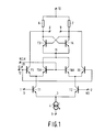
- Fig. 1 shows a prior-art latch circuit.
- a complementary data signal D, ND to be latched is applied to data signal input terminals 1, 2 which are connected to the bases of the transistors T1, T2 respectively, whose emitters are interconnected in junction 3.
- the junction 3 is connected to a negative supply terminal 5 through a bias current source 4.
- the collectors of the transistors T1 and T2 are connected over the emitter-collector path of the transistors T5 and T6 respectively, to load impedances 6 and 7 respectively, arranged as resistors in this circuit.
- the junction of the collector of transistor T5 and the load impedance 6 is connected to a first output terminal 8, whereas the junction of the collector of transistor T6 and load impedance 7 is connected to a second output terminal 9.
- the two remaining connecting points of the load impedances 6 and 7 are connected to a positive supply terminal 10.
- the output terminals 8 and 9 are further connected to the transistors T3 and T4 arranged as flip-flops.
- the base of transistor T4 and the collector of transistor T3 are connected to output terminal 8 and the base of transistor T3 and the collector of transistor T4 are connected to output terminal 9.
- the emitters of the transistors T3 and T4 are interconnected in a second junction 11 which is connected over the collector-emitter paths of two further transistors T5A and T6A to the collectors of the transistors T1 and T2 respectively.
- the bases of the transistors T5 and T6 are both connected to a clock signal input 12 to which a clock signal CLK is applied.
- the bases of the further transistors T5A and T6A are both connected to the clock signal input 13 to which a complementary clock signal NCLK is applied.
- the transistors T5 and T6 will be conductive and the transistors T5A and T6A will block.
- the collectors of the transistors T1 and T2 are now connected to the load impedances 6 and 7 so that an amplified data signal is generated across the output terminals 8, 9.
- Junction 11 of the flip-flop is currentless so that the flip-flop is not active.
- the flip-flop If the clock signal CLK is low and the complementary clock signal NCLK high, the transistors T5 and T6 will block and the transistors T5A and T6A will be conductive. In that case the flip-flop is active because the junction 11 is connected to the bias current source 4 through the transistors T5A, T1 and the transistors T6A, T2. The flip-flop now regenerates and latches the voltage difference across the output terminals 8 and 9. Fluctuations in the data signal D, ND do not have any effect on the latching because these fluctuations do not change the sum of the current through junction 11.
- the junction 11 of the flip-flop will be currentless if the clock signal CLK is high.
- the voltage in this junction 11 may therefore flow away to unspecified higher values so that the next latching operation of the flip-flop in which there is just a sign inversion of the input data signal, may present an inaccuracy.
- This inaccuracy is caused by the fact that the recharging of the parasitic capacitances which act on the junction 11 presents a slowness due to which the sign inversion is transferred to the voltages on the load resistances in a delayed manner and may be too late for the next decision moment. Inaccuracy augments with smaller input data signals and higher clock signal frequencies.
- Fig. 2 shows an embodiment of a latch circuit according to the invention comprising bipolar NPN transistors.
- like components have like reference numerals as shown in Fig. 1.
- the further transistors T5A and T6A are omitted and so is the complementary clock signal input 13.
- the collector of transistor T2 is now connected directly to the second junction 11 of flip-flops T3, T4 whereas the flip-flop is extended by the transistors T7 and T8 whose bases and collectors are connected to the corresponding electrodes of the respective transistors T3 and T4 and whose emitters are connected to each other and to the collector of transistor T1 in a third junction 14.
- the bases of the transistors T3, T4 and of the transistors T7, T8 are not connected directly to the output terminals 9, 8 respectively, as was the case in Fig. 1, but through the base-emitter junction of buffer transistors T10 and T9 respectively.
- the collectors of these transistors T9 and T10 are coupled to the positive supply terminal 10 and their emitters are connected to the negative supply terminal 5 through appropriate load impedances arranged as a series combination of two transistors T11, T12 and T13, T14 respectively, arranged as diodes and through bias current sources 15, 16 respectively.
- the transistors arranged as diodes act as level shifters.
- the junctions between the current sources 15, 16 and the diodes T11, T12 and T13, T14 respectively, are connected to output terminals 17 and 18 from which buffered complementary output signals can be tapped.
- the transistors T5 and T6 will be conductive so that the collectors of the transistors T1 and T2 are connected to the load impedances 6 and 7.
- the data signals D, ND on the terminals 1,2 appear as amplified versions on the output terminals 8 and 9.
- the emitters of the transistors T5, T6 respectively are connected directly to the emitters of the corresponding flip-flops T7, T8 and T3, T4 respectively, so that in the most critical situation in which the input data signal has just had sign inversion when the clock becomes high, a slowness during the recharging of the junctions 14, 11 respectively will cause a delay in applying the correct differential voltage to the load impedances 6 and 7.
- the flip-flop will also be triggered in a delayed manner so that still the right decision is made. If the clock signal CLK is low, the transistors T5 and T6 will block. The voltage difference across the output terminals 8 and 9 will now be latched by the flip-flop T3, T7, T4, T8. The bias current of current source 4 will be distributed over the transistors T1 and T2 as a result of any data signal variations on the terminals 1 and 2. However, since the flip-flop has a dual arrangement in the transistors T7 and T8, this does not affect the currents through the load impedances 6 and 7, so that the latched operation of the flip-flop is not disturbed by any data signal variations.
- Fig. 3 represents a second embodiment of a latch circuit comprising unipolar N-channel MOS transistors.
- the circuit is furthermore identical with that of Fig. 2 and like components have like reference characters.
- the invention is not restricted to the exemplary embodiments shown in Figs. 2 and 3.
- the load impedances 6 and 7 may also be constituted by a series combination of transistors arranged as diodes.
- the buffer transistors T9, T10 with associated load impedances T11, T12, 15 and T13, T14, 16 respectively, may also be omitted. In that case the bases of the transistors T3, T7 and of the transistors T4, T8 are to be connected directly to the output terminals 9, 8 respectively.
- resistors may be selected.
- the bipolar NPN transistors may be replaced by bipolar PNP transistors and the unipolar N-channel transistors by unipolar P-channel transistors, whereas the supply voltage on the supply terminals 5 and 10 is then to be reversed.
- the circuit may partially comprise unipolar transistors, for example, the transistors T1 and T2 and partially comprise bipolar transistors, for example the transistors T3, T4.
Landscapes
- Manipulation Of Pulses (AREA)
- Logic Circuits (AREA)
Applications Claiming Priority (2)
| Application Number | Priority Date | Filing Date | Title |
|---|---|---|---|
| NL9001442A NL9001442A (nl) | 1990-06-22 | 1990-06-22 | Vergrendelschakeling. |
| NL9001442 | 1990-06-22 |
Publications (2)
| Publication Number | Publication Date |
|---|---|
| EP0463682A1 true EP0463682A1 (fr) | 1992-01-02 |
| EP0463682B1 EP0463682B1 (fr) | 1996-03-27 |
Family
ID=19857307
Family Applications (1)
| Application Number | Title | Priority Date | Filing Date |
|---|---|---|---|
| EP91201525A Expired - Lifetime EP0463682B1 (fr) | 1990-06-22 | 1991-06-18 | Circuit de verrouillage |
Country Status (5)
| Country | Link |
|---|---|
| US (1) | US5103117A (fr) |
| EP (1) | EP0463682B1 (fr) |
| JP (1) | JP3137680B2 (fr) |
| DE (1) | DE69118249T2 (fr) |
| NL (1) | NL9001442A (fr) |
Families Citing this family (6)
| Publication number | Priority date | Publication date | Assignee | Title |
|---|---|---|---|---|
| US5311086A (en) * | 1991-03-01 | 1994-05-10 | Kabushiki Kaisha Toshiba | Multiplying circuit with improved linearity and reduced leakage |
| US5343428A (en) * | 1992-10-05 | 1994-08-30 | Motorola Inc. | Memory having a latching BICMOS sense amplifier |
| US5430336A (en) * | 1992-10-23 | 1995-07-04 | Sony Corporation | Emitter coupled logic circuit |
| JP2570575B2 (ja) * | 1993-06-17 | 1997-01-08 | 日本電気株式会社 | フリップフロップ回路 |
| US7009438B2 (en) * | 1999-10-08 | 2006-03-07 | Lucent Technologies Inc. | Trans-admittance trans-impedance logic for integrated circuits |
| WO2008114380A1 (fr) * | 2007-03-19 | 2008-09-25 | Fujitsu Limited | Circuit de stockage et procédé de stockage |
Citations (3)
| Publication number | Priority date | Publication date | Assignee | Title |
|---|---|---|---|---|
| EP0013686A1 (fr) * | 1978-12-26 | 1980-08-06 | International Business Machines Corporation | Bascule à verrouillage |
| EP0130646A1 (fr) * | 1983-06-29 | 1985-01-09 | Laboratoires D'electronique Et De Physique Appliquee L.E.P. | Comparateur synchronisé |
| US4542308A (en) * | 1982-12-23 | 1985-09-17 | Advanced Micro Devices, Inc. | Sampling comparator circuit for processing a differential input |
Family Cites Families (2)
| Publication number | Priority date | Publication date | Assignee | Title |
|---|---|---|---|---|
| JPS5329057A (en) * | 1976-08-30 | 1978-03-17 | Nec Corp | Master slave type flip flop circuit |
| FR2581811A1 (fr) * | 1985-05-10 | 1986-11-14 | Radiotechnique Compelec | Module multiplexeur numerique a n entrees et multiplexeur a n2 entrees incorporant de tels modules |
-
1990
- 1990-06-22 NL NL9001442A patent/NL9001442A/nl unknown
-
1991
- 1991-06-10 US US07/713,184 patent/US5103117A/en not_active Expired - Fee Related
- 1991-06-18 DE DE69118249T patent/DE69118249T2/de not_active Expired - Fee Related
- 1991-06-18 EP EP91201525A patent/EP0463682B1/fr not_active Expired - Lifetime
- 1991-06-21 JP JP03175806A patent/JP3137680B2/ja not_active Expired - Fee Related
Patent Citations (3)
| Publication number | Priority date | Publication date | Assignee | Title |
|---|---|---|---|---|
| EP0013686A1 (fr) * | 1978-12-26 | 1980-08-06 | International Business Machines Corporation | Bascule à verrouillage |
| US4542308A (en) * | 1982-12-23 | 1985-09-17 | Advanced Micro Devices, Inc. | Sampling comparator circuit for processing a differential input |
| EP0130646A1 (fr) * | 1983-06-29 | 1985-01-09 | Laboratoires D'electronique Et De Physique Appliquee L.E.P. | Comparateur synchronisé |
Also Published As
| Publication number | Publication date |
|---|---|
| US5103117A (en) | 1992-04-07 |
| JPH04233316A (ja) | 1992-08-21 |
| DE69118249D1 (de) | 1996-05-02 |
| EP0463682B1 (fr) | 1996-03-27 |
| DE69118249T2 (de) | 1996-10-02 |
| NL9001442A (nl) | 1992-01-16 |
| JP3137680B2 (ja) | 2001-02-26 |
Similar Documents
| Publication | Publication Date | Title |
|---|---|---|
| US4885484A (en) | Voltage clamped differential to single ended converter circuit | |
| US4783604A (en) | Buffer circuit for outputting signals of different polarities | |
| CA1235504A (fr) | Element de stockage de donnees a portes d'entree et de sortie isolees d'un circuit a regeneration | |
| US4517476A (en) | ECL Gate having emitter bias current switched by input signal | |
| JP2852971B2 (ja) | Ttlからecl/cmlへの変換回路 | |
| US5359241A (en) | ECL circuit | |
| US5206546A (en) | Logic circuit including variable impedance means | |
| EP0463682B1 (fr) | Circuit de verrouillage | |
| EP0131205B1 (fr) | Générateur de potentiel de commande de source de courant pour de circuits de logique CML | |
| US5146116A (en) | Ecl circuit with a reduced power active pulldown | |
| US4602172A (en) | High input impedance circuit | |
| EP0119644A1 (fr) | Convertisseur d'impédance en forme d'amplificateur de tampon | |
| EP0316884A2 (fr) | Circuit déclencheur de Schmitt | |
| JPH1197774A (ja) | 出力回路装置 | |
| US4418321A (en) | Feedback amplifier or threshold value switch for a current feed differential stage | |
| WO1985001164A1 (fr) | Bascule ttl | |
| EP0127858A1 (fr) | Bascule ayant une remise à zéro synchrone | |
| EP0432472A2 (fr) | Circuit CMOS comportant des transistors bipolaires dans l'étage de sortie | |
| JPS60254905A (ja) | バイポーラ増幅器回路 | |
| JP3980337B2 (ja) | トラックホールド回路 | |
| JPS59500078A (ja) | デ−タラツチ用リセツト回路 | |
| US3300654A (en) | Schmitt trigger with active collector to base coupling | |
| EP0750393A2 (fr) | Un étage de sortie d'un amplificateur opérationnel haute tension | |
| EP0520830A2 (fr) | Dispositif et méthode pour la conversion d'un signal de type ECL en un signal CMOS | |
| US20050218951A1 (en) | Flip-flop circuit and frequency division circuit using same |
Legal Events
| Date | Code | Title | Description |
|---|---|---|---|
| PUAI | Public reference made under article 153(3) epc to a published international application that has entered the european phase |
Free format text: ORIGINAL CODE: 0009012 |
|
| AK | Designated contracting states |
Kind code of ref document: A1 Designated state(s): DE FR GB IT |
|
| 17P | Request for examination filed |
Effective date: 19920702 |
|
| 17Q | First examination report despatched |
Effective date: 19950515 |
|
| GRAH | Despatch of communication of intention to grant a patent |
Free format text: ORIGINAL CODE: EPIDOS IGRA |
|
| GRAA | (expected) grant |
Free format text: ORIGINAL CODE: 0009210 |
|
| AK | Designated contracting states |
Kind code of ref document: B1 Designated state(s): DE FR GB IT |
|
| REF | Corresponds to: |
Ref document number: 69118249 Country of ref document: DE Date of ref document: 19960502 |
|
| ITF | It: translation for a ep patent filed | ||
| ET | Fr: translation filed | ||
| PLBE | No opposition filed within time limit |
Free format text: ORIGINAL CODE: 0009261 |
|
| STAA | Information on the status of an ep patent application or granted ep patent |
Free format text: STATUS: NO OPPOSITION FILED WITHIN TIME LIMIT |
|
| 26N | No opposition filed | ||
| REG | Reference to a national code |
Ref country code: FR Ref legal event code: CD |
|
| PGFP | Annual fee paid to national office [announced via postgrant information from national office to epo] |
Ref country code: FR Payment date: 20010625 Year of fee payment: 11 |
|
| PGFP | Annual fee paid to national office [announced via postgrant information from national office to epo] |
Ref country code: GB Payment date: 20010629 Year of fee payment: 11 |
|
| PGFP | Annual fee paid to national office [announced via postgrant information from national office to epo] |
Ref country code: DE Payment date: 20010821 Year of fee payment: 11 |
|
| REG | Reference to a national code |
Ref country code: GB Ref legal event code: IF02 |
|
| PG25 | Lapsed in a contracting state [announced via postgrant information from national office to epo] |
Ref country code: GB Free format text: LAPSE BECAUSE OF NON-PAYMENT OF DUE FEES Effective date: 20020618 |
|
| PG25 | Lapsed in a contracting state [announced via postgrant information from national office to epo] |
Ref country code: DE Free format text: LAPSE BECAUSE OF NON-PAYMENT OF DUE FEES Effective date: 20030101 |
|
| GBPC | Gb: european patent ceased through non-payment of renewal fee |
Effective date: 20020618 |
|
| PG25 | Lapsed in a contracting state [announced via postgrant information from national office to epo] |
Ref country code: FR Free format text: LAPSE BECAUSE OF NON-PAYMENT OF DUE FEES Effective date: 20030228 |
|
| REG | Reference to a national code |
Ref country code: FR Ref legal event code: ST |
|
| PG25 | Lapsed in a contracting state [announced via postgrant information from national office to epo] |
Ref country code: IT Free format text: LAPSE BECAUSE OF NON-PAYMENT OF DUE FEES;WARNING: LAPSES OF ITALIAN PATENTS WITH EFFECTIVE DATE BEFORE 2007 MAY HAVE OCCURRED AT ANY TIME BEFORE 2007. THE CORRECT EFFECTIVE DATE MAY BE DIFFERENT FROM THE ONE RECORDED. Effective date: 20050618 |