EP0457737A2 - MOS/BIP-Schutzschaltung - Google Patents
MOS/BIP-Schutzschaltung Download PDFInfo
- Publication number
- EP0457737A2 EP0457737A2 EP91830206A EP91830206A EP0457737A2 EP 0457737 A2 EP0457737 A2 EP 0457737A2 EP 91830206 A EP91830206 A EP 91830206A EP 91830206 A EP91830206 A EP 91830206A EP 0457737 A2 EP0457737 A2 EP 0457737A2
- Authority
- EP
- European Patent Office
- Prior art keywords
- node
- bipolar transistor
- enabling
- collector
- coupled
- Prior art date
- Legal status (The legal status is an assumption and is not a legal conclusion. Google has not performed a legal analysis and makes no representation as to the accuracy of the status listed.)
- Granted
Links
Images

Classifications
-
- H—ELECTRICITY
- H10—SEMICONDUCTOR DEVICES; ELECTRIC SOLID-STATE DEVICES NOT OTHERWISE PROVIDED FOR
- H10D—INORGANIC ELECTRIC SEMICONDUCTOR DEVICES
- H10D89/00—Aspects of integrated devices not covered by groups H10D84/00 - H10D88/00
- H10D89/60—Integrated devices comprising arrangements for electrical or thermal protection, e.g. protection circuits against electrostatic discharge [ESD]
- H10D89/601—Integrated devices comprising arrangements for electrical or thermal protection, e.g. protection circuits against electrostatic discharge [ESD] for devices having insulated gate electrodes, e.g. for IGFETs or IGBTs
- H10D89/711—Integrated devices comprising arrangements for electrical or thermal protection, e.g. protection circuits against electrostatic discharge [ESD] for devices having insulated gate electrodes, e.g. for IGFETs or IGBTs using bipolar transistors as protective elements
-
- H—ELECTRICITY
- H10—SEMICONDUCTOR DEVICES; ELECTRIC SOLID-STATE DEVICES NOT OTHERWISE PROVIDED FOR
- H10D—INORGANIC ELECTRIC SEMICONDUCTOR DEVICES
- H10D89/00—Aspects of integrated devices not covered by groups H10D84/00 - H10D88/00
- H10D89/60—Integrated devices comprising arrangements for electrical or thermal protection, e.g. protection circuits against electrostatic discharge [ESD]
- H10D89/601—Integrated devices comprising arrangements for electrical or thermal protection, e.g. protection circuits against electrostatic discharge [ESD] for devices having insulated gate electrodes, e.g. for IGFETs or IGBTs
- H10D89/811—Integrated devices comprising arrangements for electrical or thermal protection, e.g. protection circuits against electrostatic discharge [ESD] for devices having insulated gate electrodes, e.g. for IGFETs or IGBTs using FETs as protective elements
Definitions
- This invention concerns a bipolar protection circuit, manufactured according to CMOS technology and more particularly compatible with the conventional 2um CMOS process, and having I/V characteristic curves similar to those of conventional Zener devices.
- Zener diode As is known, there are many devices and circuits having supply voltages which should be maintained during operation within strictly defined limits regardless of the current flowing therethrough, and which therefore should be protected against over-voltage effects.
- a well-known device adapted to perform such a protection function is the Zener diode; in fact, its characteristic discharge voltage - the so-called Zener voltage - as a function of the current flowing therethrough is sufficiently constant to provide a satisfactory protection effect: in practice, its I/V characteristic curve has the well-known profile which is ideally vertical, practically very steep and effectively nearly vertical.
- CMOS integrated circuits namely CMOS integrated circuits having a built-in protection device.
- the principle upon which the circuit of this invention is based is to utilize the bipolar transistors that are always associated with the CMOS structures either as parasitic members (vertical transistors with collector materially coinciding with the substrate) or as implementable members (lateral transistors), if desired, in combination with a current MOS transistors.
- the circuit as proposed by this invention comprises as basic components an amplifier member and a threshold member.
- the amplifier member comprises a bipolar transistor wherein the collector is connected to ground, the emitter is connected to the voltage to be stabilized and the base is connected to a reference voltage supplied by said threshold member.
- the threshold member the reference voltage of which may also be of low quality, can be implemented in any suitable manner, but, since MOS technology is involved in this case, it is conveniently implemented by means of a string of two or three cascade, diode-connected MOS transistors.
- Such a circuit perfectly fulfills the desired objects because it has been found that its resulting characteristic curve corresponds to the characteristic curve of a conventional Zener diode.
- circuit of this kind is suitable for specialized circuitry, such as a Darlington pattern, when very high amplification figures are desired.
- the amplifier member is comprised of a two-collector, bipolar transistor having its emitter connected to the voltage to be stabilized, its base connected to the reference voltage furnished by said threshold member, its first collector connected to ground and its second collector connected to ground through a resistor and to the gate of a current MOS transistor inserted between ground and the line whose voltage is to be stabilized.
- the circuit according to this invention comprises a threshold member that generates a reference voltage and is combined with an amplifier member such that when the voltage applied to the combined assembly is greater than the sum of the threshold voltage of the threshold member and of the voltage drop through the amplifier member, the current flow through the combined assembly is highly amplified at a nearly constant voltage.
- the circuit of this invention When the circuit of this invention is examined from the I/V characteristic curve view point, it comprises a threshold member having per se an I/V characteristic curve that can also have a very slanted outline, combined with an amplifier member such that the resulting I/V characteristic curve of the combined assembly becomes very steep and nearly vertical, very similar to a Zener I/V characteristic curve.
- the threshold member can be of any kind, such as one or more cascade, diode-connected, MOS or PMOS or NMOS transistors, a multiplier, etc.
- the amplifier member is merely a bipolar transistor, always appearing in MOS structures.
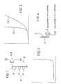
- a protection circuit 10 which comprises a threshold member 12 comprising of three cascade, diode-connected MOS transistors 14, interposed between ground and the base of a bipolar transistor 16 acting as an amplifier member 18.
- the emitter of such a bipolar transistor 16 is connected to the voltage V CC to be stabilized and its collector is connected to ground.
- FIGURE 2 The I/V characteristic curve of such a circuit is shown in FIGURE 2, which represents the noticeable amplification effect that can be achieved when the applied voltage becomes greater than a certain value that, in this case, is given by the sum of the threshold voltage of the threshold member 12 and of the V BE voltage of the amplifier transistor.
- FIGURE 3 a comparison is shown between the outline (a) relating to the threshold member 12 alone and appearing rather poor and unsuitable to offer any protection from over voltages, and the outline (b) relating to the combined assembly of both members and the steepness of which nearly corresponds to the one of a Zener member and is guarantee of a safe protection.
- the amplifier member is implemented by exploiting the bipolar transistors 16 achievable in conventional MOS process.
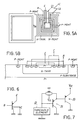
- a composite transistor or double transistor is shown in FIGURE 4; more precisely, the combination is shown of a vertical PNP transistor having its collector coinciding with the substrate and of a lateral PNP transistor with double collector C1-C2.
- FIGUREs 5A-B shows the various design stages of a CMOS process in detail (in this case, a N-TANK process) by which the structure shown in FIGURE 4 can be achieved.
- FIGURE 9 also includes a reference member 20 (that can be made, as in the first embodiment, by three draingate diode-connected, N-channel, MOS transistors 22, as in FIGURE 8) and an amplifier member comprising of a bipolar transistor 24, as in the first embodiment, but having two collectors, and of a N-channel 26, MOS transistor.
- a reference member 20 that can be made, as in the first embodiment, by three draingate diode-connected, N-channel, MOS transistors 22, as in FIGURE 8) and an amplifier member comprising of a bipolar transistor 24, as in the first embodiment, but having two collectors, and of a N-channel 26, MOS transistor.
- the bipolar transistor has its base B connected to the reference voltage, its emitter E connected to the line whose voltage is to be stabilized, a parasitic collector C P connected to ground and a collector C connected to ground through a resistor R and to the gate G of said N-channel MOS transistor 26.
- the N-channel MOS transistor in turn is inserted with its drain and source regions between the line whose voltage is to be stabilized and ground.
- Collector C of said bipolar transistor effectively operates as a current sensor such that, when a current flows therethrough, the voltage of node N increases until the current MOS transistor is set to its conductive condition.
Landscapes
- Metal-Oxide And Bipolar Metal-Oxide Semiconductor Integrated Circuits (AREA)
- Amplifiers (AREA)
- Bipolar Transistors (AREA)
Applications Claiming Priority (2)
| Application Number | Priority Date | Filing Date | Title |
|---|---|---|---|
| IT47985A IT1240103B (it) | 1990-05-18 | 1990-05-18 | Circuito di protezione mos-bip compatibile con la tecnologia cmos std 2 um. |
| IT4798590 | 1990-05-18 |
Publications (3)
| Publication Number | Publication Date |
|---|---|
| EP0457737A2 true EP0457737A2 (de) | 1991-11-21 |
| EP0457737A3 EP0457737A3 (en) | 1992-09-23 |
| EP0457737B1 EP0457737B1 (de) | 1996-11-20 |
Family
ID=11263795
Family Applications (1)
| Application Number | Title | Priority Date | Filing Date |
|---|---|---|---|
| EP91830206A Expired - Lifetime EP0457737B1 (de) | 1990-05-18 | 1991-05-17 | MOS/BIP-Schutzschaltung |
Country Status (3)
| Country | Link |
|---|---|
| EP (1) | EP0457737B1 (de) |
| DE (1) | DE69123170T2 (de) |
| IT (1) | IT1240103B (de) |
Cited By (2)
| Publication number | Priority date | Publication date | Assignee | Title |
|---|---|---|---|---|
| GB2307364A (en) * | 1995-11-20 | 1997-05-21 | Sony Corp | Voltage clamp circuit; non-contact type information card |
| WO2018111190A1 (en) * | 2016-12-12 | 2018-06-21 | Huawei International Pte. Ltd. | System and method for transmitting a wi-fi or a bluetooth signal using a shared transmitter |
Family Cites Families (5)
| Publication number | Priority date | Publication date | Assignee | Title |
|---|---|---|---|---|
| US3407339A (en) * | 1966-05-02 | 1968-10-22 | North American Rockwell | Voltage protection device utilizing a field effect transistor |
| FR2512598A1 (fr) * | 1981-09-09 | 1983-03-11 | Texas Instruments France | Circuit pour proteger un circuit integre contre les surtensions |
| FR2630867B1 (fr) * | 1988-04-29 | 1995-03-24 | Sgs Thomson Microelectronics | Circuit-integre protege contre les decharges electrostatiques |
| DE58906972D1 (de) * | 1988-08-16 | 1994-03-24 | Siemens Ag | Bipolartransistor als Schutzelement für integrierte Schaltungen. |
| EP0401410B1 (de) * | 1989-06-08 | 1993-12-29 | Siemens Aktiengesellschaft | Schaltungsanordnung zum Schutz elektronischer Schaltungen vor Überspannung |
-
1990
- 1990-05-18 IT IT47985A patent/IT1240103B/it active IP Right Grant
-
1991
- 1991-05-17 EP EP91830206A patent/EP0457737B1/de not_active Expired - Lifetime
- 1991-05-17 DE DE69123170T patent/DE69123170T2/de not_active Expired - Fee Related
Cited By (3)
| Publication number | Priority date | Publication date | Assignee | Title |
|---|---|---|---|---|
| GB2307364A (en) * | 1995-11-20 | 1997-05-21 | Sony Corp | Voltage clamp circuit; non-contact type information card |
| GB2307364B (en) * | 1995-11-20 | 2000-08-23 | Sony Corp | Clamp circuit and non-contact type information card |
| WO2018111190A1 (en) * | 2016-12-12 | 2018-06-21 | Huawei International Pte. Ltd. | System and method for transmitting a wi-fi or a bluetooth signal using a shared transmitter |
Also Published As
| Publication number | Publication date |
|---|---|
| EP0457737A3 (en) | 1992-09-23 |
| DE69123170D1 (de) | 1997-01-02 |
| EP0457737B1 (de) | 1996-11-20 |
| DE69123170T2 (de) | 1997-04-03 |
| IT1240103B (it) | 1993-11-27 |
| IT9047985A0 (it) | 1990-05-18 |
| IT9047985A1 (it) | 1991-11-18 |
Similar Documents
| Publication | Publication Date | Title |
|---|---|---|
| US5781389A (en) | Transistor protection circuit | |
| CA1199688A (en) | Current source circuit having reduced error | |
| EP0907916B1 (de) | Verfahren und vorrichtung zur erzeugung eines stromes mit positivem temperaturkoeffizienten | |
| EP1286143A2 (de) | Vergleichs- und Verstärkerschaltung für Detektoren | |
| JPH0679262B2 (ja) | 参照電圧回路 | |
| US7646246B2 (en) | Semiconductor device | |
| US6404275B1 (en) | Modified current mirror circuit for BiCMOS application | |
| US4602207A (en) | Temperature and power supply stable current source | |
| EP1181773B1 (de) | Überspannungsschutz | |
| KR20000075637A (ko) | 전류 리미터 회로 | |
| KR100364876B1 (ko) | 보호회로 | |
| EP0457737A2 (de) | MOS/BIP-Schutzschaltung | |
| US7485931B2 (en) | Semiconductor integrated circuit | |
| JP3483721B2 (ja) | 発光ダイオード駆動回路 | |
| US5132566A (en) | BiMOS semiconductor integrated circuit having short-circuit protection | |
| EP0921619A2 (de) | Stromversorgungsschaltung für eine integrierte Halbleiterschaltung | |
| JP2768855B2 (ja) | 半導体装置 | |
| US20020000864A1 (en) | Semiconductor integrated circuit device using substrate bising and device control method thereof | |
| JP2994293B2 (ja) | バンド・ギャップ・レファレンス回路 | |
| JP2802441B2 (ja) | 複合型半導体定電圧発生回路装置 | |
| JP2666601B2 (ja) | ピークホールド回路 | |
| JP3380308B2 (ja) | 光半導体リレー装置 | |
| JP2970841B2 (ja) | 基準電圧源回路 | |
| JPH0413692Y2 (de) | ||
| JPH058584B2 (de) |
Legal Events
| Date | Code | Title | Description |
|---|---|---|---|
| PUAI | Public reference made under article 153(3) epc to a published international application that has entered the european phase |
Free format text: ORIGINAL CODE: 0009012 |
|
| AK | Designated contracting states |
Kind code of ref document: A2 Designated state(s): DE FR GB IT NL |
|
| PUAL | Search report despatched |
Free format text: ORIGINAL CODE: 0009013 |
|
| AK | Designated contracting states |
Kind code of ref document: A3 Designated state(s): DE FR GB IT NL |
|
| 17P | Request for examination filed |
Effective date: 19930315 |
|
| 17Q | First examination report despatched |
Effective date: 19940622 |
|
| GRAG | Despatch of communication of intention to grant |
Free format text: ORIGINAL CODE: EPIDOS AGRA |
|
| GRAH | Despatch of communication of intention to grant a patent |
Free format text: ORIGINAL CODE: EPIDOS IGRA |
|
| GRAH | Despatch of communication of intention to grant a patent |
Free format text: ORIGINAL CODE: EPIDOS IGRA |
|
| GRAA | (expected) grant |
Free format text: ORIGINAL CODE: 0009210 |
|
| AK | Designated contracting states |
Kind code of ref document: B1 Designated state(s): DE FR GB IT NL |
|
| PG25 | Lapsed in a contracting state [announced via postgrant information from national office to epo] |
Ref country code: NL Free format text: LAPSE BECAUSE OF FAILURE TO SUBMIT A TRANSLATION OF THE DESCRIPTION OR TO PAY THE FEE WITHIN THE PRESCRIBED TIME-LIMIT Effective date: 19961120 |
|
| ITF | It: translation for a ep patent filed | ||
| REF | Corresponds to: |
Ref document number: 69123170 Country of ref document: DE Date of ref document: 19970102 |
|
| ET | Fr: translation filed | ||
| NLV1 | Nl: lapsed or annulled due to failure to fulfill the requirements of art. 29p and 29m of the patents act | ||
| PLBE | No opposition filed within time limit |
Free format text: ORIGINAL CODE: 0009261 |
|
| STAA | Information on the status of an ep patent application or granted ep patent |
Free format text: STATUS: NO OPPOSITION FILED WITHIN TIME LIMIT |
|
| 26N | No opposition filed | ||
| REG | Reference to a national code |
Ref country code: GB Ref legal event code: IF02 |
|
| PGFP | Annual fee paid to national office [announced via postgrant information from national office to epo] |
Ref country code: DE Payment date: 20030530 Year of fee payment: 13 |
|
| PGFP | Annual fee paid to national office [announced via postgrant information from national office to epo] |
Ref country code: GB Payment date: 20040406 Year of fee payment: 14 |
|
| PGFP | Annual fee paid to national office [announced via postgrant information from national office to epo] |
Ref country code: FR Payment date: 20040503 Year of fee payment: 14 |
|
| PG25 | Lapsed in a contracting state [announced via postgrant information from national office to epo] |
Ref country code: DE Free format text: LAPSE BECAUSE OF NON-PAYMENT OF DUE FEES Effective date: 20041201 |
|
| PG25 | Lapsed in a contracting state [announced via postgrant information from national office to epo] |
Ref country code: IT Free format text: LAPSE BECAUSE OF NON-PAYMENT OF DUE FEES;WARNING: LAPSES OF ITALIAN PATENTS WITH EFFECTIVE DATE BEFORE 2007 MAY HAVE OCCURRED AT ANY TIME BEFORE 2007. THE CORRECT EFFECTIVE DATE MAY BE DIFFERENT FROM THE ONE RECORDED. Effective date: 20050517 Ref country code: GB Free format text: LAPSE BECAUSE OF NON-PAYMENT OF DUE FEES Effective date: 20050517 |
|
| GBPC | Gb: european patent ceased through non-payment of renewal fee |
Effective date: 20050517 |
|
| PG25 | Lapsed in a contracting state [announced via postgrant information from national office to epo] |
Ref country code: FR Free format text: LAPSE BECAUSE OF NON-PAYMENT OF DUE FEES Effective date: 20060131 |
|
| REG | Reference to a national code |
Ref country code: FR Ref legal event code: ST Effective date: 20060131 |
|
| PGFP | Annual fee paid to national office [announced via postgrant information from national office to epo] |
Ref country code: IT Payment date: 20070628 Year of fee payment: 17 |
|
| PGRI | Patent reinstated in contracting state [announced from national office to epo] |
Ref country code: IT Effective date: 20091201 |
|
| PGRI | Patent reinstated in contracting state [announced from national office to epo] |
Ref country code: IT Effective date: 20091201 |