EP0456029B1 - Transducteur de pression à élément vibrant - Google Patents
Transducteur de pression à élément vibrant Download PDFInfo
- Publication number
- EP0456029B1 EP0456029B1 EP91106472A EP91106472A EP0456029B1 EP 0456029 B1 EP0456029 B1 EP 0456029B1 EP 91106472 A EP91106472 A EP 91106472A EP 91106472 A EP91106472 A EP 91106472A EP 0456029 B1 EP0456029 B1 EP 0456029B1
- Authority
- EP
- European Patent Office
- Prior art keywords
- layer
- covering
- diaphragm
- vibrator beam
- vibrator
- Prior art date
- Legal status (The legal status is an assumption and is not a legal conclusion. Google has not performed a legal analysis and makes no representation as to the accuracy of the status listed.)
- Expired - Lifetime
Links
Images


Classifications
-
- G—PHYSICS
- G01—MEASURING; TESTING
- G01P—MEASURING LINEAR OR ANGULAR SPEED, ACCELERATION, DECELERATION, OR SHOCK; INDICATING PRESENCE, ABSENCE, OR DIRECTION, OF MOVEMENT
- G01P15/00—Measuring acceleration; Measuring deceleration; Measuring shock, i.e. sudden change of acceleration
- G01P15/02—Measuring acceleration; Measuring deceleration; Measuring shock, i.e. sudden change of acceleration by making use of inertia forces using solid seismic masses
- G01P15/08—Measuring acceleration; Measuring deceleration; Measuring shock, i.e. sudden change of acceleration by making use of inertia forces using solid seismic masses with conversion into electric or magnetic values
- G01P15/097—Measuring acceleration; Measuring deceleration; Measuring shock, i.e. sudden change of acceleration by making use of inertia forces using solid seismic masses with conversion into electric or magnetic values by vibratory elements
-
- G—PHYSICS
- G01—MEASURING; TESTING
- G01L—MEASURING FORCE, STRESS, TORQUE, WORK, MECHANICAL POWER, MECHANICAL EFFICIENCY, OR FLUID PRESSURE
- G01L9/00—Measuring steady of quasi-steady pressure of fluid or fluent solid material by electric or magnetic pressure-sensitive elements; Transmitting or indicating the displacement of mechanical pressure-sensitive elements, used to measure the steady or quasi-steady pressure of a fluid or fluent solid material, by electric or magnetic means
- G01L9/0001—Transmitting or indicating the displacement of elastically deformable gauges by electric, electro-mechanical, magnetic or electro-magnetic means
- G01L9/0008—Transmitting or indicating the displacement of elastically deformable gauges by electric, electro-mechanical, magnetic or electro-magnetic means using vibrations
- G01L9/0019—Transmitting or indicating the displacement of elastically deformable gauges by electric, electro-mechanical, magnetic or electro-magnetic means using vibrations of a semiconductive element
-
- G—PHYSICS
- G01—MEASURING; TESTING
- G01P—MEASURING LINEAR OR ANGULAR SPEED, ACCELERATION, DECELERATION, OR SHOCK; INDICATING PRESENCE, ABSENCE, OR DIRECTION, OF MOVEMENT
- G01P15/00—Measuring acceleration; Measuring deceleration; Measuring shock, i.e. sudden change of acceleration
- G01P15/02—Measuring acceleration; Measuring deceleration; Measuring shock, i.e. sudden change of acceleration by making use of inertia forces using solid seismic masses
- G01P15/08—Measuring acceleration; Measuring deceleration; Measuring shock, i.e. sudden change of acceleration by making use of inertia forces using solid seismic masses with conversion into electric or magnetic values
- G01P15/0802—Details
Definitions
- the present invention relates to a vibrating type pressure measuring device, in which the vibrator beam formed on a silicon substrate is let to vibrate in the natural frequency of the vibrator beam thereof, and detects the change of the vibration frequency generated in the vibrator beam in correspondence to the change of the force applied to the substrate, and together with that, the resonance of the measuring diaphragm due to the vibration of the vibrator beam is prevented, and together with that, the destruction of the measuring diaphragm due to the shock wave-like measuring pressure is also prevented.
- the present invention relates to a vibrating type transducer in which the vibrator beam does not adhere to the wall surface of a vacuum chamber, even if there is such a case that the vibrator beam contacts to the wall surface of the vacuum chamber by the external disturbance such as shock, etc., and buckling, etc., and returns perfectly to the initial state, when the external disturbance is removed.
- Figs. 1 to 4 are constitutional diagrams for showing the constitution of an embodiment of the conventional vibrating type pressure measuring device, for example, shown in USP No. 4841775 as a perspective diagram.
- Fig. 2 is a constitutional diagram in which the A part in Fig. 1 is enlarged, and a vibration detecting circuit has been connected thereto,
- Fig. 3 a sectional diagram for showing A-A′ sectional surface in Fig. 2,
- Fig. 4 an explanatory diagram in which the constitution shown in Fig. 2 has been shown by an electrical equivalent circuit.
- numeral 10 denotes a substrate of the silicon single crystal of the conduction type of D type, in which the upper surface thereof has the crystalline plane of (100), for example, of the impurity concentration of less than 1015 atoms/cm3.
- a diaphragm 11 On one surface of this substrate 10, there is formed a diaphragm 11 by being engraved by etching from the back surface, in thin thickness.
- the thick thickness part 12 in the circumferential part of this diaphragm 11 is adhered to a pedestal 14 having a pressure conducting hole 13 in the center, and further, this pedestal 14 is adhered to a pressure conducting pipe 15 in such a manner as it communicates to the pressure conducting hole 13, and the pressure P to be measured is introduced in this pressure conducting pipe 15.
- this diaphragm 11 On the surface of the side not subjected to the above-described etching of this diaphragm 11 shown with a symbol A, there is formed partially an n+ diffusion layer (abridged in the figure) of the impurity concentration of about 1017, and on one part of this n+ diffusion layer, is formed the vibrator 16 in the direction of the crystal axis ⁇ 001 ⁇ (Fig. 2).
- the n+ layer and the D layer are processed by use of the technologies of the photolithography and the underetching.
- Numeral 17 denotes a magnet provided in non-contact state and perpendicularly to the vibrator 16 at about the central upper part of the vibrator 16, and numeral 18 denotes an SiO2 film as an insulating film (cf. Fig. 3).
- Numerals 19a and 19b denote metal electrodes such as aluminium, etc., and a terminal of this metal electrode 19a is connected to the n+ layer elongated from the vibrator 16 through a contact hole 20a provided via the SiO2 layer, and another terminal thereof is connected to a terminal of a comparative resistance R c , which has approximately equal resistance value to that of the vibrator 16, and the input terminal of an amplifier 21, respectively. From the output terminal of the amplifier 21, together with that output signals are taken out, it is connected to a terminal of the primary coil L1 of a transformer 22. Another terminal of this coil L1 is connected to a common line.
- another terminal of the comparative resistance R c is connected to a terminal of the secondary coil L2 of the transformer 22 in which the midpoint is connected to the common line, and another terminal of this secondary coil L2 is connected to the metal electrode 19b formed on another terminal of the vibrator 16 via contact hole 20b to the n+ layer.
- the impedance R of the vibrator beam 16 rises up in the natural frequency.
- This impedance R can be represented by the following equation. R ⁇ (1/222) ⁇ (1/(Eg ⁇ ) 1/2 ) ⁇ (AB2l2/bh2) ⁇ Q + R d , wherein,
- the vibrator may be used the one formed in the p type, for example, by diffusing B (boron) to the n type silicon substrate for more than 4x10¹⁹ atoms /cm3 and by means of selective etching.
- B boron
- a squeeze RE is provided in the pressure conducting hole 13, and by providing a suitable time constant by the volume CV of the pressure measuring chamber around the silicon diaphragm 11, the destruction of the silicon diaphragm 11 by the shock-like measuring pressure is prevented.
- the silicon diaphragm 11 since the silicon diaphragm 11 has resonance characteristics, it is designed in such a manner as described in the following.
- Fig. 5 the ordinate represents dB and the abscissa the frequency.
- the symbol f0 denotes the resonance frequency of the silicon diaphragm 11, and G0 the amplitude ratio at the resonance point.
- Fig. 6 the ordinate represents dB and the abscissa the frequency.
- the symbol f c represents the shut-down frequency of the pressure conducting line G L the amplitude ratio, CV the volume, and RE the squeeze.
- the pressure conducting line frequency characteristics must be designed in such a manner that it becomes such as G0 + G L ⁇ 0 dB. In this case,
- a pressure measuring apparatus using vibratable wire is suitable for detecting the vibration frequency of the vibrator, and for detecting the frequency output as a digital output. Since it is a digital output, it has high resolution and high S/N ratio, but since the vibrator is made of metal, it has the defect of generating the drift and hysteresis.
- WO-A-88/07185 describes an isolator apparatus suitable to prevent destruction on a diaphragm by a shock-like pressure.
- This apparatus uses external isolation (“seal”) diaphragms in combination with a coupling (“charging”) fluid to transmit pressure via communicating conduits "(holes") to a sensitive sensing diaphragm located in a central cavity within the apparatus' main body.
- the present invention provides a vibrating type pressure measuring device as specified in claim 1.
- Fig. 24 is an essential part constitution explanatory diagram of the use example of the vibrator beam of the present invention
- Fig. 25 is an essential part constitution explanatory diagram of a different embodiment of the present invention
- Figs. 26 to 32 are production procedure explanatory diagrams of Fig. 25
- Fig. 33 is an essential part constitution explanatory diagram of another embodiment of the present invention
- Figs. 34 to 42 are production procedure explanatory diagrams of Fig. 33
- Fig. 43 is an essential part constitution explanatory diagram of the different embodiment of the present invention
- Figs. 44 to 50 are the production procedure explanatory diagrams of Fig. 43
- Fig. 51 is a performance explanatory diagram of Fig. 43
- Fig. 52 is an essential part constitution explanatory diagram of another embodiment of the present invention
- Figs. 53 to 59 are the production procedure explanatory diagrams of Fig. 52
- Fig. 60 is the performance explanatory diagram of Fig. 52.
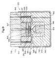
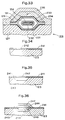
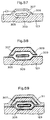
- Fig. 8 is an essential part constitution explanatory diagram of an embodiment of the present invention
- Fig. 9 is an essential part detailed diagram of Fig. 8
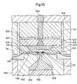
- Fig. 10 is an essential part detailed diagram of Fig. 9.
- numeral 101 denotes a block-like body, 102 an internal chamber provided in the inside of the body 101, and 103 a center diaphragm for dividing the inside chamber 102 into two center chambers 104 and 105.
- the ones denoted by the numerals 111 and 112 are provided in the external side surface of the body 101, and are seal diaphragms for constituting the body 101 and the seal chambers 113 and 114.
- Numerals 115 and 116 denote back up nests provided in the body 101 in opposition to the seal diaphragms 111 and 112.
- Numeral 117 is a communicating hole for communicating the center chambers 104 and 105 and the seal chambers 113 and 114.
- Numeral 118 is a housing having one surface connected to the body 101 and an inside vacant space 119.
- Numeral 120 is a sensor part comprising a supporting body 121, a substrate 122, a chip part 123, and a vibrator beam 124.
- the supporting body 121 is provided in the internal vacant space 119.
- the substrate 122 has one surface supported by the supporting body 121, and consists of silicon.
- the chip part 123 has a diaphragm 127 formed with a concave part 126, and a measuring chamber of one side 128 constituted of the substrate 122 and the concave part 126, and consists of silicon.
- the vibrator beam 124 is provided in the diaphragm 127 by keeping a vacant space 131.
- the part between the vacant space 131 and the external surface of the chip part 123 constitutes a shell 129.
- Numeral 140 denotes a DC applying means, and comprises a spacer 141, a permanent magnet 142, a yoke 143, and a yoke holder 144, and constitutes the sensor part 120 and the measuring chamber 145 of another side, and applies DC magnetic field to the above-described vibrator beam.
- the spacer 141 has one surface fixed in the housing 118, and is provided in the circumference of the supporting body 121, substrate 122, and chip part 123.
- the permanent magnet 142 is arranged in opposition to the vibrator beam 124.
- the yoke 143 preserves the permanent magnet 142 and applies perpendicularly intersecting magnetic flux to the axial direction of the vibrator beam 124, and together with that, has one surface approached to the diaphragm 127, and constitutes a required narrow vacant space 145 with the diaphragm 127.
- the yoke holder 144 holds the yoke 143, and is fixed to the spacer 141.
- Numeral 151 denotes a cap body of U letter shaped cross section having elasticity for setting the relative position of the vibrator beam 124 and the magnet 142 with good precision, and consists of a material having thermal expansion coefficient nearly equal to that of the yoke holder 144 and the housing 118, and it has such a construction that the yoke holder 144 is fitted in a gap in the bottom part 152, which presses the yoke holder 144 to the spacer 141, and in the open hole part 153 side, the housing 118 is fitted in the gap and is welded 155 and fixed to the housing 118 at the open port peripheral part 154.
- Numeral 161 denotes a communicating hole for communicating the measuring chamber 128 of one side to the one side 105 of the center chamber.
- Numeral 162 denotes a communicating hole for communicating the measuring chamber 145 of another side to the another side 106 of the center chamber.
- Numerals 163 and 160 are non-compressive charged liquids respectively charged in two chambers constituted of the seal chambers 113 and 114, communicating holes 117, 161 and 162, center chambers 105 and 106, internal vacant space 119, and measuring chambers 128 and 145.
- silicon oil is used as the charged liquids.
- the differential pressure applied to the seal diaphragms 111 and 112 is transmitted to the measuring chambers 128 and 145, respectively, via communicating holes 161 and 162, and let the diaphragm 127 be displaced in correspondence to the differential pressure.
- the axial power of the vibrator beam 124 fixed at both ends to the diaphragm 127 is changed.
- the vibrator beam 124 is constituted in such a manner that it vibrates at the natural frequency of the vibrator beam 124 by the magnetic field of the DC applying means 140 and the closed loop self exciting vibration circuit (described in the following) connected to the vibrator beam 124.
- the measuring pressure can be measured.
- the diaphragm 127 does not resonance to the vibrator beam 124, by being damped by the yoke 143 arranged to hold a predetermined gap in opposition to the measuring diaphragm 127, the interval dimension of a predetermined gap 146, and the viscocity resistance of the charged liquid 164 intervened in the gap 146.
- the frequency answering characteristics of the measuring diaphragm 127 is constituted in such a manner that it becomes less than the critical attenuation for the external shock wave measuring pressure, the pressure is perfectly damped, and a flat frequency answer can be obtained till the resonance frequency of the measuring diaphragm 127.
- the diaphragm 127 has the resonance frequency determined by the shape thereof, but it is braked by the silicon oil 154 intervened in the gap between the diaphragm 127 and the yoke 143, and the diaphragm 127 can be made not to resonance, even if the vibration frequency number of the vibrator beam 124 agrees to the resonance frequency of the diaphragm 127.
- this condition is sufficiently attained in a silicon oil of 100 cs by the gap 146 of ⁇ 0.1 mm between the yoke 143 and the diaphragm 127.
- Fig. 11 shows an example in which the relationship of Q of the diaphragm 127 and the gap 146 in various kinds of fluids has been actually measured. It has been known that at Q ⁇ 0.7, the influence of the resonance of the diaphragm 127 becomes little.
- the symbol A shows the case where the charged liquid 164 is the atmosphere, B the case of Freon®, and C the case of silicon.
- the device since by the yoke 143 arranged by keeping a predetermined gap 146 in opposition to the diaphragm 127, the interval dimension h of the predetermined gap 146, and the viscocity resistance of the charged liquid 164 intervened in the gap, the device is constituted in such a manner that the frequency answering characteristics of the diaphragm 127 for the external shock wave measuring pressure become less than the critical attenuation, so that it is perfectly damped, and flat frequency answer can be obtained till the resonance frequency of the diaphragm 127.
- Fig. 12 is shown the relationship between the gap dimension h and the frequency wave characteristics of the device.
- the frequency wave characteristic shown by the gap h c shows the frequency wave characteristic curve of the present invention.
- the housing 118 and the yoke holder are fitted in the gap, and the bottom part 152 is made push the yoke holder 144 and the spacer 141 in the direction of the vibrator beam 124, and since the open port peripheral part 154 of the cap body 151 has been fixed to the housing 118 by welding 155, so that since the cap body 151 can push the yoke holder 144 to the housing 118, the relative position of the housing and the yoke-holder can be correctly assured. Therefore, the relative position of the vibrator beam 124 and the magnet 142 in the perpendicular direction to the axis of the cap body 124 can be assembled with good precision and correctly.
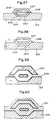
- Fig. 13 is an essential part constitution explanatory diagram of another embodiment of the present invention.
- a rigid body wall 165 has been provided in opposition to the internal side surface of the diaphragm 127.
- Fig. 14 is an essential part constitution explanatory diagram of another embodiment of the present invention.
- the diaphragm 127 and the rigid body wall 166 has been provided in one united constitution.
- Fig. 15 is an essential part constitution explanatory diagram of another embodiment of the present invention.
- the surface of the vibrator 3 is a mirror surface, and since the surface roughness is little and the surface is active, when the vibrator 3 contacts to the wall surface of the diaphragm 11 by external disturbance such as the shock, etc. or the buckling, etc. due to a large compression force, there happens to generate such a case that the vibrator as it is, adheres to the wall surface of the diaphragm.
- the side wall surface of the diaphragm 11 is made be an inclined surface, and the side surface of the legthwise direction of the vibratoror 3 just touches to this inclined surface to form a line contact.
- numeral 167 denotes a rough surface or an uneven surface provided on the wall surface 132 of the diaphragm 127 or on the surface of the vibrator beam 124 in such a manner as that the vibrator beam 124 does not adhere to the wall surface 132 of the diaphragm 127.
- the surface provided on the wall surface 132 of the diaphragm 127 consists of a polysilicon layer having a large surface.
- the vibrator beam 124 even if there is such a case that the vibrator beam 124 contacts to the wall surface of the diaphragm 127 due to the external disturbance such as shock, etc. or buckling, etc., the vibrator beam 124 does not adhere on the wall surface 132 of the diaphragm 127 due to the existence of the rough surface 167, and when the external disturbance has been removed, the device can perfectly return to the initial state.
- the wall surface 132 of the diaphragm 127 is a mirror surface, since the surface roughness is little and the surface is active, although there is such a fear that the vibrator beam 124, as it is, adheres to the wall surface 132 of the diaphragm 127, when the vibrator beam 124 contacts to the wall surface 132 of the diaphragm 127, but since the wall surface 132 of the diaphragm has been made be covered with a polysilicon layer 167, there is no such case that the vibrator beam 124 adheres to the wall surface 132 of the diaphragm 127, and the reliability of the device can be improved.
- the polysilicon layer 167 may be provided on the total surface of the wall surface 132 of the diaphragm 127.
- Such a chip part 123 as described above is prepared, for example, as shown in Figs. 16 to 22.
- Fig. 23 is an essential part constitution explanatory diagram of another embodiment of the present invention, and is an enlarged diagram centered at the part of the vibrator beam 124.
- the constitution having the same symbol as that in Fig. 8 represents the same function.
- Numeral 182 denotes a rough surface provided on the one surface in the side of the shell 129 of the vibrator beam 124.
- the vibrator beam 124 since a rough surface 182 is provided on one surface in the side of the shell 129 of the vibrator beam 124, even in the case when the vibrator beam 124 contacts to the wall surface 132 of the diaphragm 127, the vibrator beam 124 does not adhere to the wall surface 132 of the diaphragm 127 due to the existence of the rough surface 182, and can perfectly return to the initial state, when the external disturbance is removed.
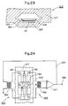
- Fig. 24 is an essential part constitution explanatory diagram of the use example of the vibrator beam of the present invention.
- numeral 124 denotes an vibrator beam in which both terminals are fixed on the diaphragm 127, and are equipped with two first vibrators 191 and the second vibrator 192 for mechanically connecting the node parts of the vibration of the first vibrators 191.
- Numeral 193 denotes the vibration exciting means for exciting the vibrator beam 124 by the magnetic induction action to the direction for perpendicularly intersecting the magnetic field and current by letting AC current flow to the both terminals of the first vibrator 191 of one side by an input transformer 194 by applying perpendicularly intersecting magnetic field to the vibrator beam 124 with a magnet 143.
- the secondary side is connected to the both terminals of the first vibrator 191 of one side.
- Numeral 195 denotes the vibration detecting means for detecting the electromotive force generated in both terminals of another first vibrator 191.
- an output transformer 196 and an amplifier 197 are used.
- the primary side of the output transformer 196 is connected to both terminals of another first vibrator 191, and the secondary side is connected to the output terminal 198 via the amplifier 197, and together with that, is diverged and connected to the primary side of the input transformer 194, and constitutes as a whole a positive feed back self exciting vibration circuit.
- the vibration of the vibrator beam 124 is detected by the vibration detecting means 195, and is taken out as output signals.
- the rough surface may be provided on the whole of the wall surface of the diaphragm 132 or on the whole surface of the vibrator beam 124, and in short, it may be such one in which the vibrator beam 124 does not adhere to the diaphragm wall surface 132. Also, it is needless to say that it is not a rough surface but is an uneven surface.
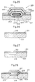
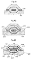
- Fig. 25 is an essential part constitution explanatory diagram of another embodiment of the present invention, and is an enlarged diagram centered to the part of the vibrator beam 124.
- the constitution of the same symbol as that in Fig. 8 represents the same function.
- Numeral 201 denotes the first layer consisting of the oxide film or nitride film provided by covering the surface of the vibrator beam 124.
- Numeral 202 denotes the second layer consisting of polysilicon having rough surface and provided by covering the surface of the first layer 201.
- Numeral 203 denotes the third layer consisting of oxide film or nitride film provided by covering the wall surface 132 of the wall surface 132.
- Numeral 204 denotes the fourth layer consisting of polysilicon provided by covering the surface of the third layer 203.
- Numeral 205 d notes the fifth layer consisting of oxide film or nitride film provided by covering the external surface of the shell 129.
- Numeral 206 denotes the sixth layer consisting of polysilicon provided by covering the surface of the fifth layer 205.
- the vibrating type transducer of the embodiment of Fig. 25 is produced as shown in Figs. 26 to 32.
- the surface of the vibrator beam 124 is a mirror surface, and its surface roughness is little and it is active, although there is such a fear that when the vibrator beam 124 contacts to the wall surface of the shell 129 by the external disturbance such as shock, etc. or buckling, etc. due to a large compression force, it adheres, as it is, on the wall surface of the shell 129, but since the surface of the vibrator beam 124 has been made be covered with the second layer consisting of polysilicon having rough surface, the vibrator beam 124 does not adhere to the wall surface of the shell 129, and reliability of the device is improved.
- Fig. 33 is an essential part constitution explanatory diagram of another embodiment of the present invention and an enlarged diagram centered at the part of the vibrator beam 124.
- the constitution of the same symbol as that in Fig. 8, represents the same function.
- Numeral 231 denotes the first layer consisting of an oxide film or a nitride film provided by covering the surface of the vibrator beam 124.
- Numeral 232 denotes the second layer consisting of polysilicon of a rough surface provided by covering the surface of the first layer 231.
- Numeral 233 denotes the third layer consisting of an oxide film or a nitride film provided by covering the wall surface 132 of the diaphragm 127.
- Numeral 234 denotes the fourth layer consisting of polysilicon provided by covering the surface of the third layer 223.
- Numeral 235 denotes the seventh layer consisting of a silicon single crystal provided by covering the external surface of the shell 129.
- the vibrating type transducer of the embodiment of Fig. 33 is produced in such a manner as described in Figs. 34 to 42.
- the n type fifth epitaxial growth layer 253 is formed on the external surface of the fourth epitaxial layer 247 and the external surface of the chip part 123.
- the surface roughness of the polysilicon layer 252 in this case is about 0.1 ⁇ m in the pitch interval.
- the surface of the vibrator beam 124 is a mirror surface, and the surface roughness is little and the surface is active, when the vibrator beam 124 contacts to the wall surface of the shell 129 due to the external disturbance such as shock, etc. and buckling, etc. by a large compression force, there is the fear that the vibrator beam, as it is, adheres on the wall surface of the shell 129, but since the surface of the vibrator beam 124 has been made be covered by the second layer consisting of polysilicon having rough surface, there occurs no such case that the vibrator beam 124 adheres on the surface of the shell 129, and the reliability of the device is improved.
- the surface of the diaphragm 127 in the outside of the shell 129 which has no relationship to the maladhesion countermeasure of the vibrator beam 124, be a single crystal, the strength, elastic characteristics, and stability similar to those of the conventional measuring diaphragm comprising whole single crystals can be obtained.
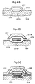
- Fig. 43 is a constitution explanatory diagram of another embodiment of the present invention, and an enlarged diagram centered to the part of the vibrator beam 124.
- the tension of the vibrator beam 124 in the case of being used as a strain gauge gives influence as a gauge factor GF.
- GF (1/2) (0.24 (L/h)2)/(1 + 0.24 (L/h)2 ⁇ o )
- the performance point of the strain gauge is limitted by the working conditions such as, for example, the condition that the boron concentration is more than 3 ⁇ 1019 cm ⁇ 3, and therefore, the crystal strain in the vibrator beam 124 is limitted to about 200 to 300 ⁇ .
- the device has such a defect that the design range capable of being selected becomes narrow due to the restriction of this performance point.
- Numeral 261 denotes the first layer consisting of the oxide film or nitride film provided by covering the surface of the vibrator beam 3.
- Numeral 262 denotes the second layer consisting of polysilicon provided by covering the first layer 261.
- Numeral 263 denotes the third layer consisting of an oxide film or a nitride film provided by covering the wall surface of the diaphragm 132.
- Numeral 264 denotes the fourth layer consisting of polysilicon provided by covering the surface of the third layer 263.
- Numeral 265 denotes the fifth layer consisting of an oxide film or a nitride film provided by covering the external surface of the shell 129.
- Numeral 266 denotes the sixth film consisting of polysilicon provided by covering the surface of the fifth layer 265.
- the tension formed by the vibrator beam 124, the first layer 261, and the second layer 262 is adjusted to a predetermined tension.
- the vibrating type transducer of the embodiment of Fig. 43 is produced in such a manner as shown in Figs. 44 to 50.
- the tension formed by the vibrator beam 124, the first layer 261, and the second layer 262 is adjusted to the predetermined tension.
- the tension T becomes about 100 to 300 ⁇ in dependence to the boron concentratiom.
- the first layer 281 consisting of the oxide film is formed on this vibrator beam 124, a compression force is generated, and since the tension T of the first layer 261 changes with the film thickness of the first layer 261, the tension T of the whole part of the vibrator beam can be regulated.
- the silicon nitride film is formed as the first layer 261, a tensioning force is generated, and since the tension of the first layer 261 changes, the tension T of the whole part of the vibrator beam can be regulated further.
- the tension T of the whole part of the vibrator beam can be made approach to 0, and the tension T as that of the whole part of the vibrator beam can be more easily regulated.
- Fig. 51 the relationship between the silicon oxide film thickness A, the silicon nitride film thickness B, and the temperature coefficient ⁇ is shown.
- the thickness of the silicon oxide film A is shown with a white circle, and the thickness of the silicon nitride film B with a black circle.
- the silicon nitride film is made be as 2000 ⁇ , the total thickness becomes about 700 ⁇ .
- the surface of the vibrator beam 124 is covered with the second layer 262 consisting of polysilicon having rough surface, there occurs no case where the vibrator beam 124 adheres on the wall surface of the shell 129, and the reliability of the device is improved.
- Fig. 52 is an essential part constitution explanatory diagram of another embodiment of the present invention.
- the temperature coefficient of the natural frequency of the silicon vibrator beam 124 is -30 to 40 ppm/K, and this is the value from the physical property values.
- the temperature coefficient is too large for the case of using it in the sensor of high precision, and the stability of the temperature sensor for use of the temperature correction is required.
- the device becomes expensive in the cost, and the stability of the whole device is influenced by the stability of the temperature sensor.
- the embodiment of Fig. 52 intends to solve this problem.
- Numeral 291 denotes the first layer consisting of the oxide film or nitride film provided by covering the surface of the vibrator beam 124.
- Numeral 292 denotes the second layer consisting of polysilicon provided by covering the surface of the first layer 291.
- Numeral 293 denotes the third layer consisting of oxide layer or nitride layer provided by covering the wall surface 132 of the diaphragm 127.
- Numeral 294 denotes the fourth layer consisting of polysilicon provided by covering the surface of the third layer 293.
- Numeral 295 denotes the fifth layer consisting of oxide film or nitride film provided by covering the external surface of the shell 129.
- Numeral 296 denotes the sixth layer consisting of polysilicon provided by covering the surface of the fifth layer 295.
- the temperature coefficient formed by the vibrator beam 124, the first layer 291, and the second layer 292 is adjusted to the predetermined temperature coefficient.
- the vibrating type transducer of the embodiment of Fig. 52 is produced in such a manner as described in Figs. 53 to 59.
- the temperature coefficient formed by the vibrator beam 124, the first layer 291, and the second layer 292 is adjusted to the predetermined temperature coefficient.
- the temperature coefficient ⁇ becomes to be determined by the boron concentration.
- the temperature coefficient of the first layer 291 changes by the film thickness of the first layer 291, the temperature coefficient of the whole vibrator beam part can be regulated to 0.
- the temperature coefficient of the whole vibrator beam part can be regulated to 0.
- the second layer 292 consisting of polysilicon has been provided on the external surface of the first layer 291, it is more easily regulated that the temperature coefficient of the whole vibrator beam part is made 0.
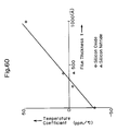
- Fig. 60 is shown the relationship between the silicon oxide film thickness A, the silicon nitride film thickness B, and the temperature coefficient ⁇ in the case when the thickness of the vibrator beam 124 is 3.5 ⁇ m, and the thickness of the second layer is 1 ⁇ m.
- the thickness A of the silicon oxide film is shown with a white circle, and the thickness B of the nitride film with a black circle.
- the constitution of the fifth layer 295 consisting of oxide film or nitride film provided by covering the external surface of the shell 129 and the sixth layer 296 consisting of polysilicon provided by covering the surface of the fifth layer 295 but the constitution is not limitted to this one, and for example, it will do that the epitaxial growth layer consisting of a silicon single layer may be provided by removing the fifth layer 295 consisting of oxide film or nitride film on the external surface of the shell 129, and in effect, it will do that the one constituted in such a manner that it can seal the vibrator beam 124 may be used.
Claims (6)
- Un dispositif de mesure de pression du type vibrant pour mesurer une pression en utilisant le fait que la fréquence naturelle d'un barreau vibrant (124) varie en correspondance avec la variation de la force axiale du barreau vibrant (124), comportant :- une enveloppe (118) présentant un espace intérieur (119),- une partie de détecteur (120) prévue dans ledit espace intérieur (119) et comprenant :-- un corps de support (121) fixé à une surface dudit espace intérieur (119),-- un substrat (122) constitué en silicone et supporté par ledit corps de support (121), et-- une partie de plaquette (123) constituée en silicone et présentant un évidement (126) à sa surface supérieure de manière à définir une membrane de détection (127), ladite partie de plaquette (123) étant fixée à une surface dudit substrat (122) de manière à former une première chambre de mesure entre ledit substrat (122) et ladite membrane de détection (127), ledit barreau vibrant (124) constitué en silicone présentant une cavité sous vide dans ladite membrane de détection (127), ledit barreau vibrant présentant une forme en H dont les quatre parties d'extrémité sont fixées à ladite membrane de détection (127),- des moyens (140) d'application d'un champ magnétique continu prévus dans ledit espace intérieur (119), à distance de ladite membrane de détection, de manière à former une seconde chambre de mesure (145) pour appliquer un champ magnétique continu audit barreau vibrant (124), lesdits moyens (140) d'application d'un champ magnétique continu comportant :caractérisé en ce que ledit dispositif comporte au surplus :-- un aimant permanent (142) disposé en regard dudit barreau vibrant (124) et maintenu à l'intérieur d'une culasse (143), ladite culasse (143) étant à son tour maintenue à l'intérieur d'un porte-culasse (144),-- une entretoise (141) en forme de bague prévue autour dudit corps de support (121), dudit substrat (122) et ladite partie de plaquette (123), et espacée dudit aimant et ladite membrane de détection d'un-intervalle prédéterminé (146),- un corps (101) en forme de bloc présentant une chambre intérieure (102) à l'intérieur de laquelle est placée une membrane centrale (103),- des membranes d'étanchéité (111, 112) prévues sur les surfaces latérales extérieures du corps (101) en forme de bloc et définissant avec celui-ci des première et seconde chambres d'étanchéité (113, 114), ladite membrane centrale (103) divisant ladite chambre intérieure (102) en deux première et seconde chambres centrales (104, 105) dont chacune communique avec l'une respective desdites première et seconde chambres d'étanchéité (113, 114) par l'intermédiaire de premiers orifices de communication (117),- un deuxième orifice de communication (161) pour faire communiquer ladite première chambre de mesure (128) avec l'une (104) desdites première et seconde chambres centrales (104, 105),- un troisième orifice de communication (162) pour faire communiquer ladite seconde chambre de mesure (145) avec l'autre (105) desdites première et seconde chambres centrales (104, 105),- un premier liquide de charge (163) destiné à être chargé dans ladite première chambre d'étanchéité (113), l'un desdits premiers orifices de communication (117), dudit deuxième orifice de communication (161), ladite première chambre centrale (104), dudit espace intérieur (119) et de ladite première chambre de mesure (128), ledit liquide présentant une viscosité prédéterminée de manière à provoquer un amortissement en combinaison avec ledit intervalle prédéterminé (146) entre ladite membrane de détection (127) et ladite culasse (143) et à transmettre, en fonctionnement, une pression PL appliquée à l'une (111) desdites membranes d'étanchéité (111, 112) à une surface de ladite membrane de détection (127),- un second liquide de charge (164) destiné à être chargé dans ladite seconde chambre d'étanchéité (114), l'autre desdits orifices de communication (117), dudit troisième orifice de communication (162), de ladite sesonde chambre centrale (105) et de ladite seconde chambre de mesure (145), et présentant une viscosité prédéterminée pour provoquer un amortissement en combinaison avec ledit intervalle prédéterminé (146) entre ladite membrane de détection (127) et ladite culasse (143) et à transmettre une pression de mesure (PH) appliquée à l'autre (112) desdites membranes d'étanchéité (111, 112) à l'autre surface de ladite membrane de détection (127).
- Un dispositif de mesure de pression du type vibrant tel que revendiqué dans la revendication 1, caractérisé en ce qu'il comporte une surface rugueuse ou surface irrégulière (167) prévue sur la surface de paroi de ladite membrane de détection (127) ou sur la surface dudit barreau vibrant (124).
- Un dispositif de mesure de pression du type vibrant tel que revendiqué dans la revendication 1, caractérisé en ce qu'il comporte une première couche (201) constituée d'une pellicule d'oxyde ou d'une pellicule de nitrure prévue en recouvrant la surface dudit barreau vibrant (124),
une deuxième couche (202) constituée de polysilicone présentant une surface rugueuse prévue en recouvrant la surface de ladite première couche (201),
une troisième couche (203) constituée d'une pellicule d'oxyde ou d'une pellicule de nitrure prévue en recouvrant la surface intérieure (132) dudit intervalle (131), et
une quatrième couche (204) constituée de polysilicone prévue en recouvrant la surface de ladite troisième couche (203),
une cinquième couche (205) constituée d'une pellicule d'oxyde de silicone ou d'une pellicule de nitrure de silicone prévue en recouvrant la surface extérieure d'une coquille (129), et
une sixième couche (206) constituée de polysicone prévue en recouvrant la surface de ladite cinquième couche (205, Fig. 25). - Un dispositif de mesure de pression du type vibrant tel que revendiqué dans la revendication 1, caractérisé en ce qu'il est équipé de :
une première couche (231) constituée d'une pelicule d'oxyde ou d'une pellicule de nitrure prévue en recouvrant la surface dudit barreau vibrant (124),
une deuxième couche (232) constituée d'un polysilicone présentant une surface rugueuse prévue en recouvrant la surface de ladite première couche (231),
une troisième couche (233) constituée d'une pellicule d'oxyde ou d'une pellicule de nitrure prévue en recouvrant la surface intérieure (132) dudit intervalle (131),
une quatrième couche (234) constituée d'un polysilicone prévue en recouvrant la surface de ladite troisième couche (233), et
une septième couche (235) constituée d'un cristal unique de silicone prévue en recouvrant la surface externe d'une coquille (129, Fig. 33) - Un dispositif de mesure de pression du type vibrant tel que revendiqué dans la revendication 1, caractérisé en ce qu'il équipé de
une première couche (261) constituée d'une pellicule d'oxyde ou d'une pellicule de nitrure prévue en recouvrant la surface dudit barreau vibrant (124),
une deuxième couche (262) constituée d'un polysilicone prévue en recouvrant la surface de ladite première couche (261),
une troisième couche (263) constituée d'une pellicule d'oxyde ou d'une pellicule de nitrure prévue sur la surface intérieure (132) dudit intervalle (131) et
une quatrième couche (264) constituée d'un polysilicone prévue en recouvrant la surface de ladite troisième couche (263), dans lequel :
en ajustant l'épaisseur de pellicule de ladite première couche (261) et de ladite deuxième couche (262), la tension formée par le barreau vibrant (124), la première couche (261) et la deuxième couche (262) ci-dessus décrits est ajustée à une tension prédéterminée. - Un dispositif de mesure de pression du type vibrant tel que revendiqué dans la revendication 1, caractérisé en ce qu'il est équipé de
une première couche (291) constituée d'une pellicule d'oxyde ou d'une pellicule de nitrure prévue en recouvrant la surface dudit barreau vibrant (124),
une deuxième couche (292) constituée de polysilicone prévue en recouvrant la surface de ladite première couche (291),
une troisième couche (293) constituée d'une pellicule d'oxyde ou d'une pellicule de nitrure prévue en recouvrant la surface intérieure (132) dudit intervalle (131) et
une quatrième couche (294) constituée de polysilicone prévue en recouvrant ladite troisième couche (293), dans lequel :
en ajustant l'épaisseur de pellicule de ladite première couche (291) et de ladite deuxième couche (292), le coefficient de température formé par le barreau vibrant (124), la première couche (291) et la deuxième couche (292) ci-dessus décrits est ajusté à un coefficient prédéterminé de température.
Applications Claiming Priority (10)
| Application Number | Priority Date | Filing Date | Title |
|---|---|---|---|
| JP12098790A JP2822594B2 (ja) | 1990-05-10 | 1990-05-10 | 振動形トランスデュサ |
| JP120987/90 | 1990-05-10 | ||
| JP121489/90 | 1990-05-11 | ||
| JP12148990A JP2687676B2 (ja) | 1990-05-11 | 1990-05-11 | 振動形トランスデュサ |
| JP123791/90 | 1990-05-14 | ||
| JP12379190A JP2822596B2 (ja) | 1990-05-14 | 1990-05-14 | 振動形トランスデュサ |
| JP182064/90 | 1990-07-10 | ||
| JP18206490A JPH0469536A (ja) | 1990-07-10 | 1990-07-10 | 差圧測定装置 |
| JP19823/91U | 1991-03-29 | ||
| JP1982391U JP2533979Y2 (ja) | 1991-03-29 | 1991-03-29 | 振動形圧力測定装置 |
Publications (2)
| Publication Number | Publication Date |
|---|---|
| EP0456029A1 EP0456029A1 (fr) | 1991-11-13 |
| EP0456029B1 true EP0456029B1 (fr) | 1994-12-14 |
Family
ID=27520172
Family Applications (1)
| Application Number | Title | Priority Date | Filing Date |
|---|---|---|---|
| EP91106472A Expired - Lifetime EP0456029B1 (fr) | 1990-05-10 | 1991-04-23 | Transducteur de pression à élément vibrant |
Country Status (3)
| Country | Link |
|---|---|
| US (1) | US5123282A (fr) |
| EP (1) | EP0456029B1 (fr) |
| DE (2) | DE69105809T2 (fr) |
Families Citing this family (28)
| Publication number | Priority date | Publication date | Assignee | Title |
|---|---|---|---|---|
| US5477737A (en) * | 1991-10-08 | 1995-12-26 | Lew; Hyok S. | Oscillatory pressure transducer |
| US5241864A (en) * | 1992-06-17 | 1993-09-07 | Motorola, Inc. | Double pinned sensor utilizing a tensile film |
| DE4317274A1 (de) * | 1993-05-25 | 1994-12-01 | Bosch Gmbh Robert | Verfahren zur Herstellung oberflächen-mikromechanischer Strukturen |
| US5559358A (en) * | 1993-05-25 | 1996-09-24 | Honeywell Inc. | Opto-electro-mechanical device or filter, process for making, and sensors made therefrom |
| CN1052538C (zh) * | 1993-09-10 | 2000-05-17 | 横河电机株式会社 | 半导体式差压测量装置 |
| DE4332843C2 (de) * | 1993-09-27 | 1997-04-24 | Siemens Ag | Verfahren zur Herstellung einer mikromechanischen Vorrichtung und mikromechanische Vorrichtung |
| JPH07174651A (ja) * | 1993-12-17 | 1995-07-14 | Mitsubishi Electric Corp | 圧力センサ |
| US5501103B1 (en) * | 1994-02-15 | 1998-08-04 | Allied Signal Inc | Two-port electromagnetic drive for a double-ended tuning fork |
| JP3489273B2 (ja) * | 1995-06-27 | 2004-01-19 | 株式会社デンソー | 半導体力学量センサの製造方法 |
| DE753728T1 (de) * | 1995-07-14 | 1997-06-26 | Yokogawa Electric Corp | Halbleiter-Druckdifferenzmessvorrichtung |
| IT1287123B1 (it) * | 1996-10-31 | 1998-08-04 | Abb Kent Taylor Spa | Dispositivo per la misura di una pressione |
| IT1295031B1 (it) | 1997-09-18 | 1999-04-27 | Abb Kent Taylor Spa | Procedimento per la fabbricazione di un dispositivo di misura di pressione dotato di elemento risonante |
| US6198207B1 (en) * | 1998-09-01 | 2001-03-06 | Oceana Sensor Technologies | High-volume production, low cost piezoelectric transducer using low-shrink solder of bismuth or antimony alloy |
| DE10034390C2 (de) * | 2000-07-14 | 2003-06-26 | Eads Deutschland Gmbh | Drucksensor und Verfahren zu seiner Herstellung, sowie Verbrennungskraftmaschine mit Drucksensor |
| JP4269710B2 (ja) | 2002-10-22 | 2009-05-27 | 横河電機株式会社 | 周波数測定回路およびそれを用いた振動センサ式差圧・圧力伝送器 |
| FR2857002B1 (fr) * | 2003-07-04 | 2005-10-21 | Commissariat Energie Atomique | Procede de desolidarisation d'une couche utile et composant obtenu par ce procede |
| US7591187B2 (en) * | 2005-05-10 | 2009-09-22 | Microstrain, Inc. | Wireless vibrating strain gauge for smart civil structures |
| JP5158160B2 (ja) * | 2010-09-10 | 2013-03-06 | 横河電機株式会社 | 振動式トランスデューサ |
| JP2013044675A (ja) * | 2011-08-25 | 2013-03-04 | Yokogawa Electric Corp | 振動式差圧センサとその製造方法 |
| JP5835285B2 (ja) * | 2013-07-24 | 2015-12-24 | 横河電機株式会社 | 振動式トランスデューサおよびその製造方法 |
| JP5807664B2 (ja) | 2013-08-07 | 2015-11-10 | 横河電機株式会社 | 振動式トランスデューサおよびその製造方法 |
| RU2548404C1 (ru) * | 2013-10-25 | 2015-04-20 | Федеральное государственное автономное образовательное учреждение высшего профессионального образования "Санкт-Петербургский государственный университет аэрокосмического приборостроения" | Способ измерения разности давлений датчиком с частотно-модулированным выходным сигналов и датчик для осуществления способа |
| RU2548582C1 (ru) * | 2013-10-25 | 2015-04-20 | Федеральное государственное автономное образовательное учреждение высшего профессионального образования "Санкт-Петербургский государственный университет аэрокосмического приборостроения" | Способ измерения разности давлений датчиком с частотно-модулированным выходным сигналом и датчик для осуществления способа |
| CN105181214A (zh) * | 2015-05-26 | 2015-12-23 | 苏州华徕光电仪器有限公司 | 一种振弦式压力传感器 |
| RU2679640C1 (ru) * | 2018-06-05 | 2019-02-12 | Общество с ограниченной ответственностью "Специальное конструкторское техническое бюро электроники, приборостроения и автоматизации" ООО "СКТБ ЭлПА" | Частоторезонансный чувствительный элемент для датчика дифференциального давления |
| RU2708938C1 (ru) * | 2019-04-19 | 2019-12-12 | Федеральное государственное бюджетное учреждение науки Институт проблем управления им. В.А. Трапезникова Российской академии наук | Устройство для измерения высоких давлений газообразных сред |
| RU2726908C1 (ru) * | 2019-12-13 | 2020-07-16 | Общество с ограниченной ответственностью "Специальное конструкторское техническое бюро электроники, приборостроения и автоматизации" ООО "СКТБ ЭлПА" | Микроэлектронный скважинный датчик абсолютного давления |
| CN114275730B (zh) * | 2021-11-17 | 2023-09-26 | 电子科技大学 | 一种磁振子耦合共振型微纳称重器件与其制备方法 |
Citations (1)
| Publication number | Priority date | Publication date | Assignee | Title |
|---|---|---|---|---|
| WO1988007185A1 (fr) * | 1987-03-12 | 1988-09-22 | Rosemount Inc. | Dispositif d'isolation |
Family Cites Families (4)
| Publication number | Priority date | Publication date | Assignee | Title |
|---|---|---|---|---|
| JPS6263828A (ja) * | 1985-09-06 | 1987-03-20 | Yokogawa Electric Corp | 振動式トランスジューサ |
| GB8610253D0 (en) * | 1986-04-26 | 1986-05-29 | Stc Plc | Resonator device |
| US5009108A (en) * | 1988-09-16 | 1991-04-23 | Yokogawa Electric Corporation | Vibrating type transducer |
| US5060526A (en) * | 1989-05-30 | 1991-10-29 | Schlumberger Industries, Inc. | Laminated semiconductor sensor with vibrating element |
-
1991
- 1991-04-23 DE DE69105809T patent/DE69105809T2/de not_active Expired - Fee Related
- 1991-04-23 DE DE199191106472T patent/DE456029T1/de active Pending
- 1991-04-23 EP EP91106472A patent/EP0456029B1/fr not_active Expired - Lifetime
- 1991-05-02 US US07/694,709 patent/US5123282A/en not_active Expired - Lifetime
Patent Citations (1)
| Publication number | Priority date | Publication date | Assignee | Title |
|---|---|---|---|---|
| WO1988007185A1 (fr) * | 1987-03-12 | 1988-09-22 | Rosemount Inc. | Dispositif d'isolation |
Also Published As
| Publication number | Publication date |
|---|---|
| DE456029T1 (de) | 1992-06-11 |
| DE69105809T2 (de) | 1995-05-11 |
| US5123282A (en) | 1992-06-23 |
| EP0456029A1 (fr) | 1991-11-13 |
| DE69105809D1 (de) | 1995-01-26 |
Similar Documents
| Publication | Publication Date | Title |
|---|---|---|
| EP0456029B1 (fr) | Transducteur de pression à élément vibrant | |
| JP3223358B2 (ja) | 定電界で駆動されるマイクロビームによる共振ゲージ | |
| US5188983A (en) | Polysilicon resonating beam transducers and method of producing the same | |
| US4966649A (en) | Process for manufacturing a vibrating type transducer | |
| EP0451992A2 (fr) | Détection des vibrations d'une poutre micro à travers une enveloppe | |
| JPH0518050B2 (fr) | ||
| US5009108A (en) | Vibrating type transducer | |
| JP4864438B2 (ja) | 圧力を検知するためのシステム及び方法 | |
| JP2004132913A (ja) | 感圧素子、及びこれを用いた圧力センサ | |
| JPH0749281A (ja) | 半導体差圧測定装置の製造方法 | |
| JPH0628662Y2 (ja) | 振動形差圧センサ | |
| JP2687676B2 (ja) | 振動形トランスデュサ | |
| WO2020228738A1 (fr) | Élément sensible à la pression, procédé de préparation d'un élément sensible à la pression et capteur de pression | |
| JP2770488B2 (ja) | 半導体圧力計 | |
| JP2822594B2 (ja) | 振動形トランスデュサ | |
| JPH07103838A (ja) | 微圧センサ | |
| JPH085435A (ja) | ガスメータ | |
| JP3067382B2 (ja) | 差圧測定装置 | |
| Angell | Micromachined silicon transducers for measuring force, pressure, and motion | |
| JPH0431728A (ja) | 半導体圧力計 | |
| Lee | A silicon capacitive pressure transducer: Performance characteristics and limitations | |
| JP2004294359A (ja) | 圧力センサ | |
| JP2822598B2 (ja) | 振動形トランスデュサ | |
| JPS6285470A (ja) | 圧力センサ | |
| JP2000146731A (ja) | 振動型圧力測定装置 |
Legal Events
| Date | Code | Title | Description |
|---|---|---|---|
| PUAI | Public reference made under article 153(3) epc to a published international application that has entered the european phase |
Free format text: ORIGINAL CODE: 0009012 |
|
| 17P | Request for examination filed |
Effective date: 19910517 |
|
| AK | Designated contracting states |
Kind code of ref document: A1 Designated state(s): DE GB NL |
|
| DET | De: translation of patent claims | ||
| 17Q | First examination report despatched |
Effective date: 19930707 |
|
| GRAA | (expected) grant |
Free format text: ORIGINAL CODE: 0009210 |
|
| AK | Designated contracting states |
Kind code of ref document: B1 Designated state(s): DE GB NL |
|
| REF | Corresponds to: |
Ref document number: 69105809 Country of ref document: DE Date of ref document: 19950126 |
|
| PLBE | No opposition filed within time limit |
Free format text: ORIGINAL CODE: 0009261 |
|
| STAA | Information on the status of an ep patent application or granted ep patent |
Free format text: STATUS: NO OPPOSITION FILED WITHIN TIME LIMIT |
|
| 26N | No opposition filed | ||
| REG | Reference to a national code |
Ref country code: GB Ref legal event code: 746 Effective date: 19970326 |
|
| REG | Reference to a national code |
Ref country code: GB Ref legal event code: IF02 |
|
| PGFP | Annual fee paid to national office [announced via postgrant information from national office to epo] |
Ref country code: DE Payment date: 20070419 Year of fee payment: 17 |
|
| PGFP | Annual fee paid to national office [announced via postgrant information from national office to epo] |
Ref country code: GB Payment date: 20070418 Year of fee payment: 17 |
|
| PGFP | Annual fee paid to national office [announced via postgrant information from national office to epo] |
Ref country code: NL Payment date: 20080415 Year of fee payment: 18 |
|
| GBPC | Gb: european patent ceased through non-payment of renewal fee |
Effective date: 20080423 |
|
| PG25 | Lapsed in a contracting state [announced via postgrant information from national office to epo] |
Ref country code: DE Free format text: LAPSE BECAUSE OF NON-PAYMENT OF DUE FEES Effective date: 20081101 |
|
| PG25 | Lapsed in a contracting state [announced via postgrant information from national office to epo] |
Ref country code: GB Free format text: LAPSE BECAUSE OF NON-PAYMENT OF DUE FEES Effective date: 20080423 |
|
| NLV4 | Nl: lapsed or anulled due to non-payment of the annual fee |
Effective date: 20091101 |
|
| PG25 | Lapsed in a contracting state [announced via postgrant information from national office to epo] |
Ref country code: NL Free format text: LAPSE BECAUSE OF NON-PAYMENT OF DUE FEES Effective date: 20091101 |