EP0453716A2 - Anschlussanordnung zum Testen eines Chips - Google Patents
Anschlussanordnung zum Testen eines Chips Download PDFInfo
- Publication number
- EP0453716A2 EP0453716A2 EP91101647A EP91101647A EP0453716A2 EP 0453716 A2 EP0453716 A2 EP 0453716A2 EP 91101647 A EP91101647 A EP 91101647A EP 91101647 A EP91101647 A EP 91101647A EP 0453716 A2 EP0453716 A2 EP 0453716A2
- Authority
- EP
- European Patent Office
- Prior art keywords
- connector
- electronic device
- contact areas
- conductors
- convex
- Prior art date
- Legal status (The legal status is an assumption and is not a legal conclusion. Google has not performed a legal analysis and makes no representation as to the accuracy of the status listed.)
- Granted
Links
Images

Classifications
-
- G—PHYSICS
- G01—MEASURING; TESTING
- G01R—MEASURING ELECTRIC VARIABLES; MEASURING MAGNETIC VARIABLES
- G01R1/00—Details of instruments or arrangements of the types included in groups G01R5/00 - G01R13/00 and G01R31/00
- G01R1/02—General constructional details
- G01R1/04—Housings; Supporting members; Arrangements of terminals
- G01R1/0408—Test fixtures or contact fields; Connectors or connecting adaptors; Test clips; Test sockets
- G01R1/0433—Sockets for IC's or transistors
- G01R1/0483—Sockets for un-leaded IC's having matrix type contact fields, e.g. BGA or PGA devices; Sockets for unpackaged, naked chips
-
- G—PHYSICS
- G01—MEASURING; TESTING
- G01R—MEASURING ELECTRIC VARIABLES; MEASURING MAGNETIC VARIABLES
- G01R1/00—Details of instruments or arrangements of the types included in groups G01R5/00 - G01R13/00 and G01R31/00
- G01R1/02—General constructional details
- G01R1/06—Measuring leads; Measuring probes
- G01R1/067—Measuring probes
- G01R1/073—Multiple probes
- G01R1/07307—Multiple probes with individual probe elements, e.g. needles, cantilever beams or bump contacts, fixed in relation to each other, e.g. bed of nails fixture or probe card
- G01R1/07314—Multiple probes with individual probe elements, e.g. needles, cantilever beams or bump contacts, fixed in relation to each other, e.g. bed of nails fixture or probe card the body of the probe being perpendicular to test object, e.g. bed of nails or probe with bump contacts on a rigid support
-
- H—ELECTRICITY
- H01—ELECTRIC ELEMENTS
- H01R—ELECTRICALLY-CONDUCTIVE CONNECTIONS; STRUCTURAL ASSOCIATIONS OF A PLURALITY OF MUTUALLY-INSULATED ELECTRICAL CONNECTING ELEMENTS; COUPLING DEVICES; CURRENT COLLECTORS
- H01R12/00—Structural associations of a plurality of mutually-insulated electrical connecting elements, specially adapted for printed circuits, e.g. printed circuit boards [PCB], flat or ribbon cables, or like generally planar structures, e.g. terminal strips, terminal blocks; Coupling devices specially adapted for printed circuits, flat or ribbon cables, or like generally planar structures; Terminals specially adapted for contact with, or insertion into, printed circuits, flat or ribbon cables, or like generally planar structures
- H01R12/70—Coupling devices
- H01R12/71—Coupling devices for rigid printing circuits or like structures
- H01R12/712—Coupling devices for rigid printing circuits or like structures co-operating with the surface of the printed circuit or with a coupling device exclusively provided on the surface of the printed circuit
- H01R12/714—Coupling devices for rigid printing circuits or like structures co-operating with the surface of the printed circuit or with a coupling device exclusively provided on the surface of the printed circuit with contacts abutting directly the printed circuit; Button contacts therefore provided on the printed circuit
-
- H—ELECTRICITY
- H01—ELECTRIC ELEMENTS
- H01R—ELECTRICALLY-CONDUCTIVE CONNECTIONS; STRUCTURAL ASSOCIATIONS OF A PLURALITY OF MUTUALLY-INSULATED ELECTRICAL CONNECTING ELEMENTS; COUPLING DEVICES; CURRENT COLLECTORS
- H01R13/00—Details of coupling devices of the kinds covered by groups H01R12/70 or H01R24/00 - H01R33/00
- H01R13/02—Contact members
- H01R13/22—Contacts for co-operating by abutting
- H01R13/24—Contacts for co-operating by abutting resilient; resiliently-mounted
- H01R13/2464—Contacts for co-operating by abutting resilient; resiliently-mounted characterized by the contact point
- H01R13/2485—Contacts for co-operating by abutting resilient; resiliently-mounted characterized by the contact point for contacting a ball
-
- H—ELECTRICITY
- H01—ELECTRIC ELEMENTS
- H01L—SEMICONDUCTOR DEVICES NOT COVERED BY CLASS H10
- H01L2224/00—Indexing scheme for arrangements for connecting or disconnecting semiconductor or solid-state bodies and methods related thereto as covered by H01L24/00
- H01L2224/01—Means for bonding being attached to, or being formed on, the surface to be connected, e.g. chip-to-package, die-attach, "first-level" interconnects; Manufacturing methods related thereto
- H01L2224/10—Bump connectors; Manufacturing methods related thereto
- H01L2224/12—Structure, shape, material or disposition of the bump connectors prior to the connecting process
- H01L2224/13—Structure, shape, material or disposition of the bump connectors prior to the connecting process of an individual bump connector
- H01L2224/13001—Core members of the bump connector
- H01L2224/1302—Disposition
- H01L2224/13021—Disposition the bump connector being disposed in a recess of the surface
-
- H—ELECTRICITY
- H01—ELECTRIC ELEMENTS
- H01R—ELECTRICALLY-CONDUCTIVE CONNECTIONS; STRUCTURAL ASSOCIATIONS OF A PLURALITY OF MUTUALLY-INSULATED ELECTRICAL CONNECTING ELEMENTS; COUPLING DEVICES; CURRENT COLLECTORS
- H01R2201/00—Connectors or connections adapted for particular applications
- H01R2201/20—Connectors or connections adapted for particular applications for testing or measuring purposes
Definitions
- This invention relates to electrical connectors and, more particularly, to an electrical connector adapted to temporarily contacting conductive pads on a semiconductor chip during burn-in or other test procedures.
- solder interconnect areas do not extend a uniform height from the surface of the chip.
- prior art interconnect systems have used connectors which exhibit some flexibility so that the height differences of the solder interconnect areas can be accommodated.
- One such connector employs spring loaded pins which automatically adjust to the various solder heights when pressure is applied between the connector and the chip. Spring-loaded connectors are both expensive and present problems when operated in a high temperature ambient.
- Another type of connector is known as a "probe-card" and includes a plurality of cantilevered, flexible beams which independently make contact with the various solder interconnect areas as the probe-card is brought down upon the chip. Because of the size of the probe-card, the number of chips which can be contacted is limited and registration between multiple chips and the probe card is difficult to achieve.
- Patent 3,862,790 to Davies et al. another interconnection scheme is shown wherein a plurality of parallel conductors are held in a block of insulating material.
- circuit boards to be interconnected via the parallel conductors, they are placed on either side of the interconnection matrix and pressed together-and, the insulating material yields slightly to enable the conductors to make the desired connections.
- the present invention as claimed discloses an electrical connector for making contact with a plurality of convex and deformable contacts on an electronic device.
- the electrical connector comprises a substrate having a plurality of conductors which extend above its surface.
- a polymeric material is disposed on the surface of the substrate and has openings which expose the conductors, each opening sized to receive one of the convex, deformable contacts, and to enable electrical connection between the exposed conductors and the deformable contacts.
- a mechanism is provided for urging the deformable contacts on the electronic device against the exposed conductors. The mechanism exerts sufficient force between the device and the conductors to cause some deformation of the convex contact areas by the conductors.
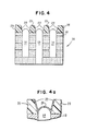
- a plurality of rigid conductors 10, 12, and 14 are mounted in a multilayer modular structure 16.
- Each layer of module 16 includes conductive circuit pathways which provide connections between the conductors and input-output pins (not shown).
- conductors 10, 12, and 14 are comprised of molybdenum and the layers of module 16 are comprised of a suitable ceramic material (e.g. aluminum oxide).
- a portion of layer 18 is removed to further expose and shape the tips of the rigid conductors 10, 12, and 14.
- a grit-blasting technique is employed to abrade and remove a portion of layer 18 as well as to round off the tips of conductors 10, 12, and 14.
- a silicon carbide grit is preferably used to provide the abrasive erosion action.
- a layer of a polymeric material 20 (e.g. a polyimide) is applied and covers the upper surface of module 16.
- the polyimide may be applied by any appropriate method, e.g., screening, lamination, spin coating etc. It must be thermally stable up to 150°C and be relatively rigid once it is cured.
- Suitable examples of appropriate polymers are as follows: PMDA-ODA, BPDA-POA silicon containing polymers, all available commercially, (e.g. from the Dupont Corporation, Wilmington, Delaware).
- openings are made therein to expose the uppermost portions of electrical conductors 10, 12 and 14. This is shown in Fig. 4 and may be accomplished by employing a laser to ablate the areas of polymer 20 immediately overlaying the tip portions of conductors 10, 12, and 14. Alternatively a metal mask may be overlaid on layer 20 and exposed areas ablated with an area exposure from an excimer laser. Preferably, the sides 22 of each opening are somewhat sloped to provide a guiding action when a solder ball is inserted therein.
- a thin conductive coating 24 be emplaced on the tip of each of conductors 10, 12, and 14, as well as on the sides 22 of each opening in polymer layer 20. This is shown in Fig. 4a wherein conductive layer 24 has been deposited as shown.
- Layer 24 is preferably a nickel-chrome material which provides both high resistance to wear and is non-wettable by solder.
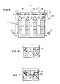
- each of solder balls 40, 42, 46, etc. is held within upper and lower limits.
- the dimension between the exposed tips of conductors 10, 12, and 14 and the upper surface of polymer layer should be approximately equal to the lower limit height dimension of the solder balls. Should a solder ball not connect to a conductor, then it is known that the ball is out of limits, causing the chip to be rejected.
- Interconnect module 16 as shown in Fig. 5, is mounted in an alignment fixture 30.
- the upper portion of alignment fixture 30 holds a polymeric sheet 32 which is provided with openings aligned with the openings previously made in polymer layer 20.
- the thickness of sheet 32 maybe selected to control the depth of indentation into each of the solder balls.
- a pair of adjustment screws 34 and 36 enable module 16 to be moved so that the openings in layer 20 are aligned with the openings in sheet 32.
- a chip 38 having a plurality of solder balls 40, 42, and 46 is emplaced over polymeric sheet 32 so that the solder balls extend therethrough.
- the upper surface of chip 38 is pressed downwardly until each of balls 40, 42, and 46 makes contact with the upper surfaces of conductors 10, 12, and 14.
- Sufficient force is applied (as schematically indicated by arrow 50) to chip 38 to cause conductors 10, 12, and 14 to indent each of solder balls 40, 42, and 46, thereby enabling good electrical contact to be established.
- Fig. 6 an expanded view is shown of solder ball 46 and conductor 14 is after sufficient pressure has been exerted on chip 38 to cause conductor 14 to indent ball 46.
- the above-described interconnection module provides a number of advantages. No permanent joining between the chip and the test module is necessary; it enables the simultaneous testing of many chips; it is applicable for both functional tests and burn-in tests using a single interconnect module; the chip is self-aligned and is mechanically held in place during the test operation; and the indented solder balls may be reformed by a simple reflow operation subsequent to test, if necessary.
Landscapes
- Physics & Mathematics (AREA)
- General Physics & Mathematics (AREA)
- Engineering & Computer Science (AREA)
- Computer Hardware Design (AREA)
- Microelectronics & Electronic Packaging (AREA)
- Testing Of Individual Semiconductor Devices (AREA)
- Measuring Leads Or Probes (AREA)
Applications Claiming Priority (2)
| Application Number | Priority Date | Filing Date | Title |
|---|---|---|---|
| US485016 | 1990-02-23 | ||
| US07/485,016 US4975079A (en) | 1990-02-23 | 1990-02-23 | Connector assembly for chip testing |
Publications (3)
| Publication Number | Publication Date |
|---|---|
| EP0453716A2 true EP0453716A2 (de) | 1991-10-30 |
| EP0453716A3 EP0453716A3 (en) | 1992-07-01 |
| EP0453716B1 EP0453716B1 (de) | 1995-12-06 |
Family
ID=23926601
Family Applications (1)
| Application Number | Title | Priority Date | Filing Date |
|---|---|---|---|
| EP91101647A Expired - Lifetime EP0453716B1 (de) | 1990-02-23 | 1991-02-07 | Anschlussanordnung zum Testen eines Chips |
Country Status (4)
| Country | Link |
|---|---|
| US (1) | US4975079A (de) |
| EP (1) | EP0453716B1 (de) |
| JP (1) | JPH0619371B2 (de) |
| DE (1) | DE69115106D1 (de) |
Cited By (5)
| Publication number | Priority date | Publication date | Assignee | Title |
|---|---|---|---|---|
| EP0764352A1 (de) * | 1994-06-07 | 1997-03-26 | Tessera, Inc. | Mikroelektronische kontakte und zusammenbauten |
| WO1998027590A1 (en) * | 1996-12-19 | 1998-06-25 | Telefonaktiebolaget Lm Ericsson (Publ) | Bumps in grooves for elastic positioning |
| EP1014096A2 (de) * | 1998-12-21 | 2000-06-28 | Shinko Electric Industries Co. Ltd. | Substrat und Verfahren zur Prüfung |
| US6205660B1 (en) | 1994-06-07 | 2001-03-27 | Tessera, Inc. | Method of making an electronic contact |
| US8033838B2 (en) | 1996-02-21 | 2011-10-11 | Formfactor, Inc. | Microelectronic contact structure |
Families Citing this family (106)
| Publication number | Priority date | Publication date | Assignee | Title |
|---|---|---|---|---|
| US5917707A (en) | 1993-11-16 | 1999-06-29 | Formfactor, Inc. | Flexible contact structure with an electrically conductive shell |
| JP2798188B2 (ja) * | 1991-01-30 | 1998-09-17 | 松下電子工業株式会社 | 半導体素子の試験装置 |
| US5237269A (en) * | 1991-03-27 | 1993-08-17 | International Business Machines Corporation | Connections between circuit chips and a temporary carrier for use in burn-in tests |
| US5279711A (en) * | 1991-07-01 | 1994-01-18 | International Business Machines Corporation | Chip attach and sealing method |
| US5338208A (en) * | 1992-02-04 | 1994-08-16 | International Business Machines Corporation | High density electronic connector and method of assembly |
| US5289631A (en) * | 1992-03-04 | 1994-03-01 | Mcnc | Method for testing, burn-in, and/or programming of integrated circuit chips |
| JP3302059B2 (ja) * | 1992-10-30 | 2002-07-15 | ジェイエスアール株式会社 | バーン・イン・テスト用治具 |
| JPH0677467B2 (ja) * | 1992-12-25 | 1994-09-28 | 山一電機株式会社 | Icソケット |
| US20020053734A1 (en) | 1993-11-16 | 2002-05-09 | Formfactor, Inc. | Probe card assembly and kit, and methods of making same |
| US5820014A (en) | 1993-11-16 | 1998-10-13 | Form Factor, Inc. | Solder preforms |
| US7064566B2 (en) * | 1993-11-16 | 2006-06-20 | Formfactor, Inc. | Probe card assembly and kit |
| US5500607A (en) * | 1993-12-22 | 1996-03-19 | International Business Machines Corporation | Probe-oxide-semiconductor method and apparatus for measuring oxide charge on a semiconductor wafer |
| US5800184A (en) * | 1994-03-08 | 1998-09-01 | International Business Machines Corporation | High density electrical interconnect apparatus and method |
| JP3578232B2 (ja) * | 1994-04-07 | 2004-10-20 | インターナショナル・ビジネス・マシーンズ・コーポレーション | 電気接点形成方法、該電気接点を含むプローブ構造および装置 |
| US5802699A (en) * | 1994-06-07 | 1998-09-08 | Tessera, Inc. | Methods of assembling microelectronic assembly with socket for engaging bump leads |
| US5447264A (en) * | 1994-07-01 | 1995-09-05 | Mcnc | Recessed via apparatus for testing, burn-in, and/or programming of integrated circuit chips, and for placing solder bumps thereon |
| US5983492A (en) * | 1996-11-27 | 1999-11-16 | Tessera, Inc. | Low profile socket for microelectronic components and method for making the same |
| US6826827B1 (en) | 1994-12-29 | 2004-12-07 | Tessera, Inc. | Forming conductive posts by selective removal of conductive material |
| JP3260253B2 (ja) * | 1995-01-06 | 2002-02-25 | 松下電器産業株式会社 | 半導体装置の検査方法と検査用導電性接着剤 |
| TW308724B (de) * | 1995-07-03 | 1997-06-21 | Motorola Inc | |
| US5600257A (en) * | 1995-08-09 | 1997-02-04 | International Business Machines Corporation | Semiconductor wafer test and burn-in |
| US5810609A (en) | 1995-08-28 | 1998-09-22 | Tessera, Inc. | Socket for engaging bump leads on a microelectronic device and methods therefor |
| US6448169B1 (en) * | 1995-12-21 | 2002-09-10 | International Business Machines Corporation | Apparatus and method for use in manufacturing semiconductor devices |
| US5994152A (en) | 1996-02-21 | 1999-11-30 | Formfactor, Inc. | Fabricating interconnects and tips using sacrificial substrates |
| SG71046A1 (en) | 1996-10-10 | 2000-03-21 | Connector Systems Tech Nv | High density connector and method of manufacture |
| US5764486A (en) * | 1996-10-10 | 1998-06-09 | Hewlett Packard Company | Cost effective structure and method for interconnecting a flip chip with a substrate |
| US6048744A (en) | 1997-09-15 | 2000-04-11 | Micron Technology, Inc. | Integrated circuit package alignment feature |
| US6200143B1 (en) | 1998-01-09 | 2001-03-13 | Tessera, Inc. | Low insertion force connector for microelectronic elements |
| US6337575B1 (en) | 1998-12-23 | 2002-01-08 | Micron Technology, Inc. | Methods of testing integrated circuitry, methods of forming tester substrates, and circuitry testing substrates |
| US6429030B1 (en) | 1999-02-08 | 2002-08-06 | Motorola, Inc. | Method for testing a semiconductor die using wells |
| US6464513B1 (en) | 2000-01-05 | 2002-10-15 | Micron Technology, Inc. | Adapter for non-permanently connecting integrated circuit devices to multi-chip modules and method of using same |
| US6407566B1 (en) | 2000-04-06 | 2002-06-18 | Micron Technology, Inc. | Test module for multi-chip module simulation testing of integrated circuit packages |
| US6866521B1 (en) | 2000-09-14 | 2005-03-15 | Fci Americas Technology, Inc. | High density connector |
| US7045889B2 (en) | 2001-08-21 | 2006-05-16 | Micron Technology, Inc. | Device for establishing non-permanent electrical connection between an integrated circuit device lead element and a substrate |
| US7049693B2 (en) | 2001-08-29 | 2006-05-23 | Micron Technology, Inc. | Electrical contact array for substrate assemblies |
| US6991960B2 (en) | 2001-08-30 | 2006-01-31 | Micron Technology, Inc. | Method of semiconductor device package alignment and method of testing |
| US7462936B2 (en) * | 2003-10-06 | 2008-12-09 | Tessera, Inc. | Formation of circuitry with modification of feature height |
| US8641913B2 (en) * | 2003-10-06 | 2014-02-04 | Tessera, Inc. | Fine pitch microcontacts and method for forming thereof |
| US7495179B2 (en) * | 2003-10-06 | 2009-02-24 | Tessera, Inc. | Components with posts and pads |
| US8207604B2 (en) * | 2003-12-30 | 2012-06-26 | Tessera, Inc. | Microelectronic package comprising offset conductive posts on compliant layer |
| US7709968B2 (en) * | 2003-12-30 | 2010-05-04 | Tessera, Inc. | Micro pin grid array with pin motion isolation |
| US7176043B2 (en) | 2003-12-30 | 2007-02-13 | Tessera, Inc. | Microelectronic packages and methods therefor |
| US7453157B2 (en) | 2004-06-25 | 2008-11-18 | Tessera, Inc. | Microelectronic packages and methods therefor |
| US20060027899A1 (en) * | 2004-06-25 | 2006-02-09 | Tessera, Inc. | Structure with spherical contact pins |
| US8525314B2 (en) | 2004-11-03 | 2013-09-03 | Tessera, Inc. | Stacked packaging improvements |
| US7939934B2 (en) * | 2005-03-16 | 2011-05-10 | Tessera, Inc. | Microelectronic packages and methods therefor |
| US8058101B2 (en) * | 2005-12-23 | 2011-11-15 | Tessera, Inc. | Microelectronic packages and methods therefor |
| US8067267B2 (en) * | 2005-12-23 | 2011-11-29 | Tessera, Inc. | Microelectronic assemblies having very fine pitch stacking |
| US7545029B2 (en) | 2006-08-18 | 2009-06-09 | Tessera, Inc. | Stack microelectronic assemblies |
| US20080150101A1 (en) * | 2006-12-20 | 2008-06-26 | Tessera, Inc. | Microelectronic packages having improved input/output connections and methods therefor |
| EP2637202A3 (de) | 2007-09-28 | 2014-03-12 | Tessera, Inc. | Flip-Chip-Verbindung mit zu durch Ätzten ausgebildeten Säulen auf einem Substrat mittels Schmelzmetal verbundenen durch Ätzten ausgebildeten Säulen auf einem mikroelektronischen Bauelement und entsprechendes Herstellungsverfahren |
| US20100044860A1 (en) * | 2008-08-21 | 2010-02-25 | Tessera Interconnect Materials, Inc. | Microelectronic substrate or element having conductive pads and metal posts joined thereto using bond layer |
| US8330272B2 (en) | 2010-07-08 | 2012-12-11 | Tessera, Inc. | Microelectronic packages with dual or multiple-etched flip-chip connectors |
| US9159708B2 (en) | 2010-07-19 | 2015-10-13 | Tessera, Inc. | Stackable molded microelectronic packages with area array unit connectors |
| US8482111B2 (en) | 2010-07-19 | 2013-07-09 | Tessera, Inc. | Stackable molded microelectronic packages |
| US8580607B2 (en) | 2010-07-27 | 2013-11-12 | Tessera, Inc. | Microelectronic packages with nanoparticle joining |
| KR101075241B1 (ko) | 2010-11-15 | 2011-11-01 | 테세라, 인코포레이티드 | 유전체 부재에 단자를 구비하는 마이크로전자 패키지 |
| US8853558B2 (en) | 2010-12-10 | 2014-10-07 | Tessera, Inc. | Interconnect structure |
| US20120146206A1 (en) | 2010-12-13 | 2012-06-14 | Tessera Research Llc | Pin attachment |
| US9137903B2 (en) | 2010-12-21 | 2015-09-15 | Tessera, Inc. | Semiconductor chip assembly and method for making same |
| US8618659B2 (en) | 2011-05-03 | 2013-12-31 | Tessera, Inc. | Package-on-package assembly with wire bonds to encapsulation surface |
| KR101128063B1 (ko) | 2011-05-03 | 2012-04-23 | 테세라, 인코포레이티드 | 캡슐화 층의 표면에 와이어 본드를 구비하는 패키지 적층형 어셈블리 |
| US8872318B2 (en) | 2011-08-24 | 2014-10-28 | Tessera, Inc. | Through interposer wire bond using low CTE interposer with coarse slot apertures |
| US8404520B1 (en) | 2011-10-17 | 2013-03-26 | Invensas Corporation | Package-on-package assembly with wire bond vias |
| US8946757B2 (en) | 2012-02-17 | 2015-02-03 | Invensas Corporation | Heat spreading substrate with embedded interconnects |
| US9349706B2 (en) | 2012-02-24 | 2016-05-24 | Invensas Corporation | Method for package-on-package assembly with wire bonds to encapsulation surface |
| US8372741B1 (en) | 2012-02-24 | 2013-02-12 | Invensas Corporation | Method for package-on-package assembly with wire bonds to encapsulation surface |
| US8835228B2 (en) | 2012-05-22 | 2014-09-16 | Invensas Corporation | Substrate-less stackable package with wire-bond interconnect |
| US9391008B2 (en) | 2012-07-31 | 2016-07-12 | Invensas Corporation | Reconstituted wafer-level package DRAM |
| US9502390B2 (en) | 2012-08-03 | 2016-11-22 | Invensas Corporation | BVA interposer |
| KR20140035590A (ko) * | 2012-09-14 | 2014-03-24 | 삼성전자주식회사 | 전자장치와 그 제어방법 |
| US8975738B2 (en) | 2012-11-12 | 2015-03-10 | Invensas Corporation | Structure for microelectronic packaging with terminals on dielectric mass |
| US8878353B2 (en) | 2012-12-20 | 2014-11-04 | Invensas Corporation | Structure for microelectronic packaging with bond elements to encapsulation surface |
| US9136254B2 (en) | 2013-02-01 | 2015-09-15 | Invensas Corporation | Microelectronic package having wire bond vias and stiffening layer |
| US8883563B1 (en) | 2013-07-15 | 2014-11-11 | Invensas Corporation | Fabrication of microelectronic assemblies having stack terminals coupled by connectors extending through encapsulation |
| US9034696B2 (en) | 2013-07-15 | 2015-05-19 | Invensas Corporation | Microelectronic assemblies having reinforcing collars on connectors extending through encapsulation |
| US9023691B2 (en) | 2013-07-15 | 2015-05-05 | Invensas Corporation | Microelectronic assemblies with stack terminals coupled by connectors extending through encapsulation |
| US9167710B2 (en) | 2013-08-07 | 2015-10-20 | Invensas Corporation | Embedded packaging with preformed vias |
| US9685365B2 (en) | 2013-08-08 | 2017-06-20 | Invensas Corporation | Method of forming a wire bond having a free end |
| US20150076714A1 (en) | 2013-09-16 | 2015-03-19 | Invensas Corporation | Microelectronic element with bond elements to encapsulation surface |
| US9087815B2 (en) | 2013-11-12 | 2015-07-21 | Invensas Corporation | Off substrate kinking of bond wire |
| US9082753B2 (en) | 2013-11-12 | 2015-07-14 | Invensas Corporation | Severing bond wire by kinking and twisting |
| US9379074B2 (en) | 2013-11-22 | 2016-06-28 | Invensas Corporation | Die stacks with one or more bond via arrays of wire bond wires and with one or more arrays of bump interconnects |
| US9263394B2 (en) | 2013-11-22 | 2016-02-16 | Invensas Corporation | Multiple bond via arrays of different wire heights on a same substrate |
| US9583456B2 (en) | 2013-11-22 | 2017-02-28 | Invensas Corporation | Multiple bond via arrays of different wire heights on a same substrate |
| US9583411B2 (en) | 2014-01-17 | 2017-02-28 | Invensas Corporation | Fine pitch BVA using reconstituted wafer with area array accessible for testing |
| US9214454B2 (en) | 2014-03-31 | 2015-12-15 | Invensas Corporation | Batch process fabrication of package-on-package microelectronic assemblies |
| US10381326B2 (en) | 2014-05-28 | 2019-08-13 | Invensas Corporation | Structure and method for integrated circuits packaging with increased density |
| US9646917B2 (en) | 2014-05-29 | 2017-05-09 | Invensas Corporation | Low CTE component with wire bond interconnects |
| US9412714B2 (en) | 2014-05-30 | 2016-08-09 | Invensas Corporation | Wire bond support structure and microelectronic package including wire bonds therefrom |
| US9735084B2 (en) | 2014-12-11 | 2017-08-15 | Invensas Corporation | Bond via array for thermal conductivity |
| US9888579B2 (en) | 2015-03-05 | 2018-02-06 | Invensas Corporation | Pressing of wire bond wire tips to provide bent-over tips |
| US9502372B1 (en) | 2015-04-30 | 2016-11-22 | Invensas Corporation | Wafer-level packaging using wire bond wires in place of a redistribution layer |
| US9761554B2 (en) | 2015-05-07 | 2017-09-12 | Invensas Corporation | Ball bonding metal wire bond wires to metal pads |
| US10886250B2 (en) | 2015-07-10 | 2021-01-05 | Invensas Corporation | Structures and methods for low temperature bonding using nanoparticles |
| US9633971B2 (en) | 2015-07-10 | 2017-04-25 | Invensas Corporation | Structures and methods for low temperature bonding using nanoparticles |
| US10490528B2 (en) | 2015-10-12 | 2019-11-26 | Invensas Corporation | Embedded wire bond wires |
| US9490222B1 (en) | 2015-10-12 | 2016-11-08 | Invensas Corporation | Wire bond wires for interference shielding |
| US10332854B2 (en) | 2015-10-23 | 2019-06-25 | Invensas Corporation | Anchoring structure of fine pitch bva |
| US10181457B2 (en) | 2015-10-26 | 2019-01-15 | Invensas Corporation | Microelectronic package for wafer-level chip scale packaging with fan-out |
| US10043779B2 (en) | 2015-11-17 | 2018-08-07 | Invensas Corporation | Packaged microelectronic device for a package-on-package device |
| US9659848B1 (en) | 2015-11-18 | 2017-05-23 | Invensas Corporation | Stiffened wires for offset BVA |
| US9984992B2 (en) | 2015-12-30 | 2018-05-29 | Invensas Corporation | Embedded wire bond wires for vertical integration with separate surface mount and wire bond mounting surfaces |
| US9935075B2 (en) | 2016-07-29 | 2018-04-03 | Invensas Corporation | Wire bonding method and apparatus for electromagnetic interference shielding |
| TWI822659B (zh) | 2016-10-27 | 2023-11-21 | 美商艾德亞半導體科技有限責任公司 | 用於低溫接合的結構和方法 |
| US10299368B2 (en) | 2016-12-21 | 2019-05-21 | Invensas Corporation | Surface integrated waveguides and circuit structures therefor |
Citations (2)
| Publication number | Priority date | Publication date | Assignee | Title |
|---|---|---|---|---|
| DE3151933A1 (de) * | 1981-12-30 | 1983-07-14 | Institut Kolloidnoj Chimii i Chimii Vody imeni A.V. Dumanskogo Akademii Nauk Ukrainskoj SSR, Kiev | Elektrischer verbinder |
| EP0153990A1 (de) * | 1983-09-30 | 1985-09-11 | Siemens Aktiengesellschaft | Flachbaugruppe |
Family Cites Families (3)
| Publication number | Priority date | Publication date | Assignee | Title |
|---|---|---|---|---|
| US3680037A (en) * | 1970-11-05 | 1972-07-25 | Tech Wire Prod Inc | Electrical interconnector |
| GB1387587A (en) * | 1971-07-22 | 1975-03-19 | Plessey Co Ltd | Electrical interconnectors and connector assemblies |
| US4373778A (en) * | 1980-12-30 | 1983-02-15 | International Business Machines Corporation | Connector implemented with fiber optic means and site therein for integrated circuit chips |
-
1990
- 1990-02-23 US US07/485,016 patent/US4975079A/en not_active Expired - Fee Related
-
1991
- 1991-02-07 EP EP91101647A patent/EP0453716B1/de not_active Expired - Lifetime
- 1991-02-07 DE DE69115106T patent/DE69115106D1/de not_active Expired - Lifetime
- 1991-02-18 JP JP3044112A patent/JPH0619371B2/ja not_active Expired - Lifetime
Patent Citations (2)
| Publication number | Priority date | Publication date | Assignee | Title |
|---|---|---|---|---|
| DE3151933A1 (de) * | 1981-12-30 | 1983-07-14 | Institut Kolloidnoj Chimii i Chimii Vody imeni A.V. Dumanskogo Akademii Nauk Ukrainskoj SSR, Kiev | Elektrischer verbinder |
| EP0153990A1 (de) * | 1983-09-30 | 1985-09-11 | Siemens Aktiengesellschaft | Flachbaugruppe |
Non-Patent Citations (3)
| Title |
|---|
| IBM TECHNICAL DISCLOSURE BULLETIN. vol. 19, no. 2, July 1976, NEW YORK US page 467; BARKHUFF & STRAUS: 'MINICONTACT PROBE FOR TESTING CHIPS' * |
| IBM TECHNICAL DISCLOSURE BULLETIN. vol. 21, no. 11, April 1979, NEW YORK US pages 4511 - 4512; BYRNES ET AL.: 'PAD DEFORMATION CONTACTOR' * |
| IBM TECHNICAL DISCLOSURE BULLETIN. vol. 27, no. 2, July 1984, NEW YORK US page 1355; BEAMAN: 'LARGE FORMAT SUBSTRATE CONCEPT' * |
Cited By (10)
| Publication number | Priority date | Publication date | Assignee | Title |
|---|---|---|---|---|
| EP0764352A1 (de) * | 1994-06-07 | 1997-03-26 | Tessera, Inc. | Mikroelektronische kontakte und zusammenbauten |
| EP0764352A4 (de) * | 1994-06-07 | 2000-03-15 | Tessera Inc | Mikroelektronische kontakte und zusammenbauten |
| US6205660B1 (en) | 1994-06-07 | 2001-03-27 | Tessera, Inc. | Method of making an electronic contact |
| US6938338B2 (en) | 1994-06-07 | 2005-09-06 | Tessera, Inc. | Method of making an electronic contact |
| US8033838B2 (en) | 1996-02-21 | 2011-10-11 | Formfactor, Inc. | Microelectronic contact structure |
| WO1998027590A1 (en) * | 1996-12-19 | 1998-06-25 | Telefonaktiebolaget Lm Ericsson (Publ) | Bumps in grooves for elastic positioning |
| US6188138B1 (en) | 1996-12-19 | 2001-02-13 | Telefonaktiebolaget Lm Ericsson (Pub) | Bumps in grooves for elastic positioning |
| EP1014096A2 (de) * | 1998-12-21 | 2000-06-28 | Shinko Electric Industries Co. Ltd. | Substrat und Verfahren zur Prüfung |
| EP1014096A3 (de) * | 1998-12-21 | 2001-06-27 | Shinko Electric Industries Co. Ltd. | Substrat und Verfahren zur Prüfung |
| US6404214B1 (en) | 1998-12-21 | 2002-06-11 | Shinko Electric Industries Co., Ltd. | Substrate for inspecting electronic device, method of manufacturing substrate, and method of inspecting electronic device |
Also Published As
| Publication number | Publication date |
|---|---|
| EP0453716A3 (en) | 1992-07-01 |
| JPH04215069A (ja) | 1992-08-05 |
| EP0453716B1 (de) | 1995-12-06 |
| JPH0619371B2 (ja) | 1994-03-16 |
| US4975079A (en) | 1990-12-04 |
| DE69115106D1 (de) | 1996-01-18 |
Similar Documents
| Publication | Publication Date | Title |
|---|---|---|
| US4975079A (en) | Connector assembly for chip testing | |
| US6642625B2 (en) | Sockets for “springed” semiconductor devices | |
| US7002362B2 (en) | Test system for bumped semiconductor components | |
| US6400169B1 (en) | Test socket with interposer for testing semiconductor components having contact balls | |
| EP1092338B1 (de) | Zusammenbau von elektronischen komponenten mittels federpackungen | |
| US6493932B1 (en) | Lidless socket and method of making same | |
| US5410807A (en) | High density electronic connector and method of assembly | |
| US6474997B1 (en) | Contact sheet | |
| KR100408948B1 (ko) | 전자부품을 회로기판에 장착하는 방법 | |
| US5828226A (en) | Probe card assembly for high density integrated circuits | |
| US5810609A (en) | Socket for engaging bump leads on a microelectronic device and methods therefor | |
| US6329827B1 (en) | High density cantilevered probe for electronic devices | |
| US20010024892A1 (en) | Contact sheet | |
| US6722032B2 (en) | Method of forming a structure for electronic devices contact locations | |
| US20080030215A1 (en) | High density cantilevered probe for electronic devices | |
| US6256879B1 (en) | Compression connector | |
| USRE36442E (en) | Adapter which emulates ball grid array packages | |
| US20010040464A1 (en) | Electric contact device for testing semiconductor device | |
| US4870356A (en) | Multi-component test fixture | |
| KR100707044B1 (ko) | 집적회로 웨이퍼 프로브카드 조립체의 구조물 및 그 제조방법 | |
| US6819127B1 (en) | Method for testing semiconductor components using interposer | |
| US20020076957A1 (en) | Contact elements for surface mounting of burn-in socket | |
| JP4209696B2 (ja) | 電気的接続装置 | |
| US6168976B1 (en) | Socketable BGA package | |
| US6182883B1 (en) | Method and apparatus for precisely registering solder paste in a printed circuit board repair operation |
Legal Events
| Date | Code | Title | Description |
|---|---|---|---|
| PUAI | Public reference made under article 153(3) epc to a published international application that has entered the european phase |
Free format text: ORIGINAL CODE: 0009012 |
|
| AK | Designated contracting states |
Kind code of ref document: A2 Designated state(s): DE FR GB |
|
| 17P | Request for examination filed |
Effective date: 19911211 |
|
| PUAL | Search report despatched |
Free format text: ORIGINAL CODE: 0009013 |
|
| AK | Designated contracting states |
Kind code of ref document: A3 Designated state(s): DE FR GB |
|
| 17Q | First examination report despatched |
Effective date: 19931210 |
|
| GRAA | (expected) grant |
Free format text: ORIGINAL CODE: 0009210 |
|
| AK | Designated contracting states |
Kind code of ref document: B1 Designated state(s): DE FR GB |
|
| REF | Corresponds to: |
Ref document number: 69115106 Country of ref document: DE Date of ref document: 19960118 |
|
| PGFP | Annual fee paid to national office [announced via postgrant information from national office to epo] |
Ref country code: GB Payment date: 19960126 Year of fee payment: 6 |
|
| PGFP | Annual fee paid to national office [announced via postgrant information from national office to epo] |
Ref country code: FR Payment date: 19960131 Year of fee payment: 6 |
|
| PG25 | Lapsed in a contracting state [announced via postgrant information from national office to epo] |
Ref country code: DE Effective date: 19960307 |
|
| ET | Fr: translation filed | ||
| PLBE | No opposition filed within time limit |
Free format text: ORIGINAL CODE: 0009261 |
|
| STAA | Information on the status of an ep patent application or granted ep patent |
Free format text: STATUS: NO OPPOSITION FILED WITHIN TIME LIMIT |
|
| 26N | No opposition filed | ||
| PG25 | Lapsed in a contracting state [announced via postgrant information from national office to epo] |
Ref country code: GB Effective date: 19970207 |
|
| GBPC | Gb: european patent ceased through non-payment of renewal fee |
Effective date: 19970207 |
|
| PG25 | Lapsed in a contracting state [announced via postgrant information from national office to epo] |
Ref country code: FR Effective date: 19971030 |
|
| REG | Reference to a national code |
Ref country code: FR Ref legal event code: ST |