EP0453424B1 - Integrierte Schaltungsanordnung mit Abschirmungsvorrichtung und Verfahren zu ihrer Herstellung - Google Patents
Integrierte Schaltungsanordnung mit Abschirmungsvorrichtung und Verfahren zu ihrer Herstellung Download PDFInfo
- Publication number
- EP0453424B1 EP0453424B1 EP91850073A EP91850073A EP0453424B1 EP 0453424 B1 EP0453424 B1 EP 0453424B1 EP 91850073 A EP91850073 A EP 91850073A EP 91850073 A EP91850073 A EP 91850073A EP 0453424 B1 EP0453424 B1 EP 0453424B1
- Authority
- EP
- European Patent Office
- Prior art keywords
- layer
- semiconductor
- polycrystalline
- ions
- integrated circuit
- Prior art date
- Legal status (The legal status is an assumption and is not a legal conclusion. Google has not performed a legal analysis and makes no representation as to the accuracy of the status listed.)
- Expired - Lifetime
Links
Images

Classifications
-
- H—ELECTRICITY
- H10—SEMICONDUCTOR DEVICES; ELECTRIC SOLID-STATE DEVICES NOT OTHERWISE PROVIDED FOR
- H10W—GENERIC PACKAGES, INTERCONNECTIONS, CONNECTORS OR OTHER CONSTRUCTIONAL DETAILS OF DEVICES COVERED BY CLASS H10
- H10W42/00—Arrangements for protection of devices
-
- H—ELECTRICITY
- H10—SEMICONDUCTOR DEVICES; ELECTRIC SOLID-STATE DEVICES NOT OTHERWISE PROVIDED FOR
- H10D—INORGANIC ELECTRIC SEMICONDUCTOR DEVICES
- H10D84/00—Integrated devices formed in or on semiconductor substrates that comprise only semiconducting layers, e.g. on Si wafers or on GaAs-on-Si wafers
- H10D84/201—Integrated devices formed in or on semiconductor substrates that comprise only semiconducting layers, e.g. on Si wafers or on GaAs-on-Si wafers characterised by the integration of only components covered by H10D1/00 or H10D8/00, e.g. RLC circuits
- H10D84/204—Integrated devices formed in or on semiconductor substrates that comprise only semiconducting layers, e.g. on Si wafers or on GaAs-on-Si wafers characterised by the integration of only components covered by H10D1/00 or H10D8/00, e.g. RLC circuits of combinations of diodes or capacitors or resistors
- H10D84/206—Integrated devices formed in or on semiconductor substrates that comprise only semiconducting layers, e.g. on Si wafers or on GaAs-on-Si wafers characterised by the integration of only components covered by H10D1/00 or H10D8/00, e.g. RLC circuits of combinations of diodes or capacitors or resistors of combinations of capacitors and resistors
-
- H—ELECTRICITY
- H10—SEMICONDUCTOR DEVICES; ELECTRIC SOLID-STATE DEVICES NOT OTHERWISE PROVIDED FOR
- H10W—GENERIC PACKAGES, INTERCONNECTIONS, CONNECTORS OR OTHER CONSTRUCTIONAL DETAILS OF DEVICES COVERED BY CLASS H10
- H10W20/00—Interconnections in chips, wafers or substrates
- H10W20/40—Interconnections external to wafers or substrates, e.g. back-end-of-line [BEOL] metallisations or vias connecting to gate electrodes
- H10W20/41—Interconnections external to wafers or substrates, e.g. back-end-of-line [BEOL] metallisations or vias connecting to gate electrodes characterised by their conductive parts
- H10W20/44—Conductive materials thereof
- H10W20/4451—Semiconductor materials, e.g. polysilicon
Definitions
- the present invention relates to an integrated bipolar transistor circuit arrangement comprising
- the invention also relates to a method for producing the arrangement.
- parasite-MOS transistor Metal Oxide Semiconductor
- the integrated circuit is built on a semiconductor substrate and includes an epitaxial layer in which the base regions are diffused. The base regions are spaced so wide apart as to normally prevent the two bipolar transistors from disturbing one another.
- Several other layers are found on the epitaxial layer, for instance an insulating first oxide layer which lies immediately on the epitaxial layer, electrical connections and an electrically insulating protective layer which forms the uppermost layer of the composite structure.
- This protective layer may become covered with an undesirable film of moisture, which is electrically conductive and connected, for instance, to a terminal voltage of the integrated circuit.
- the moisture film functions as a gate and lies on the potential of the terminal voltage and attracts charges in the epitaxial layer between the base regions, so-called inversion, therewith creating the aforesaid parasite-MOS transistor.
- inversion In order for inversion to take place, it is necessary for the potential of the moisture film to exceed a field threshold voltage.
- parasite-MOS transistors can be avoided relatively easily in the case of integrated circuits which are intended for low voltages, for instance memory circuits in computers with terminal voltages about 5 volts. In such integrated circuits, inversion can be counteracted in a known manner, by raising the field threshold voltage with the aid of an additional diffusion or implantation.
- this method requires wide spacing between the diffusion which raises the threshold voltage and, for instance, a base diffusion, in order not to degrade the breakdown voltage of the transistor.
- Another known alternative involves the use of a metal screen.
- the metal screen is connected to the potential of the epitaxial layer and prevents parasitic inversion from taking place beneath the screen.
- the drawback with this method lies in the difficulty experienced in running the metal conductors and connecting these conductors to peripheral components.
- the conductor layout and the screens are effected with one and the same metal layer and it is difficult to avoid short circuiting.
- One known solution involves the use of two metal layers, one for the screens and one for the conductor layout.
- the oxide layer which needs to be deposited on the first metal layer as an electrical insulation against the second metal layer constitutes a particular problem.
- the metallization cannot withstand high temperatures and it is necessary for the oxide layer to cover the topography of the disk uniformly in order to enable a good second metallization to be achieved. The lower the highest temperature available, the more difficult this is to achieve.
- the first oxide layer is a polycrystalline layer around the base of a transistor, this layer forming a screen which prevents an electrical breakdown at the base edges.
- the polycrystalline layer and the metal screen are applied in separate process steps with the aid of separate masks and these process steps are relatively expensive.
- One such polycrystalline base screen is found described in more detail in Revue De Physique Appliquée, Tome 13, Décumble 1978, M. Roche: "An Advanced Processing Technology for High Voltage Bipolar IC's". In this case, the screen is connected through a metallic connection to a potential which is positive in relation to the potential of the epitaxial layer.
- Another example of a polycrystalline layer is found described in IEEE Transactions on Electron Devices, Vol.
- an integrated circuit screen arrangement comprising a field effect transistor device in a semiconductor layer and an insulating semiconductor oxide layer on the semiconductor layer. Embedded in the oxide layer are heavily doped polycrystalline semiconductor layers, electrically connected to the semiconductor layer. The polycrystalline layers form a shield, preventing parasitic inversion layers to occur in the semiconductor layer.
- the screen between the base regions, the electrical connection to the epitaxial layer and the electrical connection between the screen and the epitaxial-layer connection comprises heavily doped, polycrystalline semiconductor layers on the insulating oxide layer.
- the oxide layer also carries electrical resistors and capacitor coatings which consist of doped polycrystalline layers.
- the polycrystalline layers can be applied in a few mutually common method steps and are relatively resistant to temperature. This temperature resistance enables the method to be simplified when the polycrystalline layers are coated with insulating semiconductor layers.
- the invention has the characterizing features set forth in the following Claims.
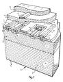
- FIG. 1 is perspective, cross-sectional view of a preferred embodiment of the invention.
- An integrated circuit 1 includes, in a known manner, a semiconductive substrate 2, which in the illustrated embodiment is a weakly positive p ⁇ doped silicon plate.
- the silicon plate carries a weakly negative n ⁇ doped epitaxial silicon layer 3.
- Located in the surface of the epitaxial layer are two positively doped and mutually spaced component regions 4.
- the component regions form two separate bipolar transistors, which have not been shown in detail in the Figure for the sake of clarity.
- Located on the epitaxial layer 3 is a first insulating silicon-dioxide layer 5 which presents cut-out 6 through which electric connection with the epitaxial layer 3 are made.
- the first silicon-dioxide layer 5 carries layers of polycrystalline silicon, which in accordance with the invention include an electric contact layer 7, a screen layer 8 and a connecting layer 9.
- the electrical contact layer 7 extends into the cut-out 6 and is formed on the oxide layer 5 in the close proximity of the cut-out.
- the screen layer 8 extends in a region which is located between the base regions 4 and is connected electrically to the electrical contact layer 7 through the connecting layer 9. This layer extends between the layer 7 and the screen layer 8 in a region which is spaced from the base regions 4, as shown in the Figure.
- the three polycrystalline layers 7, 8 and 9 are heavily negatively n+-doped and are electrically conductive.
- the heavy n+-doping extends down to the epitaxial layer 3 through the cut-out 6 and down to the regions 10, which form an electrical connection with the emitters of the bipolar transistors and also form a means for connecting the screen layer 8 electrically to the epitaxial layer 3.
- the first silicon-dioxide layer 5 and the polycrystalline layers 7, 8 and 9 are covered by a second silicon-dioxide layer 11. This layer forms an electrical insulation against other electrical conductors in the integrated circuit 1, for instance a metallic conductor 12.
- the second silicon-dioxide layer 11 is covered by a protective layer 13, for instance a silicon-dioxide layer.
- the surface of the protective layer 13 will become electrically conductive, for instance by the formation of a film of moisture thereon.
- This film may possibly be connected with a voltage connected to the integrated circuit 1, for instance a collector voltage V c for the bipolar transistors of a magnitude of -90 volts.
- the connection to the moisture film is able to extend via the edges of the integrated circuit or via the capsule in which the circuit is encapsulated.
- the film of moisture present on the surface of the protective layer 13 assumes a potential in the proximity of V c and attracts positive charges in the epitaxial layer 3, the aforesaid inversion. This has been marked in Figure 1 with the sign + at the base regions 4.
- the screen layer 8 prevents the attraction of charges beneath this layer, which has the same potential as the epitaxial layer 3.
- a continuous region of positive charges is formed between the base regions 4. This results in the aforesaid undesirable parasite MOS-transistor, which is in its conductive state.
- V c the voltage V c for which the integrated circuit is intended to exceed a threshold voltage for the epitaxial layer 3.
- the epitaxial layer 3 lies on the silicon substrate 2 and carries the insulating silicon-dioxide layer 5.
- the surface of the epitaxial layer carries the component regions 4 and the oxide layer 5 has cut-out 6 formed therein for the electrical contact layers 7.
- the screen layer 8 extends on the oxide layer 5 in the region between said component regions 4.
- the screen layer 8 and the electrical contact layer 7 are mutually connected through the connecting layer 9.
- the oxide layer 5 carries further layers of polycrystalline silicon. of these layers, one is a resistance layer 14 doped with ions of desired polarity to a desired degree of doping and forms an electrical resistor in the integrated circuit 1.
- a capacitor layer 15 is heavily doped and forms the one conductive coating of a first capacitor.
- This capacitor has a second conductive coating which forms a heavily and negatively n+-doped region 16 in the epitaxial layer 3.
- the dielectric 17 of the capacitor consists of silicon dioxide.
- a second capacitor has a conductive coating 18 of heavily doped polycrystalline silicon, a dielectric 19 and a further coating which forms a positively p-doped region in the epitaxial layer 3.
- the polycrystalline layers 7, 8, 9, 14, 15 and 18 form parts of a common polycrystalline layer. This layer is applied to the oxide layer 5 by means of a method described hereinafter with reference to Figures 3-8.
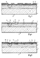
- Figure 3 illustrates the weakly and positively doped silicon substrate 2, on which the weekly negatively doped epitaxial silicon layer 3 is grown in a known manner. Regions in the substrate 2 can be doped prior to growing the epitaxial silicon layer 3, although such forms no part of the present invention and is therefore not shown in the Figures. Regions are heavily doped in the epitaxial layer 3 with the aid of masks, not shown in detail.
- One example in this regard is the region 16, which has been doped heavily negative n+ in order to form a part of a capacitor in the integrated circuit 1.
- the first oxide layer 5, which has a thickness of 900nm (9000 ⁇ ), is applied to the epitaxial layer, for instance by oxidizing said layer on the surface of the epitaxial layer.
- Holes are formed in the oxide layer 5 with the aid of a masking procedure which includes several part stages.
- a layer 20 of photoresistive material is applied to the oxide layer 5, whereafter a photographic component mask 21 is applied on the upper surface of the layer 20.
- This photoresistive layer 20 is exposed and developed in the openings of the mask 21, whereafter the mask and the developed photoresistive 20 are removed and windows 22 are etched in the oxide layer 5.
- the residue of the photoresistive layer 20 is then removed, as illustrated in Figure 4.
- the component regions 4 and the regions 23 and 24 are then doped with positive ions p through the windows 22, either by diffusion or by ion implantation. Other parts of the epitaxial layer 3 are protected against this doping by the oxide layer 5.
- This positive doping is much weaker than the preceding negative doping of the region 16, and the whole of the region 16 remains negatively doped.
- Doping through the windows 22 is effected in an oxidizing atmosphere, such as to grow oxide layers 25 to a thickness of about 300 nm (3000 ⁇ ) on the epitaxial layer 3 in the windows 22 during the doping process. This is illustrated in Figure 4 by broken lines in the windows.
- the cutouts 6 are etched in the oxide layer 5 and also electrical conduct holes 26 are formed through the oxide layer 25 and down to the component regions 4 by a renewed masking process using an etching mask, as illustrated in Figure 5.
- a polycrystalline silicon layer 27 is deposited over the whole of the integrated circuit 1 and this surface is oxidized to form a diffusion-blocking layer 28.
- Windows 29 are opened in the oxide layer 28, by means of a photolithographic masking method, as described above and as illustrated in Figure 6. According to this example, the windows are formed over the capacitor regions 16 and 23 and the component regions 4, and also over the electrical contact layer 7, the screen layer 8 and the connecting layer 9, as illustrated in Figure 1.
- the polycrystalline layer 27 is heavily doped in the windows 29, by diffusion of negative n+-ions. The negative ions penetrate down into the epitaxial layer 3 in those regions in the windows 29 where no oxide layer 5 or 25 is present, i.e. in the cut-outs 6 and the holes 26. This provides emitter connections 30 to the component regions 4 and connections to the epitaxial layer 3, via the regions 10.
- the whole of the oxide layer 28 is etched away and the whole of the polycrystalline layer 27 is doped with ions of desired polarity, for instance by ion implantation.
- the resistance of those parts of the layer 27 which were covered by the oxide layer 28 with the heavily negative n+-doping is determined in this way.
- the heavy n+-doping is influenced to a very small extent by the ion implantation.
- Those regions of the polycrystalline layer 27 which are to be retained are defined with a mask 31 in a further photolithographic masking method, as illustrated in Figure 7.
- Holes for electrical connections are etched in the layer 11 by means of a photolithographic masking process, not shown in detail in the Figures.
- a metallic layer is deposited over the layer 11 and a pattern of metal conductors is etched with the aid of a photolithographic masking process, of which conductors the conductor 12 is shown in Figure 8.
- the silicon-dioxide protective layer 13 is applied over the layer 11 and the metal conductors. Holes are formed in the protective layer 13 by means of a photolithographic masking process, not shown.
- the metallic conductors can be reached through these holes, in order to connect these conductors electrically to external connections of a capsule (not shown) encapsulating the integrated circuit 1, with the aid of conductive wires.
- the aforedescribed integrated circuit 1 is produced from silicon, although it will be understood that other semiconductive materials can be used, such as gallium arsenide, for instance.
- the type of doping to which, for instance, the substrate 2 and the epitaxial layer 3 are subjected can be chosen in a manner well known to the skilled person. Although the invention has been described with reference to an embodiment in which the epitaxial layer 3 lies on the substrate 2, this is not a prerequisite of the invention, since the invention can be practiced, for instance, directly on the substrate 2 or on a semiconductor layer which is isolated electrically on its undersurface by a dielectric.
- the described method in which the polycrystalline layer 27 is utilized for several integrated circuit functions affords several advantages. For instance, in comparison with known methods, one or more photolithographic masking steps can be avoided and the electrical connection of the screen 8 can be simplified.
- the method also affords other circuit connection and surface-saving advantages, although the polycrystalline layer and the components of the circuit 1 must be spaced apart sufficiently to prevent the breakdown voltage of the components from having a negative influence. This is due to the fact that the aforesaid parts of the polycrystalline layer are connected to the potential of the epitaxial layer.
- This connection assists in keeping the breakdown voltage within those regions where a metallic conductor of disadvantageous potential crosses a heavily doped region in the epitaxial layer, for instance the region 10 in Figure 1.
- the connection region 7 extends laterally beyond the region 10 and forms a screen which lies on the potential of the epitaxial layer 3.This screen functions to screen a disadvantageous potential of the conductor 12 and maintains the breakdown voltage of the region 10.
Landscapes
- Semiconductor Integrated Circuits (AREA)
- Element Separation (AREA)
- Metal-Oxide And Bipolar Metal-Oxide Semiconductor Integrated Circuits (AREA)
- Bipolar Integrated Circuits (AREA)
Claims (7)
- Integrierte Bipolartransistorschaltung (1) mit:- einer Halbleiterschicht (3), welche mit Ionen einer erwünschten Polarität (n) dotiert ist,- gegenseitig beabstandeten Komponentenbereichen (4, 16, 23) in der Halbleiterschicht-Oberfläche, von denen zumindest zwei Bipolartransistorbereiche (4) dotiert sind mit Ionen von zur Halbleiterschicht (3) entgegengesetzter Polarität (p),- einer ersten isolierenden Halbleiteroxidschicht (5) auf der Halbleiterschicht mit Ausschnitten (6) zur elektrischen Verbindung mit der Halbleiterschicht (3), und- Schichten von polykristallinem Halbleitermaterial auf der Halbleiteroxidschicht (5), wobei die integrierte Schaltung (1) vorgesehen ist zur Verbindung mit einer Spannung (Vc), welche größer ist als eine Feldschwellspannung, um ein Auftreten einer Ladungsinversion in der Halbleiterschicht (3) zu verursachen,wobei die polykristallinen Halbleiterschichten beinhalten:- eine elektrische Kontaktschicht (7) zum Kontaktieren des Bipolartransistors der integrierten Schaltung (1) über die Halbleiterschicht (3), wobei die Kontaktschicht starkt dotiert (n⁺) ist mit Ionen derselben Polarität wie die Halbleiterschicht (3) und welche sich erstreckt in die Ausschnitte (6), die zur elektrischen Verbindung mit der Halbleiterschicht (3) vorgesehen sind;- eine Abschirmungsschicht (8), welche stark dotiert ist (n⁺) mit Ionen der gleichen Polarität, wie die Halbleiterschicht (3) und die Abschirmung bildet, wobei die Abschirmungsschicht (8) sich über einen Bereich zwischen den vorher genannten zwei Bipolartransistorbereichen (4) erstreckt; und- eine Verbindungsschicht (9), welche starkt dotiert ist (n₊) mit Ionen derselben Polarität wie die Halbleiterschicht (3) und welche sich erstreckt zwischen der Kontaktschicht (7) und der Abschirmungsschicht (8) und diese Schichten elektrisch verbindet, wobei die Abschirmungsschicht (8) elektrisch einen Bereich der Halbleiterschicht (3) abschirmt gegen den Einfluß eines nicht erwünschten elektrischen Potentials auf die obere Oberfläche der integrierten Schaltung (1).
- Integrierte Schaltung nach Anspruch 1, dadurch gekennzeichnet, daß die Schichten des polykristallinen Halbleitermaterials weiterhin zumindest eine Widerstandsschicht (14) beinhalten, welche dotiert ist mit Ionen einer erwünschten Polarität auf einen erwünschten Dotiertungsgrad und welche einen elektrischen Widerstand der integrierten Schaltung (1) bildet.
- Integrierte Schaltung nach Anspruch 1, dadurch gekennzeichnet, daß die Schichten des polykristallinen Halbleitermaterials weiterhin zumindest eine Kondensatorschicht (15, 18) beinhalten, welche stark dotiert ist mit Ionen einer erwünschten Polarität und welche eine elektrisch leitende Beschichtung eines Kondensators in der integrierten Schaltung (1) bildet.
- Integrierte Schaltung nach Anspruch 1, 2 oder 3, dadurch gekennzeichnet, daß die Schichten polykristallinen Halbleitermaterials (7, 8, 9, 14, 15, 18) Teile einer gemeinsamen polykristallinen Halbleiterschicht (27) auf der Halbleiteroxidschicht (5) bilden.
- Verfahren zum Herstellen der Bipolartransistorschaltung nach Anspruch 1, umfassend die Schritte:- Oxidieren der Oberfläche einer Halbleiterschicht (3), dotiert mit Ionen einer erwünschten Polarität (n), zum Bilden einer ersten Isolationsschicht (5) von Halbleiteroxid;- Bilden von Fenstern, (22) in gegenseitig beabstandeter Beziehung in der ersten Halbleiteroxidschicht (5) mit der Hilfe von zumindest einer Komponentenmaske (21);- Dotieren von zumindest zwei Komponentenbereichen (4) durch die Fenster mit Ionen mit einer Polarität (p), die der der Halbletierschicht (3) entgegengesetzt ist, um damit die Oberfläche der Komponentenbereiche (4) zu oxidieren.- Ätzen von Ausschnitten (6) zur elektrischen Verbindung durch die ersten Halbleiteroxidschichten mit der Hilfe einer ersten Ätzmaske;- Anlegen einer Schicht (27) von polykristallinem Halbleitermaterial über zumindest einen Teil der ersten Schicht des Halbleiteroxids (5), wobei die polykristalline Schicht (27) einen Bereich überdeckt über zumindest die Komponentenbereiche (4), über den Bereich zwischen zumindest zwei der Komponentenbereiche (4) und über die geätzten Ausschnitte (6);- starkes Dotieren (n⁺) der polykristallinen Schicht (27) mit Ionen derselben Polarität (n) wie der der Halbleiterschicht (3);- Wegätzen von Teilen der polykristallinen Schicht (27) mit der Hilfe einer zweiten Ätzmaske (31), um somit in der Schicht (27) zumindest eine elektrische Kontaktschicht (7) zum Kontaktieren des Bipolartransistors in der integrierten Schaltung (1) über die Halbleiterschicht zurückzulassen, wobei die Kontaktschicht (7) sich erstreckt in die Ausschnitte (6) zum elektrischen Verbinden der Halbleiterschicht (3), einer Abschirmungsschicht (8), welche die elektrische Abschirmung bildet und welche sich erstreckt über einen Bereich zwischen den zwei der Komponentenbereiche, welche die Bipolartransistorbereiche (4) sind, und eine Verbindungsschicht (9), welche sich erstreckt zwischen der Kontaktschicht (7) und der Abschirmungsschicht (8) und diese Schichten elektrisch verbindet.
- Verfahren nach Anspruch 5, wobei zumindest einer der Komponentenbereiche ein Kondensatorbereich (16, 23) ist, gekennzeichnet durch Wegätzen von Teilen der polykristallinen Schicht (27), so daß die zweite Ätzmaske (31) zumindest eine Kondensatorschicht (15, 18) über dem Kondensatorbereich zurücklassen wird.
- Verfahren nach Anspruch 5, gekennzeichnet durch die Schritte:- Anlegen einer Diffusionsblockierschicht (28), in der Fenster (29) gebildet sind, an die polykristalline Schicht (27);- starkes (n⁺) Dotieren der polykristallinen Schicht nur durch diese Fenster (29);- Entfernen der Diffusionsblockierschicht (28);- Dotieren der polykristallinen Siliziumschicht (27) auf einen erwünschten Grad mit Ionen einer erwünschten Polarität; und- Wegätzen von Teilen der polykristallinen Schicht (27) in einer Weise, daß die zweite Ätzmaske (31) eine Widerstandsschicht (14) zurücklassen wird, welche sich erstreckt unter einem Abstand von diesen Bereichen der polykristallinen Schicht (27), welche stark dotiert (n⁺) sind, durch die Fenster (29) in der Diffusionsblockierschicht (28).
Applications Claiming Priority (2)
| Application Number | Priority Date | Filing Date | Title |
|---|---|---|---|
| SE9001403 | 1990-04-20 | ||
| SE9001403A SE466078B (sv) | 1990-04-20 | 1990-04-20 | Anordning vid en skaerm hos en integrerad krets och foerfarande foer framstaellning av anordningen |
Publications (2)
| Publication Number | Publication Date |
|---|---|
| EP0453424A1 EP0453424A1 (de) | 1991-10-23 |
| EP0453424B1 true EP0453424B1 (de) | 1995-05-24 |
Family
ID=20379222
Family Applications (1)
| Application Number | Title | Priority Date | Filing Date |
|---|---|---|---|
| EP91850073A Expired - Lifetime EP0453424B1 (de) | 1990-04-20 | 1991-03-20 | Integrierte Schaltungsanordnung mit Abschirmungsvorrichtung und Verfahren zu ihrer Herstellung |
Country Status (5)
| Country | Link |
|---|---|
| US (1) | US5196723A (de) |
| EP (1) | EP0453424B1 (de) |
| JP (1) | JP3311759B2 (de) |
| DE (1) | DE69109929T2 (de) |
| SE (1) | SE466078B (de) |
Families Citing this family (5)
| Publication number | Priority date | Publication date | Assignee | Title |
|---|---|---|---|---|
| US5541442A (en) * | 1994-08-31 | 1996-07-30 | International Business Machines Corporation | Integrated compact capacitor-resistor/inductor configuration |
| JP2000507045A (ja) | 1996-03-22 | 2000-06-06 | テレフオンアクチーボラゲツト エル エム エリクソン | 導電ピンアレーで遮蔽された半導体デバイスとその製造方法 |
| SE511816C3 (sv) * | 1996-06-17 | 2000-01-24 | Ericsson Telefon Ab L M | Resistor innefattande en resistorkropp av polykristallint kisel samt foerfarande foer framstaellning av en saadan |
| JP2000513877A (ja) * | 1997-04-28 | 2000-10-17 | コーニンクレッカ フィリップス エレクトロニクス エヌ ヴィ | 横形mosトランジスタデバイス |
| US6836022B2 (en) * | 2003-02-13 | 2004-12-28 | Medtronic, Inc. | High voltage flip-chip component package and method for forming the same |
Family Cites Families (8)
| Publication number | Priority date | Publication date | Assignee | Title |
|---|---|---|---|---|
| JPS4836598B1 (de) * | 1969-09-05 | 1973-11-06 | ||
| US3602782A (en) * | 1969-12-05 | 1971-08-31 | Thomas Klein | Conductor-insulator-semiconductor fieldeffect transistor with semiconductor layer embedded in dielectric underneath interconnection layer |
| US3751722A (en) * | 1971-04-30 | 1973-08-07 | Standard Microsyst Smc | Mos integrated circuit with substrate containing selectively formed resistivity regions |
| US3787717A (en) * | 1971-12-09 | 1974-01-22 | Ibm | Over voltage protection circuit lateral bipolar transistor with gated collector junction |
| JPS55123157A (en) * | 1979-03-16 | 1980-09-22 | Oki Electric Ind Co Ltd | High-stability ion-injected resistor |
| US4430663A (en) * | 1981-03-25 | 1984-02-07 | Bell Telephone Laboratories, Incorporated | Prevention of surface channels in silicon semiconductor devices |
| US4613886A (en) * | 1981-07-09 | 1986-09-23 | Intel Corporation | CMOS static memory cell |
| US4764800A (en) * | 1986-05-07 | 1988-08-16 | Advanced Micro Devices, Inc. | Seal structure for an integrated circuit |
-
1990
- 1990-04-20 SE SE9001403A patent/SE466078B/sv unknown
-
1991
- 1991-03-20 DE DE69109929T patent/DE69109929T2/de not_active Expired - Fee Related
- 1991-03-20 EP EP91850073A patent/EP0453424B1/de not_active Expired - Lifetime
- 1991-04-04 US US07/680,509 patent/US5196723A/en not_active Expired - Lifetime
- 1991-04-19 JP JP08801391A patent/JP3311759B2/ja not_active Expired - Fee Related
Also Published As
| Publication number | Publication date |
|---|---|
| DE69109929D1 (de) | 1995-06-29 |
| JPH0661435A (ja) | 1994-03-04 |
| SE466078B (sv) | 1991-12-09 |
| JP3311759B2 (ja) | 2002-08-05 |
| EP0453424A1 (de) | 1991-10-23 |
| DE69109929T2 (de) | 1995-11-02 |
| US5196723A (en) | 1993-03-23 |
| SE9001403L (sv) | 1991-10-21 |
| SE9001403D0 (sv) | 1990-04-20 |
Similar Documents
| Publication | Publication Date | Title |
|---|---|---|
| EP0052450B1 (de) | Verfahren zur Herstellung eines Halbleiterbauelements mit polykristallinen Halbleiter- u. Metall-Elektroden | |
| KR0163402B1 (ko) | 전기적 활성 트렌치 사용 병합 바이폴라/cmos 기술을 사용하는 반도체 구조물 및 그 제조 방법 | |
| EP0110211B1 (de) | Integrierte Schaltung mit bipolaren Transistoren und Verfahren zu ihrer Herstellung | |
| US5055896A (en) | Self-aligned LDD lateral DMOS transistor with high-voltage interconnect capability | |
| US4569698A (en) | Method of forming isolated device regions by selective successive etching of composite masking layers and semiconductor material prior to ion implantation | |
| US4234357A (en) | Process for manufacturing emitters by diffusion from polysilicon | |
| KR900003257B1 (ko) | 보호회로를 갖는 반도체장치 | |
| US4648909A (en) | Fabrication process employing special masks for the manufacture of high speed bipolar analog integrated circuits | |
| EP0265331B1 (de) | Dotierter Halbleiterdurchkontakt zum Kontaktieren | |
| EP0453424B1 (de) | Integrierte Schaltungsanordnung mit Abschirmungsvorrichtung und Verfahren zu ihrer Herstellung | |
| US4464824A (en) | Epitaxial contact fabrication process | |
| JPS6317560A (ja) | Mos型半導体装置 | |
| US5773344A (en) | Semiconductor device having gate electrode and impurity diffusion layer different in conductivity type and method of manufacturing same | |
| US5834811A (en) | Salicide process for FETs | |
| US5554549A (en) | Salicide process for FETs | |
| US4247343A (en) | Method of making semiconductor integrated circuits | |
| US6153919A (en) | Bipolar transistor with polysilicon dummy emitter | |
| JP3257317B2 (ja) | 半導体装置の製造方法 | |
| JP3312683B2 (ja) | Mos型半導体装置とその製造方法 | |
| KR100208685B1 (ko) | 정전기 보호용 다이오드 및 이의 제조 방법 | |
| WO1995005679A1 (en) | Bipolar transistors and method of making the same | |
| EP0367293B1 (de) | Verfahren zur Herstellung von Halbleiteranordnungen mit einem Bipolartransistor | |
| JP3255698B2 (ja) | 高安定ツェナーダイオード | |
| JPH02186625A (ja) | 半導体装置の製造方法 | |
| JPH09129884A (ja) | Soi型薄膜電界効果トランジスタ及びその製造方法 |
Legal Events
| Date | Code | Title | Description |
|---|---|---|---|
| PUAI | Public reference made under article 153(3) epc to a published international application that has entered the european phase |
Free format text: ORIGINAL CODE: 0009012 |
|
| AK | Designated contracting states |
Kind code of ref document: A1 Designated state(s): DE FR GB IT NL |
|
| 17P | Request for examination filed |
Effective date: 19920320 |
|
| 17Q | First examination report despatched |
Effective date: 19931105 |
|
| GRAA | (expected) grant |
Free format text: ORIGINAL CODE: 0009210 |
|
| AK | Designated contracting states |
Kind code of ref document: B1 Designated state(s): DE FR GB IT NL |
|
| REF | Corresponds to: |
Ref document number: 69109929 Country of ref document: DE Date of ref document: 19950629 |
|
| ITF | It: translation for a ep patent filed | ||
| ET | Fr: translation filed | ||
| PLBE | No opposition filed within time limit |
Free format text: ORIGINAL CODE: 0009261 |
|
| STAA | Information on the status of an ep patent application or granted ep patent |
Free format text: STATUS: NO OPPOSITION FILED WITHIN TIME LIMIT |
|
| 26N | No opposition filed | ||
| REG | Reference to a national code |
Ref country code: GB Ref legal event code: IF02 |
|
| REG | Reference to a national code |
Ref country code: GB Ref legal event code: 732E |
|
| NLS | Nl: assignments of ep-patents |
Owner name: INFINEON TECHNOLOGIES AG |
|
| REG | Reference to a national code |
Ref country code: FR Ref legal event code: TP |
|
| PGFP | Annual fee paid to national office [announced via postgrant information from national office to epo] |
Ref country code: FR Payment date: 20060313 Year of fee payment: 16 |
|
| PGFP | Annual fee paid to national office [announced via postgrant information from national office to epo] |
Ref country code: NL Payment date: 20060314 Year of fee payment: 16 |
|
| PGFP | Annual fee paid to national office [announced via postgrant information from national office to epo] |
Ref country code: GB Payment date: 20060322 Year of fee payment: 16 |
|
| PGFP | Annual fee paid to national office [announced via postgrant information from national office to epo] |
Ref country code: IT Payment date: 20060331 Year of fee payment: 16 |
|
| PGFP | Annual fee paid to national office [announced via postgrant information from national office to epo] |
Ref country code: DE Payment date: 20060516 Year of fee payment: 16 |
|
| GBPC | Gb: european patent ceased through non-payment of renewal fee |
Effective date: 20070320 |
|
| NLV4 | Nl: lapsed or anulled due to non-payment of the annual fee |
Effective date: 20071001 |
|
| REG | Reference to a national code |
Ref country code: FR Ref legal event code: ST Effective date: 20071130 |
|
| PG25 | Lapsed in a contracting state [announced via postgrant information from national office to epo] |
Ref country code: DE Free format text: LAPSE BECAUSE OF NON-PAYMENT OF DUE FEES Effective date: 20071002 Ref country code: NL Free format text: LAPSE BECAUSE OF NON-PAYMENT OF DUE FEES Effective date: 20071001 |
|
| PG25 | Lapsed in a contracting state [announced via postgrant information from national office to epo] |
Ref country code: GB Free format text: LAPSE BECAUSE OF NON-PAYMENT OF DUE FEES Effective date: 20070320 |
|
| PG25 | Lapsed in a contracting state [announced via postgrant information from national office to epo] |
Ref country code: FR Free format text: LAPSE BECAUSE OF NON-PAYMENT OF DUE FEES Effective date: 20070402 |
|
| PG25 | Lapsed in a contracting state [announced via postgrant information from national office to epo] |
Ref country code: IT Free format text: LAPSE BECAUSE OF NON-PAYMENT OF DUE FEES Effective date: 20070320 |