EP0451770B1 - Appareil de formation d'images - Google Patents
Appareil de formation d'images Download PDFInfo
- Publication number
- EP0451770B1 EP0451770B1 EP91105563A EP91105563A EP0451770B1 EP 0451770 B1 EP0451770 B1 EP 0451770B1 EP 91105563 A EP91105563 A EP 91105563A EP 91105563 A EP91105563 A EP 91105563A EP 0451770 B1 EP0451770 B1 EP 0451770B1
- Authority
- EP
- European Patent Office
- Prior art keywords
- image
- signal
- photoreceptor
- exposure
- light
- Prior art date
- Legal status (The legal status is an assumption and is not a legal conclusion. Google has not performed a legal analysis and makes no representation as to the accuracy of the status listed.)
- Expired - Lifetime
Links
Images


Classifications
-
- H—ELECTRICITY
- H04—ELECTRIC COMMUNICATION TECHNIQUE
- H04N—PICTORIAL COMMUNICATION, e.g. TELEVISION
- H04N1/00—Scanning, transmission or reproduction of documents or the like, e.g. facsimile transmission; Details thereof
- H04N1/40—Picture signal circuits
- H04N1/40025—Circuits exciting or modulating particular heads for reproducing continuous tone value scales
- H04N1/4005—Circuits exciting or modulating particular heads for reproducing continuous tone value scales with regulating circuits, e.g. dependent upon ambient temperature or feedback control
-
- H—ELECTRICITY
- H04—ELECTRIC COMMUNICATION TECHNIQUE
- H04N—PICTORIAL COMMUNICATION, e.g. TELEVISION
- H04N1/00—Scanning, transmission or reproduction of documents or the like, e.g. facsimile transmission; Details thereof
- H04N1/40—Picture signal circuits
- H04N1/40025—Circuits exciting or modulating particular heads for reproducing continuous tone value scales
- H04N1/40037—Circuits exciting or modulating particular heads for reproducing continuous tone value scales the reproducing element being a laser
-
- H—ELECTRICITY
- H04—ELECTRIC COMMUNICATION TECHNIQUE
- H04N—PICTORIAL COMMUNICATION, e.g. TELEVISION
- H04N1/00—Scanning, transmission or reproduction of documents or the like, e.g. facsimile transmission; Details thereof
- H04N1/40—Picture signal circuits
- H04N1/405—Halftoning, i.e. converting the picture signal of a continuous-tone original into a corresponding signal showing only two levels
- H04N1/4055—Halftoning, i.e. converting the picture signal of a continuous-tone original into a corresponding signal showing only two levels producing a clustered dots or a size modulated halftone pattern
- H04N1/4056—Halftoning, i.e. converting the picture signal of a continuous-tone original into a corresponding signal showing only two levels producing a clustered dots or a size modulated halftone pattern the pattern varying in one dimension only, e.g. dash length, pulse width modulation [PWM]
Definitions
- the present invention relates to an electrophotographic image forming apparatus, and more particularly relates to an image forming apparatus which forms an electrostatic latent image on a photoreceptor by light exposure which has been beam-modulated according to digital image data sent from a computer.
- each dot of an image is formed as follows: a dot-shaped exposure is conducted on a photoreceptor which has been uniformly charged, by light emitting elements such as a laser, a LED array, a liquid crystal shutter and the like, according to digital image signals sent from a computer or a copy document.
- the section of a beam which has been modulated by a digital image signal is circular or oval, and its luminance distribution is similar to normal distribution, both foot ends of which are spread to the right and left.
- the luminance is usually 1 to 6 mW
- its sectional shape on a photoreceptor is a very narrow circle or oval of which one or both of the primary and subsidiary scanning lengths is 20 to 100 ⁇ m.
- the change of beam intensity is small with regard to an initial driving current of a laser semiconductor, and the change tends to fluctuate due to environmental factors such as heat. Further, the linearity with regard to a drive current is not good and there is a problem in the response to a drive signal, so that it is necessary to compensate by improving its electrical circuit. Therefore, when the intensity modulation or pulse-width modulation is used for a multi-value modulation method, it is difficult to conduct the intensity modulation or pulse-width modulation faster. Especially, in the case of the intensity modulation, the linearity is so inferior that it is difficult to put it to practical use.
- EP-A-0 361 857 discloses an image forming apparatus including a comparator and a triangular wave signal generating circuit for generating a reference wave signal.
- the analog image density signal is compared with the triangular wave signal by the comparator and is converted from a level signal to a time-modulation signal which is supplied to a laser driver.
- the sensitivity of a photoreceptor is generally high in the beginning of exposure, so that the fluctuation of a beam tends to be picked up and a sharp dot-shaped latent image cannot be formed.
- Fig. 2a is a schematic illustration which shows a characteristic of a low ⁇ type of photoreceptor.
- the low ⁇ type of photoreceptor the following have been widely known: a mono-layer type such as Se, CdS and the like; and a two-layer type composed of an electric charge generating layer and an electric charge conveyance layer, the two-layer type being used in usual Organic Photo Conductor.
- Light sensitivity of many of the photoreceptors which show the aforementioned semiconductor characteristic is generally low in a low electric field, compared with a high electric field, and when electric potential is lowered due to an increase in the amount of light, the sensitivity is lowered.
- this type of photoreceptor is exclusively used in analog copiers in order to reproduce the gradation.
- a dot-shaped electrostatic latent image is formed by a beam sent from an optical scanning system on a photoreceptor (which will be called a high ⁇ photoreceptor, hereinafter) having a light decay characteristic which is characterized in that: light decay does not occur in the beginning of exposure and light decay is sharp in the middle of exposure.
- a high ⁇ photoreceptor is adopted, so that the surface potential of the photoreceptor is not lowered until the amount of light reaches a predetermined value. Accordingly, an electrostatic image is not formed in the right and left foot-end portions of the beam. As a result, a sharp dot-shaped electrostatic latent image can be formed.
- Fig. 2b is a graph showing the outline of the light decay characteristic of a high ⁇ photoreceptor.
- V 1 represents a charging potential
- V 0 represents an initial potential at the beginning of exposure
- L1 represents the light amount ( ⁇ J/cm 2 ) of laser beam which is needed when initial potential V 0 decays to 4/5
- L 2 represents the light amount ( ⁇ J/cm 2 ) of laser beam which is needed when initial potential V 0 decays to 1/5.
- a preferable range of the ratio L 1 /L 2 is as follows. 1.0 ⁇ L 2 /L 1 ⁇ 1.5
- V 1 1000(V)
- V 0 950(V)
- L 2 /L 1 1.2.
- the potential of the photoreceptor at exposed portion is 10 V.
- the light sensitivity in a position corresponding to the middle period of exposure in which initial potential (V 0 ) is decayed to 1/2 is defined as E 1/2
- the light sensitivity in a position corresponding to the initial period of exposure in which initial potential (V 0 ) is decayed to 9/10 is defined as E 9/10
- a photoconductive semiconductor giving the following relations is selected. (E 1/2 )/(E 9/10 ) ⁇ 2 or preferably (E 1/2 )/(E 9/10 ) ⁇ 5
- the photosensitivity is defined as an absolute value of potential lowering, with regard to a minute amount of exposure light.
- the light decay curve of the photoreceptor 1 is characterized in that: the absolute value of a differential coefficient of the potential characteristics, which is light sensitivity, is small when the amount of light is small, and the absolute value is sharply decayed when the amount of light is increased.
- the sensitivity characteristic is low for a certain period L 1 and shows a gentle light decay characteristic.
- the characteristic curve becomes highly sensitive and a super high ⁇ characteristic is obtained in which the characteristic curve descends almost linearly.
- the photoreceptor 1 obtains a high ⁇ characteristic utilizing an avalanche phenomenon under the condition of a high potential charging of +500 to +2000V.
- the carrier generated on the surface of a photoconductive pigment is effectively trapped by a surface phase between the aforementioned pigment and a coating resin, so that light decay can be positively inhibited; and as a result, a sharp avalanche phenomenon occurs in the middle period of exposure.
- the invention is as set out in the claims.
- the response to a drive signal is improved; and the variation of beam intensity which varies according to environmental factors such as heat, is reduced so that a latent image can be stably formed.
- a high ⁇ photoreceptor needs a large amount of exposure light in order to reduce the surface potential after the photoreceptor has been uniformly charged.
- the amount of light exposure is so small that a latent image can not be formed. Namely, there is a problem in that: the diameter range of a dot-shaped electrostatic latent image which is formed by an optical scanning system, is limited, so that there is a defect when a middle tone image is reproduced.
- an image is formed in which a middle tone is accurately reproduced by a dot-shaped latent image.
- an image is formed on a photoreceptor having a light decay characteristic by which the photoreceptor potential is not decayed in the initial period of exposure and sharply decayed in the middle period of exposure, by oscillating a semiconductor laser beam in accordance with a modulation signal obtained by modulating an image density signal with a reference wave signal, wherein a direct current component is included in a modulation signal corresponding to the white background of the aforementioned image density signal.
- the exposure intensity corresponding to the white background is approximately the same as, but not more than the half decay exposure, more effects can be provided.
- the intensity modulation of the aforementioned image density signal is conducted according to a reference wave signal.
- a modulation signal which can be obtained in such a manner that: a high frequency signal is modulated by the method of amplitude modulation using a modulation signal which has been obtained by modulating the aforementioned image density signal with the reference signal.
- the aforementioned image density signal is modulated with the reference wave signal by the method of pulse modulation.
- the maximum and minimum of the aforementioned image density signal is preferably inside the aforementioned reference wave signal.
- Image control is preferably performed under the condition that the aforementioned reference wave signal is variable.
- the aforementioned reference wave signal is variable.
- the aforementioned second object is to provide an image forming method in which a modulated beam sent from the optical scanning system is irradiated on a high ⁇ photoreceptor so that a dot-shaped electrostatic latent image can be formed and reversal development is conducted.
- This method can be accomplished by uniformly illuminating the photoreceptor with light sent from an illuminating means before, after, or at the same time as the aforementioned modulation beam is illuminated.
- the aforementioned modulated light is either light of intensity modulation or of pulse width modulation.
- the illuminating region by the aforementioned illuminating means is limited to an image forming region.
- the amount of light illuminated by the aforementioned illuminating means can be changed.
- the aforementioned second object can be accomplished by an image forming apparatus in which a modulated beam sent from the optical scanning system is illuminated on a high ⁇ photoreceptor so that a dot-shaped electrostatic latent image is formed and the aforementioned latent image is developed by the method of reversal development, and which is characterized in that: an illuminating means is provided which can uniformly illuminate the entire width of an image.
- the illuminating region of the aforementioned illuminating means can be limited to an image forming region.
- the aforementioned illuminating means is provided with a variable light illuminating means which changes the amount of illuminating light.
- a shading correction, gray level correction and masking correction are conducted on an image density signal which has been A/D converted and sent from a computer or a scanner.
- a color image is obtained as follows: a spot of light is used for exposure which is intensity-modulated or pulse-width-modulated according to a modulation signal that has been obtained by comparing an analog image density signal obtained by D/A-converting the aforementioned processed digital image density signal, with a reference wave signal; a dot-shaped electrostatic latent image is formed by the spot exposure; the electrostatic latent image is reversely developed by toner so that a dot-shaped toner image is formed; the aforementioned exposure and developing processes are repeated so that a color toner image can be formed on photoreceptor 1; and the aforementioned color toner images are transferred, separated and fixed so that final color image can be obtained.
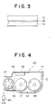
- the image forming apparatus 100 comprises: the drum-like photoreceptor 1 (which will be called a photoreceptor, hereinafter); a scorotron charger 2 which gives a uniform charge on the photoreceptor 1; an optical scanning system 3; developing units 4A, 4B, 4C, 4D in which toners of yellow, magenta, cyan and black are loaded; a pre-transfer charger 61; a scorotron transfer unit 62; a separator 63; a fixing roller 64; a cleaning unit 70; and a discharger 74.
- the photoreceptor 1 comprises a conductive support 1A, a middle layer 1B and a photosensitive layer 1C.
- the thickness of the photosensitive layer 1C is 5 - 100 ⁇ , and preferably 10 - 100 ⁇ .
- the photosensitive layer 1C is composed in such a manner that: the drum-like conductive support 1A made from aluminum is utilized, the diameter of which is 150mm; the intermediate layer 1B made from ethylene-vinyl acetate copolymer, the thickness of which is 0.1 ⁇ m, is formed on the aforementioned support 1A; and the photoconductive layer 1C, the layer thickness of which is 35 ⁇ m, is formed on the aforementioned intermediate layer 1B.
- a drum made of aluminum, steel, copper or the like, the diameter of which is 150mm, is used as the conductive support 1A.
- the following may be used as the conductive support 1A: a belt-like support made of paper or plastic on which a metal layer is laminated or vapor-deposited; or a metallic belt such as a nickel belt made by the method of electroforming.
- the intermediate layer 1B is preferably provided with the following properties: the intermediate layer 1B can withstand a high potential of ⁇ 500 - ⁇ 2000V, for example, in the case of positive charging, the migration of electrons from the conductive support 1C is prevented; and the intermediate layer 1B has a hole mobility so that an excellent light decay characteristic can be obtained due to an avalanche phenomenon. Therefore, a positive charging type of electric charge conveyance material, which is described in the specification of Japanese Patent Application Open to Public Inspection 44662/1988 proposed by the applicant, is preferably added into the intermediate layer 1B by not more than 10 weight %.
- the following resins which are applied to a photosensitive layer for use in electrophotography, may be used for the intermediate layer 1B.
- the photosensitive layer 1C is formed in such a manner that: electric conveyance material is not essentially contained in the photosensitive layer 1C; phthalocyanine particulates, the diameter of which is 0.1-1 ⁇ m, composed of photoconductive pigment, an antioxidant, and a binder resin are mixed and dispersed in a solvent of binder resin, so that a coating slurry can be prepared; the aforementioned coating slurry is coated on the intermediate layer; the coated intermediate layer is dried; and heat treatment is conducted, if necessary.
- a photoconductive material including a photoconductive pigment and an electric charge conveyance material, the weight of which is not more than 1/5, preferably 1/100 - 1/10 of the aforementioned photoconductive pigment, and an antioxidant are dispersed in a binder resin so that a photosensitive layer is formed.
- color toner images are superimposed as registered each other on the photoreceptor, so that a photoreceptor, the spectral sensitivity of which is on the long wavelength side, is needed so that the infrared beam sent from the optical scanning system 3 can be accepted through the color toner images.
- An electrostatic latent image is formed by the optical scanning system 3 in such a manner that a beam optically modulated according to an image density signal of a predetermined number of bits is projected on the circumferential surface of the photoreceptor 1 which has been uniformly charged.
- the optical scanning system 3 comprises: a semiconductor laser 31; collimator lens 32; a polygonal mirror 36; an f ⁇ lens 38; a tilting correction lens 37 to correct the tilt caused by the polygonal mirror 36; and an index sensor 39.
- the index sensor 39 is used as follows: the index sensor 39 detects the surface position of the polygonal mirror 36 which is rotated at a predetermined speed; and optical scanning is conducted according to the modulated image data, which will be described later, while the optical scanning is synchronized with the primary scanning.
- GaAlAs is used for the semiconductor laser 31, and color images are superimposed as registered each other on the photoreceptor 1 in sequence. Accordingly, it is desirable to conduct exposure using light having a wavelength which is less absorbed by each color toner. In this case, the wavelength of the beam is 800nm.
- the developing units 4A, 4B, 4C, 4D have the same structure, wherein the colors of developers to be loaded are different.
- the structure of developing device 40 is explained as follows.
- the developing device 40 is provided with: a sleeve 43 including a magnetic roller 44 having N and S poles which is rotated inside a developing tank made of a lower casing 42 and an upper casing 41; a scraper 45 made of an elastic plate, which is mounted on a stationary member 46 fixed to an upper casing 41, and which comes into contact with a sleeve 43 with pressure; the first and second screw-shaped stirring members 47, 48; and a sleeve cleaning roller 49.
- the first stirring member 47 conveys the developer toward the viewer's side
- the second stirring member 48 conveys the developer to the far side with regard to the viewer.
- a wall 42 is installed between the stirring members 47, 48 so that the developer can not be accumulated in the tank.
- a thin layer forming means composed of a magnetic plate or a magnetic rod may be installed.
- the sleeve cleaning roller 49 is rotated in the direction of an arrow so that the developer which has passed through the developing region and in which the toner component has been consumed, can be scraped off from the sleeve 43. Therefore, the developer conveyed into the developing region can be replaced with a new one, so that the developing conditions are stabilized.
- the sleeve 43 is connected with a development bias circuit 80 which impresses a voltage having a DC current bias component, through a protective resistance (not illustrated in the drawing).
- a two-component type of developer D which is characterized in that: the particle size of the toner is 1-20 ⁇ m; and silica particulates processed by amine compounds or silica particulates to which other additives are added, are used as the electric charge controlling agent.
- Small sized carrier particles are advantageous from the viewpoint of resolving power and gradation reproducibility. For example, when a small carrier, the particle size of which is 5-50 ⁇ m, is used, a uniform height of magnetic brush can be formed on the sleeve 43.
- the development bias circuit 80 is provided with: an AC current power source which supplies an AC bias in order to oscillate the toner between the sleeve 43 and the photoreceptor 1 in the developing region wherein the toner conveyed by the sleeve is electrostatically transferred onto the photoreceptor 1; and a high voltage DC current power source which supplies a DC current bias.
- V DC 800V
- V AC 700V
- the frequency is 3KHz.
- the development bias circuit 80 generates an oscillating electric field between the sleeve 43 and the photoreceptor 1, so that the particles of the developer are oscillated in the space between the sleeve 43 and the photoreceptor 1. Accordingly, a toner image can be formed on the photoreceptor 1 under the condition that developer D does not come into contact with the photoreceptor, so that the toner image formed previously is not damaged.
- a one component type of developer can be also used as developer D in this embodiment.
- the developer does not come into contact with a latent image, so that it is difficult to develop a minute latent image.
- a high ⁇ type of photoreceptor is used so as to form a sharp latent image, development of minute portions can be improved.
- the effect of the present invention in which the high ⁇ photoreceptor is utilized can be increased not only in the case of contact development but also in the case of non-contact development.
- composition of the developer used in the embodiment will be described as follows.
- Materials having the above-described composition are mixed, kneaded and ground. Then, the materials are classified so that the toner, the averaged particle size of which is 3 ⁇ m (by weighing method) , can be obtained. Silica particle was used as an outer additive of the toner. The electric charge of the toner is 20 ⁇ c/g.
- the coloring agent can have the spectral characteristics to prevent the above-described decrease.
- Benzidine Yellow G (C.I.21090), Benzidine Yellow GR (C.I.21100), Permanent Yellow DHG (product of Hoechst Co.), Brilliant Carmine 6B (C.I.15850), Rhodamine 6G Lake (C.I.45160), Rhodamine B Lake (C.I.45170), Phthalocyanine Blue Non Crystal (C.I.74160), Phthalocyanine Green (C.I.74260), Carbon Black, Fat Yellow 5G, Fat Yellow 3G, Fat Red G, Fat Red HRR, Fat Red 5B, Fat Black HB, Zapon Fast Black RE, Zapon Fast Black B, Zapon Fast Blue HFL, Zapon Fast Red BB, Zapon Fast Red GE, Zapon Fast Yellow G, and Quinacridone Red (C.I.465000)
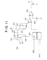
- Fig. 5 is a block diagram showing the first drive circuit of the optical scanning system.
- a drive circuit 300 of an optical scanning system 3 forms an intensity-modulated signal according to an image density signal (image density data) sent from a computer or a scanner, and a semiconductor laser 31 is driven by the aforementioned modulation signal.
- the laser drive circuit 300 may be provided with a means to feed back a signal corresponding to the amount of light of the beam sent from the semiconductor laser 31, and the drive circuit 300 may be driven so that the amount of light can be constant.
- the drive circuit 300 comprises: a reference wave generating circuit 310; a buffer circuit 320; differential amplitude circuits 340, 350; a variable DC power source 360; and a D/A converter 330.
- the reference wave signal generating circuit 310 triangular waves are generated by an integrator which is composed of a variable resistor 311 and a condenser 312.
- the aforementioned triangular wave is inputted into a base terminal of a transistor 321 through a condenser 313 and a protective resistance 315.
- the reference wave signal generating circuit 310 is provided with two variable resistors.
- the variable resistor 311 is provided for adjusting the amplitude of the triangular wave.
- a variable resistor 314 is provided for adjusting the bias or the offset of the triangular wave.
- the triangular wave is inputted into a positive input terminal of a differential amplifier 340 through the buffer circuit 320.
- the differential amplifier 340 differentially amplifies a reference wave which has passed through the buffer circuit 320, and an analog density signal which has been obtained by D/A-converting of a digital image density signal of a predetermined number of bits, for example, 8 bits, by the D/A converter 330. Then, the obtained intensity modulation signal is outputted into the input terminal of the differential amplifier 350.
- the intensity modulation signal inputted into the positive terminal is level-shifted and outputted from the differential amplifier 350.
- This level-shifting corresponds to the white background in the image.
- an intensity modulation signal synchronized with pixel-clock DCK is outputted from the differential amplifier 350. This signal is used as a drive signal to turn on and off the semiconductor laser 31.
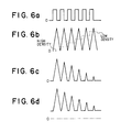
- Fig. 6 is a time chart showing the wave-form of each portion of the first drive circuit.
- the numeral 6a is reference pulse SCK for a reference wave, and pulse SCK is synchronized with pixel clock DCK.
- the signal in 6b shown by a broken line is an analog density signal which has been D/A converted after color correction or gray level correction, and the signal shown by a solid line is a reference wave signal which is an output signal from the buffer 320.
- the numeral 6c is a modulation signal which has been intensity-modulated by the differential amplifier 340. The density signal corresponding to a recorded pixel and the reference signal are synchronized with each other, and an intensity modulation signal corresponding to the image density is generated.
- the numeral 6d is a signal obtained by level-shifting of the intensity-modulation signal. This level-shifting is conducted in accordance with the white background in the image as described above.
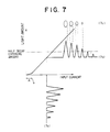
- Fig. 7 is a schematic illustration which explains the relation between the intensity modulation signal which has been level-shifted from the drive circuit in the first embodiment, and the amount of light emitted from a semiconductor laser.
- the graph shows an input and output characteristic showing the relation between the current inputted into the semiconductor laser 31 and the amount of emitted light.
- A represents a region from which light is spontaneously emitted
- ⁇ represents a threshold value.
- inductive emission occurs. In other words, it is a region in which inductive emission is conducted.
- the numeral 7a shows a current to be inputted into the semiconductor laser 31.
- a current which has been level-shifted in accordance with the white background in the image is inputted into the semiconductor laser. In the way described above, the rising time of the semiconductor laser 31 can be improved.
- the numeral 7b shows the amount of light emitted from the semiconductor laser 31 in accordance with an inputted current.
- a one-dotted chain line shows the amount of light needed to half-decay-exposure in the high ⁇ photoreceptor used in this embodiment.
- the photoreceptor is a high ⁇ type, a latent image is not formed when the amount of exposure sent from the semiconductor laser 31 is lower than the amount of half decay exposure, in other words, when the amount of exposure sent from the semiconductor laser 31 is lower than the amount which is necessary to change potential V 0 to 1/2V 0 . Therefore, even when the level-shifted DC current is higher than the threshold value current ⁇ , it can correspond to the white background.
- the semiconductor laser is oscillated even in the portion corresponding to the white background.
- the numeral 7c shows an exposure dot distribution which is recorded on the photoreceptor 1.
- the position of the amount of light to cause the half-decay-exposure is indicated by a broken line.
- a latent image is formed by the photosensitive characteristic of the high ⁇ photoreceptor.
- a latent image composed of various sizes of dots can be obtained according to the density signal, and is shown in the image density distribution of dots obtained by developing the aforementioned latent image. Sharper and smaller dot-shaped latent images can be formed.
- the distribution of exposure of a dot extends wider than the blur portion of the optical scanning system 3. Consequently, there is a tendency that the diameter of a recorded dot in a high density portion is large, and the diameter of a recorded dot in a low density portion is small.
- the image forming process by the image forming apparatus 100 of the embodiment will be explained as follows.
- image exposure is conducted by the beams sent from an optical scanning system 3 so that an electrostatic latent image corresponding to each color is formed on the drum-like photoreceptor 1.
- the electrostatic latent image corresponding to yellow is formed by irradiating the photoreceptor 1 with a laser beam which has been optically modulated by yellow data (digital density data).
- the aforementioned electrostatic latent image corresponding to yellow is developed by the first developing unit 4A, and the first dot-like toner image (a yellow toner image), which is very sharp, is formed on the photoreceptor 1. This first toner image is not transferred onto recording paper.
- the surface potential of the first toner image is discharged by an AC current corona discharge conducted by a discharger, then the first toner image is optically discharged by infrared rays 14. Next, the photoreceptor 1 is charged again by the scorotron charger 2.
- the laser beams are optically modulated by magenta data (digital density data), and the photoreceptor 1 is illuminated by the modulated laser beams so that an electrostatic latent image can be formed.
- This electrostatic latent image is developed by the second developing unit 4b and the second toner image (a magenta toner image) is formed.
- the toner images are developed by the third developing unit 4C in order that the third toner image (a cyan toner image) is formed. In this way, a three-color toner image in which toner images are superimposed, is formed on the photoreceptor 1.
- the fourth toner image (a black toner image) is formed so that a four-color toner image is formed on the photoreceptor 1.
- the photoreceptor has an excellent high ⁇ characteristic. Due to the high ⁇ characteristic, a latent image can be stably formed when the processes of charging and exposure are repeated a plurality of times so that toner images can be superimposed. In other words, even when a toner image is exposed by a laser beam according to a digital signal, a sharp dot-shaped electrostatic latent image in which a fringe is eliminated, can be formed. As a result, a highly sharp toner image can be obtained.
- this four-color toner image is transferred by a transfer unit 62 onto recording paper.
- Recording paper which conveys a transferred toner image is separated from the photoreceptor 1 by a separation electric pole 63, conveyed by a guide and a conveyance belt into a fixing unit 64, fixed by the method of heat fixing, and discharged onto a delivery tray.
- the photoreceptor 1 which has finished transferring of the toner image is prepared for the next multi-color image forming in such a manner that: the residual toner on the surface is removed by a blade, a fur brush or a magnetic brush of a cleaning unit 70 which has been released during toner image forming; and the photoreceptor is discharged by a discharger 74 composed of a corona discharger and a lamp.
- the lamp and the corona discharger 74 may be provided upstream of the cleaning means.
- the discharging process for each toner image forming may be omitted when the DC component in the current inputted into the semiconductor laser 31 is not more than the threshold current ⁇ .
- a sharp image having a high gradation was obtained when the following reference wave was selected: the reference wave was composed of large and small triangular waves, the period of which was twice as long as that of the recording pixel.
- a sharp image having a high resolution was obtained when the same triangular wave was used (the period of which was twice as long as that of the recording pixel).
- image reproduction by a high ⁇ photoreceptor tends to become high contrast, so that it is effective for the reference wave to have a plurality of peaks in one period as described above in order to improve the gradation property.
- a sharp image having a high resolution was obtained when a reference wave composed of the same triangular wave was adopted (one period of which becomes the same as that of the recording pixel).
- a reference wave the period of which is longer than that of a recording pixel, may be adopted.
- the period of which is 4 times as long as that of a recording pixel a desirable result can be obtained.
- intensity modulation in which the semiconductor laser 31 is utilized has been explained.
- the present invention is not limited to this specific embodiment.
- optical modulation can be conducted by a density signal which has been intensity-modulated in the same manner, so that the same effect can be provided.
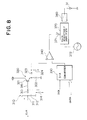
- Fig. 8 is a block diagram showing a drive circuit of the optical scanning system 3 of the second embodiment.
- a drive circuit functions as follows: an analog image density signal is intensity-modulated by a reference signal; a conveyance wave signal is modulated by the intensity-modulation signal; and the aforementioned signal is level-shifted, and the obtained modulation signal is impressed upon the semiconductor laser 31.
- the drive circuit is composed of, a reference wave signal generating circuit 310, a buffer circuit 320, a differential amplifier 340, a D/A converter 330, a variable resistor 371, a variable gain amplifier 370, a high band power amplifier 380, and a conveyance wave signal generating circuit 372.
- a triangular wave is generated by an integrator composed of a variable resistor 311 and a condenser 312. Further, the triangular wave is inputted into a base terminal of a transistor 321 through a condenser 313 and a protective resistor 315.
- the reference wave generating circuit 310 is provided with two variable resistors.
- the variable resistor 311 is provided for adjusting the amplitude of the triangular wave.
- a variable resistor 314 is provided for adjusting the bias and offset of the triangular wave.
- the triangular wave (which is shown by a solid line in 9b in Fig. 9) is outputted into the pisitive input terminal of the differential amplifying circuit 340 through the buffer circuit 320.
- the differential amplifier 340 intensity-modulates the analog image density signal with the reference signal, and inputs the modulation signal into the variable gain amplifier 370 through the variable resistor element 371.
- a conveyance wave, the frequency of which is not less than 600MHz, is amplitude-modulated by the variable gain amplifier 370, and a high frequency voltage obtained by amplifying the signal with the high band power amplifier 380 is impressed upon the electric terminal of the semiconductor laser 31.
- the high band amplifier 380 is also provided with the function of level-shifting the modulation signal using a DC component.
- the numerals 9a-9d in Fig. 9 are time charts showing the wave-form of each portion in the drive circuit of this embodiment.
- the numeral 9a is a reference pulse SCK for a reference wave, and pulse SCK is synchronized with pixel clock DCK.
- the signal indicated by a broken line in 9b is an analog density signal which has been D/A-converted after color correction and gradation correction, and the signal indicated by a solid line is a reference signal which is an output signal from the buffer 320.
- the numeral 9c is an intensity-modulation signal which has been intensity-modulated by the differential amplifier 340.
- the density signal corresponding to a recording pixel is synchronized with the reference signal so that an intensity-modulation signal corresponding to the image density can be generated.
- the numeral 9d shows a modulation signal which is obtained by amplitude-modulating of a conveyance wave signal with the intensity-modulation signal. In this case, it is further shown that the modulation signal is further level-shifted with the high band power amplifier.
- Fig. 10 is a schematic illustration which explains the relation of the amount of light emitted from the semiconductor laser according to the intensity-modulation signal which has been level-shifted from the drive circuit of the second embodiment.
- A is a region from which light is emitted spontaneously
- ⁇ is a threshold current value.
- ⁇ is a threshold current value.
- the numeral 10a shows a current which is inputted into the semiconductor laser 31.
- the current which has been level-shifted by the amount corresponding to the white background of the image is inputted into the semiconductor laser. For that reason, the rising time of the semiconductor laser 31 can be improved.
- the numeral 10b shows the amount of light emitted from the semiconductor laser 31 corresponding to the current.
- a one-dotted chain line shows the amount of light to the half decay exposure in the high ⁇ photoreceptor utilized in this embodiment.
- the photoreceptor is a high ⁇ type. Accordingly, in the case where the amount of exposure given by the semiconductor laser 31 is equal to the amount of light necessary for the half decay exposure voltage 1/2V 0 , a latent image is not formed. Therefore, even when the DC component which has been level-shifted, is more than the threshold value ⁇ , the current corresponds to the white background. Namely, in this embodiment, the semiconductor laser 31 is oscillated even in a portion corresponding to the white background.
- the numeral 10c shows an exposure distribution which is recorded on the photoreceptor 1.
- the portion beyond the light amount to the half decay exposure is indicated by a broken line, and the portion above the broken line is formed as a latent image due to the characteristic of a high ⁇ type of photoreceptor.
- a latent image can be obtained which is composed of large and small sizes of dots according to the density signal, and the distribution shows a dot-like image density distribution formed by developing the aforementioned latent image. Further, a sharper and smaller dot-like latent image can be formed.
- the diameter of the exposed dot is extended due to the blur of the optical scanning system, so that there is a tendency that the diameter of the recorded dot becomes large in a high density portion, and the diameter of the recorded dot becomes small in a low density portion.
- the drive circuit comprises the reference wave signal generating circuit 310, the buffer circuit 320, the differential amplifying circuit 350, the variable DC current power source 360, and the D/A converter 330.
- a triangular wave is generated by an integrator composed of a variable resistor 311 and a condenser 312. Further, the triangular wave is inputted into a base terminal of a transistor 321 through a condenser 313 and a protective resistor 315.
- the reference wave generating circuit 310 is provided with two variable resistors.
- the variable resistor 311 is provided for adjusting the amplitude of the triangular wave.
- a variable resistor 314 is provided for adjusting the bias and offset of the triangular wave.
- the triangular wave is inputted into the positive input terminal of a comparator 341 through the buffer circuit 320.
- the comparator 341 a comparison is made between the reference wave which has passed through the buffer circuit 320 as described above,and the analog density signal which has been obtained by D/A-converting of the digital image density signal of a predetermined number of bits, for example 8 bits, through the D/A converter 330.
- the pulse width modulation signal obtained in the aforementioned manner is outputted into the input terminal of the differential amplifier 350.
- the differential amplifier 350 When the output signal sent from the variable DC current power source 360 is impressed upon the negative input terminal of the differential amplifier 350, the differential amplifier 350 outputs the intensity-modulation signal which has been level-shifted after being inputted into the positive terminal, wherein the intensity-modulation signal is the DC component. The amount which has been level-shifted, corresponds to the white background. In the way described above, the differential amplifier 350 outputs a pulse width signal having a DC component synchronized with pixel clock DCK. This signal is used as a drive signal which turns on and off the semiconductor laser 31.
- Fig. 12 is a time chart showing the wave-form of each portion in the third drive circuit.
- the numeral 12a is reference pulse SCK, and the pulse SCK is synchronized with pixel clock DCK.
- a signal shown by a broken line in 12b is an analog density signal which has been D/A-converted after color correction or gradation correction.
- a signal shown by a solid line is a reference signal which is an output signal sent from the buffer 320.
- the numeral 12c is a modulation signal which has been pulse-width-modulated by the comparator 341. The density signal corresponding to a recorded pixel and the reference signal are synchronized, and a pulse-width-modulation signal is generated corresponding to the image density.
- the numeral 12d is a signal obtained by level-shifting of the pulse-width-modulation signal. The amount of level-shifting corresponds to the white background of the image as described above.
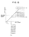
- Fig. 13 is a schematic illustration which explains the relation between a pulse-width-modulation signal which has been level-shifted from the drive circuit of the third embodiment, and the amount of light emitted from the semiconductor laser.
- the graph represents the input and output characteristic which shows the relation between the input current into the semiconductor laser 31 and the amount of emitted light.
- A is a region from which light is emitted spontaneously
- ⁇ is a threshold current value.
- the numeral 13a shows a current which is inputted into the semiconductor laser 31.
- the current which has been level-shifted by the amount corresponding to the white background of the image is inputted into the semiconductor laser. In the way described above, the rising time of the semiconductor 31 can be improved.
- the numeral 13b shows the amount of light emitted from the semiconductor 31 corresponding to the inputted current.
- a one-dotted chain line shows the light amount to the half decay exposure in the high ⁇ photoreceptor utilized in the embodiment.
- the photoreceptor is a high ⁇ type. Accordingly, in the case where the amount of exposure given by the semiconductor laser 31 is equal to the amount of light necessary for the half decay exposure voltage 1/2V 0 , a latent image is not formed. Therefore, even when the DC component which has been level-shifted, is more than the threshold value ⁇ , the current corresponds to the white background. Namely, in this embodiment, the semiconductor laser 31 is oscillated even in a portion corresponding to the white background.
- the numeral 13c shows the distribution of exposure dots which are recorded on the photoreceptor 1.
- the portion equivalent to the half decay exposure is shown by a broken line in the exposure distribution.
- the portion beyond the aforementioned portion is formed into a latent image due to the high ⁇ photoreceptor characteristic. Namely, a latent image can be obtained which is compsed of large and small sizes of dots according to the density signal, and the distribution shows a dot-like image density distribution formed by developing the aforementioned latent image. Accordingly, a sharper and smaller dot-like latent image can be formed.
- the shape of the exposure dot distribution is oval, the distribution of the exposure dot is extended due to the blur of the optical scanning system 3, so that there is a tendency that the diameter of the recorded dot becomes large in a high density portion, and the diameter of the recorded dot becomes small in a low density portion.
- the print density can be changed according to the print content. Namely, when the DC component of the reference wave is shifted, the density can be changed.
- the DC component is larger than the threshold current ⁇ . However, it is possible to set the DC component to a smaller value than the threshold current ⁇ .
- noises become stable with regard to the change of temperature and light feed back and further spike-like noises are not caused.
- the signal shown by a broken line in 14b illustrated in Fig. 14 is an analog density signal which has been D/A-converted after a color correction and gradation correction according to the recording characteristic.
- the signal shown by the broken line is a reference signal which is the output signal sent from the buffer 320 in Fig. 5.
- Vmin corresponds to the minimum (the black background) of the image density signal
- Vmax corresponds to the maximum (the white background) of the image density signal. Since the amplitude of the reference wave exceeds Vmax of the image density signal, exposure is conducted in the white background. A portion of the reference wave amplitude is located below Vmin of the image density signal, so that exposure is partially conducted in the black background. Accordingly, dots can be positively formed in the low density portion, and dots of a small diameter can be formed in the high density portion. In the manner explained above, the recording characteristic of the high ⁇ photoreceptor can be improved.
- the amount of exposure at Vmax corresponding to the white background may be set to a value approximately the same as or smaller than the light amount P 1/2 to the half decay exposure by setting the amplitude of the reference wave signal to a large value instead of the DC component.
- Rasio shows a ratio of the level width (Vmax-Vmin)/2 of the image density signal to the amplitude of the reference wave signal.
- Mark ... shows that the image quality is good
- mark ⁇ shows that the image quality is a little inferior
- mark ' shows that the image quality is a little inferior
- mark ' shows that the image quality is bad.
- the level of amplitude is preferably 1.1-1.5 times that of the level width (Vmax-Vmin) of the image density signal.
- Vmax-Vmin level width of the image density signal.
- the aforementioned embodiment can be applied not only to the drive circuit shown in Fig. 5 but also to other drive circuits.
- Fig. 15 shows the wave-form of each portion in the case when this embodiment is applied to the drive circuit in Fig. 5.
- a solid line shows a case in which an image of high contrast is reproduced
- a a broken line shows a case in which an image of low contrast is reproduced.
- the amplitude is made variable, which is illustrated by Fig. 16 in which the relation between the amplitude of the reference wave and the dot diameter is shown
- the case of small amplitude is shown by a solid line
- the case of large amplitude is shown by a broken line.
- the recording dot diameter becomes small in the more exposed portion (which corresponds to the high density portion)
- the recording dot diameter becomes large in the less exposed portion (which corresponds to the low density portion).
- this embodiment can be applied to other drive circuits.
- the present invention is to provide an image forming apparatus which is characterized in that: an image is formed on a photoreceptor having a light decay characteristic by which the photoreceptor potential is not decayed in the initial period of exposure and sharply decayed in the middle period of exposure, by oscillating a semiconductor laser beam in accordance with a modulation signal obtained by modulating an image density signal with a reference wave signal, wherein a direct current component is included in a modulation signal corresponding to the white background of the aforementioned image density signal. Accordingly, the following effects can be provided to the image forming apparatus of the invention: the response to a drive signal is improved; the variation of beam intensity caused by environmental factors such as heat is decreased; and a latent image can be stably formed.
- an image forming apparatus When the image density signal is pulse-modulated by the reference signal, an image forming apparatus can be provided which can form a sharp and small latent image.
- the image forming apparatus forms an image on a photoreceptor having a light decay characteristic by which the photoreceptor potential is not decayed in the initial period of exposure and is sharply decayed in the middle period of exposure, using a modulation signal which has been obtained by modulating the image density signal by the reference signal.
- a modulation signal which has been obtained by modulating the image density signal by the reference signal.
- the image forming apparatus forms an image on a photoreceptor having a light decay characteristic by which the photoreceptor potential is not decayed in the initial period of exposure and is sharply decayed in the middle period of exposure, using a modulation signal obtained by modulating the image density signal with the reference signal.
- the reference wave signal is made variable, the image forming apparatus can control the image easily and stably.
- the gradation property of an image can be controlled as follows: the diameter of a dot-like toner image, in other words the area of the dot-like toner image, is changed, wherein the dot-like toner image has been obtained by reversal-developing of an electrostatic latent image formed on the high ⁇ type photoreceptor.
- the amount of modulation light is reduced which is necessary to reduce the electrical potential of the high ⁇ type photoreceptor in such a manner that: the high ⁇ type photoreceptor is illuminated with uniform light emitted by an illuminating means before or after or simultaneously with the exposure of modulation light conducted by the optical scanning system on the aforementioned photoreceptor.
- the light decay characteristic of the high ⁇ type photoreceptor is expressed by the portion after dotted line a, so that the photoreceptor accurately responds to the amount of light of the modulated beams sent from the optical scanning system.
- the image forming apparatus of the present invention can adjust the area of the electrostatic latent image which is formed by the modulated light sent from the optical scanning system.
- the gradation of images can be improved by extending the range in which the area of a dot-like toner image can be changed.
- the image forming apparatus of the present invention is characterized in that: illuminating means which can illuminate with a uniform amount of light is provided between the charger and the developing unit along the entire width of the image; and the light amount P 1/2 to the half decay exposure which is necessary to reduce the electrical potential of the high ⁇ type photoreceptor into half, is seemingly reduced so that the photoreceptor can respond to the modulation light sent from the optical scanning system and a sharp electrostatic latent image can be formed.
- An image of high gradation can be formed by reversal-developing of the latent image.
- the aforementioned illuminating means is provided with a variable illumination means by which the amount of illuminating light can be changed, an image of high gradation can be formed without being influenced by environmental factors in the image forming apparatus.
- two kinds of image forming apparatuses provided with different optical scanning systems, are explained as follows.
- the following two kinds of image forming apparatuses have a common structure except the optical scanning system, so that first of all the common structure will be explained.
- Fig. 18 is a perspective view showing the outline of the structure of the image forming apparatus of an embodiment of the present invention.
- a color image forming apparatus 100 of this embodiment conducts shading-correction, gradation correction, masking correction and the like on the image density signal sent from a computer or a scanner after a photoreceptor has been uniformly charged.
- a dot-like electrostatic latent image is formed by a spot exposure which has been intensity-modulated or pulse-width-modulated according to a modulation signal, wherein the modulation signal is obtained by comparing an analog image density signal obtained by D/A-converting the digital image density signal obtained in the manner described above, with a reference signal.
- the obtained dot-like electrostatic latent image is reversal-developed by toner so that a dot-like toner image can be formed.
- the aforementioned exposure and development processes are repeatedly conducted so that a color toner images can be formed on a photoreceptor 1.
- the obtained color toner images are transferred, separated and fixed so that a multicolor image can be obtained.
- the image forming apparatus 100 comprises, a drum-like photoreceptor (which will be called a photoreceptor, hereinafter) which is rotated in the direction of an arrow, a scorotron charger 2 which uniformly gives electric charge on the photoreceptor 1, an optical scanning system 3, developing units 4A, 4B, 4C, 4D which are loaded with toners of yellow, magenta, cyan and black, a pre-transfer charger 61, a scorotron transfer unit 62, a separator 63, a fixing roller 64, a cleaning unit 70, a discharger 14 and illuminating means 80 which uses infrared rays.
- a drum-like photoreceptor which will be called a photoreceptor, hereinafter
- a scorotron charger 2 which uniformly gives electric charge on the photoreceptor 1
- an optical scanning system 3 developing units 4A, 4B, 4C, 4D which are loaded with toners of yellow, magenta, cyan and black
- the illuminating means 80 lights an infrared LED array which has been aligned along the entire print width at intervals corresponding to dot density so that a uniformly charged photoreceptor 1 can be illuminated with infrared rays by one dot line.
- a diffusion plate is provided with the illumination surface of the LED array so that the photoreceptor 1 can be uniformly illuminated.
- the amount of illuminated light emitted by the illumination means 80 is controlled under the amount of light L 1 so that the surface electric potential of the photoreceptor 1 can not be less than V 0 .
- the illuminating means 80 seemingly reduces L 1 and L 2 showing the optical decay characteristic of the photoreceptor 1.
- the light source is not limited to an LED array, and other light sources can be used if the amount of illuminated light can be easily controlled.
- the illuminating means 80 is provided with a light amount regulating means which detects the fluctuation of temperature inside the apparatus and regulates the amount of illumination.
- a variable illumination means is provided which is characterized in that: a surface electrometer (which is not illustrated in the drawing) is provided to the photoreceptor 1 ; and the surface potential caused after illumination by the illumination means 80 and the surface potential caused by optical scanning conducted by the optical scanning system 3 can be detected so that the amount of illumination can be set. In the way described above, a latent image can be formed without being influenced by environmental fluctuations inside the apparatus.
- color toner images are superimposed on the photoreceptor, so that the beams sent from the optical scanning system transmit the color toner images and the electric potential is lowered. Therefore, a photoreceptor, the spectral sensitivity of which is on the long wave side, is necessary. It is preferable that the uniform illuminating light emitted by a uniform illumination means 80 is infrared in the same manner as the writing-in light so that the light can transmit the color toner images. It is preferable that the region illuminated uniformly is limited to an image portion, which is effective to prevent toner from being attracted onto a non-image-forming portion of the photoreceptor due to the lowering of electric potential.
- Fig. 19 is a block diagram showing a drive circuit of the optical scanning system.
- an optical scanning system 3 is composed of collimator 32, a polygonal mirror 36, an f ⁇ lens 38, a tilt correction lens 37a which corrects the tilt caused by the polygonal mirror 36, and an index sensor 39.
- the optical scanning system 3 forms an image on the photoreceptor 1 with an oval beam according to a digital image density of a predetermined bit.
- the index sensor 39 detects the surface position of the polygonal mirror 36 which is rotating at a predetermined speed. The result of the detection is used for optical scanning conducted by modulated image data according to the period of primary scanning.
- a semiconductor laser 31 is made from GaAlAs. Since color toner images are superimposed on the photoreceptor 1 in order, it is preferable to conduct exposure using the light, the wavelength of which is long, so that the absorption of light by color toner can be reduced. In this case, the wavelength of the beam is 800nm.
- a drive circuit 300 of the optical scanning system generates a pulse-width-modulation signal in accordance with an image density signal (image density data) sent from a computer or a scanner, and drives the semiconductor laser 31 with the aforementioned pulse-width-modulation signal.
- the signal corresponding to the amount of beam sent from the semiconductor laser 31, is fed back to the drive circuit, and the drive circuit is driven so that the amount of beam can become constant.
- the drive circuit comprises a reference wave signal generating circuit 310, a buffer circuit 320, a comparator 330, and a D/A-converter 340.
- a triangular wave is generated by an integrator composed of a variable resistor 311 and a condenser 312. Further, the triangular wave is inputted into the buffer circuit 320 through a condenser 313 and a protective resistor 315.
- the reference wave generating circuit 310 is provided with two variable resistors.
- the variable resistor 311 is provided for adjusting the amplitude of the triangular wave.
- a variable resistor 314 is provided for adjusting the bias and offset of the triangular wave.
- the triangular wave is inputted into the plus input terminal of a comparator 330 through the buffer circuit 320.
- the comparator 330 a comparison is made between the reference wave which has passed through the buffer circuit 320 as described above, and the analog density signal which has been obtained by D/A-converting the digital image density signal of a predetermined bit, for example of 8-bit, with the D/A converter 340 so that the data can be a binary digit. Then, the obtained pulse-width-modulation signal is outputted. This signal is used as a drive signal which turns on and off the semiconductor laser 31.
- the numerals 20a-20f in Fig. 20 are time charts which explain the operations of the first optical scanning system and illumination means.
- the numeral 20a shows a pixel clock DCK.
- the numeral 20b is an analog density signal which has been D/A-converted after a color correction or a gradation correction.
- the signal indicated by a chain line shown in the numeral 20c is an analog signal showing the density of a D/A-converted image, and the signal indicated by a solid line is a reference wave signal which is an output signal sent from a differential amplifying circuit 330.
- the numeral 20d is a pulse-width-modulation signal sent from the differential amplifying circuit 330.
- the density signal corresponding to a recording pixel is synchronized with the reference signal, and the pulse-width signal corresponding to the image density signal is generated.
- the numeral 20e shows an exposure dot distribution on the photoreceptor 1.
- the exposure dot distribution is extended due to the blur of the optical scanning system 3.
- the portion indicated by a broken line in the exposure dot distribution, the exposure amount of which is approximately more than the half decay exposure, is formed into a latent image due to the high ⁇ photoreceptor characteristic.
- the amount of light sent from the illumination means 80 is added to the amount of light sent from the optical scanning system 3.
- the light decay characteristic of the photoreceptor 1 seemingly becomes the right portion with regard to a chain line a in the characteristic curve, so that the photoreceptor 1 accurately responds to the amount of an optically modulated beam sent from the optical scanning system.
- the numeral 20f shows an image density distribution of a dot-like image formed by developing a latent image which has been composed of large and small dots in accordance with the density signal.
- a toner image, the gradation property of which has been improved, can be obtained by extending the diameter or the area of the dot-like toner image.
- an illumination means 80 which uniformly illuminates along the entire image width, is provided between the charger 2 and the developing unit 4A, and the illumination means is made to accurately respond to the amount of the optically modulated beam sent from the optical scanning system. In the way described above, an image of high gradation can be formed by reversal development.
- the photosensitivity is defined by an absolute value of electric potential lowering with regard to a minute amount of exposure.
- the amount P of exposure of the illumination means 80 was changed so that image quality could be evaluated, and the following results could be obtained.
- Mark ... shows that the image quality is good
- mark ⁇ shows that the image quality is a little inferior
- mark ' shows that the image quality is bad.
- P 1/2 is the light amount to the half decay exposure necessary to reduce electric potential v 0 of the photoreceptor to 1/2.
- the period of the reference wave can be made longer than the recording pixel synchronization. For example, when the period of the reference wave is 4 times longer than the recording pixel synchronization, a preferable result can be obtained in the same way.
- the pulse width-modulation has been explained in which a semiconductor laser is utilized.
- the present invention is not limited to the specific embodiment.
- optical modulation can be conducted by a density signal which has been pulse-modulated in the same manner, so that the same effect can be provided.
- the image forming process in the image forming apparatus 100 will be explained as follows.
- the photoreceptor is optically discharged by a discharging unit 74 composed of infrared LEDs.
- the amount of light illuminated by the discharging means 14 is preferably more than P 1/2 .
- the amount of discharging light was set to 5 X P 1/2 .
- the photoreceptor 1 is uniformly charged by the scorotron charger 2.
- the image is exposed by the beams sent from the optical scanning system 3, so that an electrostatic latent image corresponding to each color is formed on the drum-like photoreceptor 1.
- An electrostatic latent image corresponding to yellow is formed by the laser beams which have been optically modulated by yellow data (digital density data).
- the aforementioned electrostatic latent image corresponding to yellow is developed by the first developing unit 4A, and the first dot-like toner image (a yellow toner image), which is very sharp, is formed on the photoreceptor 1.
- This first toner image is not transferred onto recording paper, and the photoreceptor 1 is optically discharged by the discharger 14 and charged by the scorotron charger 2 again.
- the laser beams are optically modulated by magenta data (digital density data)
- magenta data digital density data
- the photoreceptor 1 is illuminated with the aforementioned modulated laser beams so that an electrostatic latent image is formed in the photoreceptor 1.
- This electrostatic latent image is developed by the second developing unit 4B and the second toner image (magenta toner image) can be formed.
- the following electrostatic latent image is developed by the third developing unit 4C so that the third toner image (cyan toner) is formed.
- toner images of each color are laminated in sequence so that a three-color-toner image can be formed on the photoreceptor.
- the fourth toner image (a black toner image) is formed so that a four-color toner image in which each color is laminated in order is formed on the photoreceptor 1.
- the photoreceptor is provided with an excellent high ⁇ characteristic. Further, even when charging, exposure and development are conducted on a toner image a plurality of times in order to superimpose toner images, a latent image can be stably formed. In other words, even when a toner image is illuminated with a beam in accordance with a digital signal, a sharp dot-like electrostatic latent image without any fringe can be formed, and as a result, a sharp toner image can be obtained.
- these four-color toner image is transferred onto recording paper supplied by a paper supply unit by the action of the transfer unit 62.
- Recording paper having a transferred toner image is separated from the photoreceptor 1 by the separating electrode 63, conveyed by a guide and a conveyance belt, conveyed into the fixing unit 64 so that the transferred image can be fixed, and delivered onto a delivery paper tray.
- the residual toner on the photoreceptor 1 is removed by a blade, a fur brush, or a magnetic brush in the cleaning unit 70 which has been released during toner image forming.
- the photoreceptor is discharged by a lamp or the corona discharger 74, which has not been used during toner image forming, so that the next multi-color image forming can be prepared.
- the lamp and the discharger 74 may be placed before the cleaning process.
- the electric-potential lowering can be prevented in the non-image region, so that the adhesion of toner can be prevented in the non-image region.
- Fig. 21 is a perspective view showing the second optical scanning system.
- the optical scanning system is operated as follows: the circumferential surface of the photoreceptor 1, which has been uniformly charged, is exposed with a beam which has been optically modulated by an image signal obtained by intensity-modulating a density signal with a reference signal.
- the optical scanning system comprises: a semiconductor laser 131, a beam compressor 132, an acoustic optical modulator (which is called an AOM) 133, a beam expander 134, a cylindrical lens 135, a polygonal mirror 136, a toroidal lens 137, and an F ⁇ lens 138.
- AOM acoustic optical modulator
- An index sensor 139 detects the surface position of the poligonal mirror 136, and the result of the detection is utilized for conducting optical scanning using the modulated image data which will be described later, wherein the period of the primary scanning direction is used in the aforementioned optical scanning.
- a semiconductor laser 31 is made from GaAlAs. Since color toner images are superimposed on the photoreceptor 1 in order, it is preferable to conduct exposure using the light, the wave length of which is long, so that the absorption of light by color toner can be reduced. In this case, the wavelength of the beam is 800nm.
- the beam compressor 132 reduces the diameter of the beam projected into the AMO 33 to 1/3 so that the modulation band can be extended.
- the beam expander 34 expands the beam diameter to its original size.
- the polygonal mirror 136 is an optical deflector, and the cylindrical lens 135 and the toroidal lens 137, which are placed close to the polygonal mirror 136, forms an optical correction system which corrects the tilt of the polygonal mirror 136 so that the unevenness of pitch of the scanning lines caused by the tilt can be decreased.
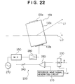
- Fig. 22 is a block diagram showing the drive circuit of the acoustic optical converter of this embodiment.
- AMO 133 is an element which converts an electric signal including an image signal, into an optical signal.
- AMO 133 is composed in such a manner that: electrodes 133a, 133b are provided on both sides of a piezoelectric-crystal element 133c such as heavy flint glass, TiO 2 , and PbMnO 4 .
- a drive circuit 200 comprises a reference wave generating circuit 210, a differential amplifier 220, a D/A converter 230, a variable resistor 240, a variable gain amplifier 250, a high band power amplifier 260, and a conveyance wave generating circuit 270.
- an analog image density signal obtained by D/A-converting a digital image density signal of 8-bit, and a reference signal are modulated by the differential amplifier 220, and the modulated signal is inputted into the variable amplifier 250.
- a conveyance wave is amplitude-modulated by the variable gain amplifier 250, and a high frequency voltage obtained by amplifying the aforementioned signal by the high frequency band power amplifier 260, is impressed upon the electrode 133b.
- AOM functions as follows: a high frequency voltage is impressed upon electrodes so that ultrasonic waves can be generated by a piezoelectric vibrator; the generated ultrasonic waves are transmitted; and a refractive index is changed by the compressional ultrasonic waves due to photo-elasticity of the medium.
- the change of the refractive index made by ultrasonic waves in the manner described above functions as a phase grating with regard to the incident light, and the light which is incident on the ultrasonic wave surface by Bragg angle is diffracted.
- AOM 133 conducts optical modulation by controlling the occurrence of ultrasonic waves in accordance with the image density signal.
- primary light L 1 is used as the modulated light.
- the numerals 23a-23f in Fig. 23 are time charts which explain the image forming process conducted by the second optical scanning means and the illumination means .
- the numeral 23a shows pixel clock DCK to be recorded.
- the numeral 23b is an analog density signal showing the density of an image which has been D/A-converted after the color correction and gradation correction.
- a solid line in 23c is a reference wave signal sent from the reference wave generating circuit 210.
- the time chart 23c shows the relation between the density signal shown in 23b (which is illustrated by a broken line in 23c) and the reference wave signal (which is illustrated by a solid line in 23c) sent from the reference wave signal generating circuit 210.
- the numeral 23d shows an output signal sent from a differential amplifying circuit 220 in Fig.
- the numeral 23d shows a modulation signal obtained by comparing the reference signal with the analog density signal, wherein the amplification is conducted in the manner of differential amplification. This modulation is synchronized with the density signal corresponding to a recording pixel, and the reference signal.
- the numeral 23e shows an exposure distribution on the photoreceptor 1 which is formed by the modulated light which has been modulated by impressing a high frequency voltage, which has been amplitude-modulated by the modulation signal, upon AMO133. In this case, the exposure distribution is the amount of emitted light multiplied by MTF of the optical system. The exposure dot distribution is extended more than the signal shown by 23d due to the blur of the optical system.
- the portion more than the light amount to the half decay exposure which is the amount of exposure necessary for reducing the voltage (V 0 ) of the photoreceptor to 1/2, is formed into a latent image due to the high ⁇ photoreceptor characteristic.
- the amount of light from the optical scanning system 3 is increased by adding of the light uniformly illuminated by the illumination means 80.
- the light decay characteristic of the photoreceptor 1 seemingly becomes the right portion with regard to a chain line a in the characteristic curve, so that the photoreceptor 1 accurately responds to the amount of an optically modulated beam sent from the optical scanning system 130.
- the numeral 23f shows a dot-like image density distribution, wherein the image is obtained by developing a latent image formed by large and small dots in accordance with the density signal. In this way, the range is extended in which the dot-like area of a toner image can be varied.
- gradation and resolving power can be easily selected in accordance with the content of the print.
- adjustment can be performed in accordance with the image by changing the size of a triangular wave continuously.
- the amplitude of the reference wave when the amplitude of the reference wave is changed, the gradation can be varied.
- the density When the DC component of the reference wave is shifted together, the density can be changed.
- the amplitude is changed, for example, the amplitude is made large, an image can be obtained in which gradation property has been improved.
- the amplitude is the same, an image can be obtained in which a resolving power has priority.
- an image forming apparatus in which the high ⁇ photoreceptor 1 is illuminated with an optically modulated beam sent from the optical scanning systems 3, or 130 so that a dot-like electrostatic latent image can be formed and the obtained latent image is reversal-developed, and by which the middle tone can be accurately reproduced by dots.
- intensity modulation is performed by the differential amplifier 330 shown in Fig. 19; and an image is formed according to the time charts shown in Fig. 23.
- optical modulation can be performed by an intensity-modulated image density signal in the same way, and the same effect can be obtained.
- An image forming apparatus 100 can be provided in which the high ⁇ photoreceptor 1 is illuminated with a beam sent from the optical scanning systems 3, 130 conducting optical modulation, so that a dot-like electrostatic latent image is formed, and which is characterized in that: an illuminating means is provided along the entire width of the image so that a uniform amount of light can be illuminated in order to form an image in which a middle tone can be accurately reproduced.
- the amount of illuminating light by the illumination means 80 is variable, so that the photosensitivity of the photoreceptor can be practically changed. Accordingly, the illumination means 80 can be utilized as an image density regulating means.
- An image forming apparatus 100 can be provided in which the amount of illuminating light emitted by the illumination means 80 is changed by a variable illuminating means so that a middle tone can be accurately reproduced by dots without being influenced by the fluctuation of environmental factors.
- a uniform illumination is performed before or after image forming in order to release a trap in the photoreceptor, wherein the illumination is performed as a discharging means.
- an AC current corona discharge is utilized for the purpose described above.
- an optical discharging process by a discharging means 14 is adopted in order to prevent the accumulation of illuminating light emitted from the illumination means 80.
- an image forming apparatus in which the high ⁇ photoreceptor is illuminated with an optically modulated beam sent from the optical scanning system so that a dot-like electrostatic latent image can be formed, and which is characterized in that a uniform illumination is conducted by an illumination means before or after, or simultaneously with the illumination of the aforementioned modulated beam in order to obtain an image in which a middle tone is accurately reproduced.
- the present invention is to provide an image forming apparatus in which a middle tone can be accurately reproduced by utilizing modulated light which has been modulated by intensity-modulation or pulse-width modulation.
- an image forming method can be provided by which a middle tone of an image can be accurately reproduced by dots.
- An image forming apparatus can be provided in which a middle tone can be accurately reproduced by dots when the amount of illuminating light is changed by the aforementioned illumination means.
- the present invention is to provide an image forming apparatus in which a high ⁇ photoreceptor is illuminated with a modulated beam sent from an optical scanning system so that a dot-like electrostatic latent image is formed and the aforementioned latent image is reversal-developed, and which is characterized in that: an illumination means is provided so that a uniform amount of light can be illuminated along the entire image width, so that a middle tone can be accurately reproduced by dots.
- the present invention is to provide an image forming apparatus in which the illuminating region is limited to an image forming region, so that a middle tone can be accurately reproduced by dots.
- the present invention is to provide an image forming apparatus in which the aforementioned illumination means is provided with a variable illumination means, so that a middle tone can be accurately reproduced without being influenced by the fluctuation of environmental factors.
Landscapes
- Engineering & Computer Science (AREA)
- Multimedia (AREA)
- Signal Processing (AREA)
- Physics & Mathematics (AREA)
- Optics & Photonics (AREA)
- Exposure Or Original Feeding In Electrophotography (AREA)
- Laser Beam Printer (AREA)
- Color, Gradation (AREA)
Claims (9)
- Appareil pour la formation électrophotographique d'images, cet appareil incluant un photorécepteur (1) portant une image réalisée en réponse à une exposition lumineuse, ainsi qu'un moyen d'enregistrement d'images pourvu d'un générateur (31) de rayons laser, et comportant également un circuit d'entraînement (300) du générateur assurant le balayage et l'exposition lumineuse de ladite surface d'image au moyen d'un rayon laser en vue de l'enregistrement de ladite image latente sur ladite surface de formation d'images, ledit circuit d'entraînement du générateur (300) étant pourvu d'un générateur de signaux (310) assurant l'émission d'un signal d'ondes de référence, ainsi qu'un comparateur (350) permettant la comparaison du niveau des signaux de densité d'images avec le niveau du signal des ondes de référence et adapté à moduler les signaux de densité d'images sur la base du signal émis des ondes de référence, et à entraîner le générateur de rayons laser (31) conformément aux signaux émis des ondes de référence,caractérisé en ce queledit photorécepteur (1) possède une caractéristique de désintégration lumineuse telle que lorsque la valeur d'exposition lumineuse à un point exposé de la surface de l'image est inférieure à une valeur critique donnée, le potentiel électrique du point exposé se désintègre légèrement, et lorsque la valeur d'exposition lumineuse d'un point exposé de la surface d'image est supérieure à la valeur critique donnée, le potentiel électrique du point exposé se désintègre fortement, et en ce que le générateur de signaux (310) fixe le niveau maximum du signal des ondes de référence de façon telle qu'il sera supérieur au niveau maximum du signal de densité d'image correspondant à une image blanche afin que, lorsque cette image est une image blanche, le générateur de rayons laser (31) émette une valeur initiale de rayons laser comportant une valeur initiale d'exposition lumineuse, ledit générateur de signaux (310) fixant la valeur initiale d'exposition lumineuse de façon telle qu'elle soit inférieure à la valeur critique prédéterminée, afin d'éviter ainsi que la valeur initiale des rayons laser destinés à la formation d'une image blanche ne forme une image latente sur ladite surface d'image.
- Appareil de formation d'images suivant la revendication 1,caractérisé en ce queledit générateur de signaux (310) est adapté à changer l'amplitude du signal des ondes de référence.
- Appareil de formation d'images suivant l'une des revendications 1 ou 2,caractérisé en ce queledit générateur de signaux (310) fixe le niveau minimum du signal des ondes de référence de manière telle qu'il sera inférieur au niveau minimum du signal de densité d'image.
- Appareil de formation d'images suivant l'une des revendications 1 à 3,caractérisé en ce quele générateur de signaux (310) émet le signal des ondes de référence sous forme d'un triangle dont l'apex indique le niveau maximum du signal des ondes de référence et dont la base indique le niveau minimum du signal des ondes de référence.
- Appareil de formation d'images suivant l'une des revendications 1 à 4,caractérisé en ce quele circuit d'entraînement du générateur (300) module la durée d'impulsion du signal de densité d'image.
- Appareil de formation d'images suivant l'une des revendications 1 à 5,caractérisé en ce quele circuit d'entraînement (300) du générateur comprend un circuit (372) d'émission de signaux d'ondes à haute fréquence, et en ce que ledit circuit d'entraînement (300) du générateur module l'amplitude des signaux des ondes à haute fréquence sur la base des signaux modulés de densité d'image et entraîne le générateur (31) de rayons laser conformément aux signaux modulés des ondes à haute fréquence.
- Appareil de formation d'images suivant l'une des revendications 1 à 6,caractérisé en ce queledit appareil comprend des moyens d'exposition lumineuse (80) assurant une exposition lumineuse uniforme de la surface de formation d'images avec une quantité de lumière qui est inférieure à la quantité critique prédéterminée.
- Appareil de formation d'images suivant la revendication 7,caractérisé en ce quele moyen d'exposition lumineuse (80) réalise ladite exposition lumineuse uniforme de façon essentiellement simultanémée au balayage et l'exposition lumineuse de la surface de formation d'images effectués à l'aide du moyen d'enregistrement d'images, ou bien à un moment immédiatement avant le balayage et l'exposition lumineuse de la surface de formation d'images effectués à l'aide du moyen d'enregistrement d'images.
- Appareil de formation d'images suivant l'une des revendications 6 à 9,caractérisé en ce queledit moyen d'exposition réalise ladite exposition lumineuse uniforme sur une partie de formation d'images des surfaces d'image.
Applications Claiming Priority (8)
| Application Number | Priority Date | Filing Date | Title |
|---|---|---|---|
| JP9668590A JPH03293687A (ja) | 1990-04-12 | 1990-04-12 | 画像形成装置 |
| JP96685/90 | 1990-04-12 | ||
| JP11828090A JPH0414073A (ja) | 1990-05-08 | 1990-05-08 | 画像形成方法及びその画像形成装置 |
| JP118280/90 | 1990-05-08 | ||
| JP2139138A JPH0432870A (ja) | 1990-05-29 | 1990-05-29 | 画像形成装置 |
| JP139139/90 | 1990-05-29 | ||
| JP139138/90 | 1990-05-29 | ||
| JP2139139A JPH0432871A (ja) | 1990-05-29 | 1990-05-29 | 画像形成装置 |
Publications (3)
| Publication Number | Publication Date |
|---|---|
| EP0451770A2 EP0451770A2 (fr) | 1991-10-16 |
| EP0451770A3 EP0451770A3 (en) | 1992-08-05 |
| EP0451770B1 true EP0451770B1 (fr) | 1996-06-19 |
Family
ID=27468459
Family Applications (1)
| Application Number | Title | Priority Date | Filing Date |
|---|---|---|---|
| EP91105563A Expired - Lifetime EP0451770B1 (fr) | 1990-04-12 | 1991-04-09 | Appareil de formation d'images |
Country Status (2)
| Country | Link |
|---|---|
| US (1) | US5255014A (fr) |
| EP (1) | EP0451770B1 (fr) |
Families Citing this family (7)
| Publication number | Priority date | Publication date | Assignee | Title |
|---|---|---|---|---|
| DE69107525T2 (de) * | 1990-05-21 | 1995-07-20 | Konishiroku Photo Ind | Bilderzeugungsgerät und -verfahren. |
| US5436644A (en) * | 1991-09-18 | 1995-07-25 | Konica Corporation | Image forming method |
| EP0547495B1 (fr) * | 1991-12-19 | 1997-08-20 | Sharp Kabushiki Kaisha | Appareil de formation d'images |
| JPH06227033A (ja) * | 1993-02-01 | 1994-08-16 | Minolta Camera Co Ltd | デジタル画像形成装置 |
| GB0009134D0 (en) * | 2000-04-13 | 2000-05-31 | Fujifilm Electronic Imaging Li | AOM compensation using PWM |
| JP2004102273A (ja) * | 2002-08-22 | 2004-04-02 | Canon Inc | 画像形成装置 |
| JP2007143111A (ja) * | 2005-10-21 | 2007-06-07 | Canon Inc | 情報処理装置及び情報処理装置の制御方法 |
Family Cites Families (6)
| Publication number | Priority date | Publication date | Assignee | Title |
|---|---|---|---|---|
| JP2647366B2 (ja) * | 1985-08-29 | 1997-08-27 | キヤノン株式会社 | 画像処理装置 |
| JP3004991B2 (ja) * | 1988-04-18 | 2000-01-31 | キヤノン株式会社 | 画像処理装置 |
| EP0624025B1 (fr) * | 1988-09-27 | 1999-09-01 | Canon Kabushiki Kaisha | Dispositif de génération d'images |
| US5025272A (en) * | 1988-12-28 | 1991-06-18 | Konica Corporation | Dot exposure type image forming apparatus |
| JPH02282277A (ja) * | 1988-12-28 | 1990-11-19 | Konica Corp | 画像形成装置 |
| US5017944A (en) * | 1989-03-06 | 1991-05-21 | Victor Company Of Japan, Ltd. | Control system for information recording laser beam |
-
1991
- 1991-04-09 US US07/682,732 patent/US5255014A/en not_active Expired - Fee Related
- 1991-04-09 EP EP91105563A patent/EP0451770B1/fr not_active Expired - Lifetime
Also Published As
| Publication number | Publication date |
|---|---|
| EP0451770A3 (en) | 1992-08-05 |
| US5255014A (en) | 1993-10-19 |
| EP0451770A2 (fr) | 1991-10-16 |
Similar Documents
| Publication | Publication Date | Title |
|---|---|---|
| EP1548514B1 (fr) | Appareil de formation d'image et procédé de formation d'image | |
| JPS63144655A (ja) | 画像形成装置の画質制御方法 | |
| US5172132A (en) | Digital image forming device and method for forming an image from a plurality of dots | |
| EP0451770B1 (fr) | Appareil de formation d'images | |
| US5357317A (en) | Electrostatic recording apparatus using variable bias developing voltage | |
| US7715741B2 (en) | Image forming apparatus with a toner image density feature and related method | |
| EP0464349B1 (fr) | Appareil et procédé de formation d'image | |
| JPH0293667A (ja) | 画像形成装置 | |
| EP0465074A1 (fr) | Appareil pour former des images | |
| JP3155817B2 (ja) | 画像形成装置 | |
| JP2963727B2 (ja) | 4元数を用いた連続ハーフトーン再現方法 | |
| US5783343A (en) | Image forming method and apparatus using pretransfer erase | |
| JP3125192B2 (ja) | 画像形成方法 | |
| JP2000293068A (ja) | 画像形成装置 | |
| JP5089183B2 (ja) | 画像形成装置 | |
| JPH0414073A (ja) | 画像形成方法及びその画像形成装置 | |
| JPH04251875A (ja) | 画像形成装置 | |
| JP2983320B2 (ja) | 画像形成装置 | |
| JP3466791B2 (ja) | 画像形成装置 | |
| JPH03255480A (ja) | ディジタル画像形成装置 | |
| JPH0627778A (ja) | 画像形成装置 | |
| JP3110953B2 (ja) | 画像形成装置 | |
| JP2002361922A (ja) | 画像形成装置 | |
| JPH05127498A (ja) | 画像形成装置 | |
| JPH0432871A (ja) | 画像形成装置 |
Legal Events
| Date | Code | Title | Description |
|---|---|---|---|
| PUAI | Public reference made under article 153(3) epc to a published international application that has entered the european phase |
Free format text: ORIGINAL CODE: 0009012 |
|
| AK | Designated contracting states |
Kind code of ref document: A2 Designated state(s): DE GB IT NL |
|
| PUAL | Search report despatched |
Free format text: ORIGINAL CODE: 0009013 |
|
| AK | Designated contracting states |
Kind code of ref document: A3 Designated state(s): DE GB IT NL |
|
| 17P | Request for examination filed |
Effective date: 19930107 |
|
| 17Q | First examination report despatched |
Effective date: 19941103 |
|
| GRAH | Despatch of communication of intention to grant a patent |
Free format text: ORIGINAL CODE: EPIDOS IGRA |
|
| RBV | Designated contracting states (corrected) |
Designated state(s): GB |
|
| REG | Reference to a national code |
Ref country code: DE Ref legal event code: 8566 |
|
| GRAA | (expected) grant |
Free format text: ORIGINAL CODE: 0009210 |
|
| AK | Designated contracting states |
Kind code of ref document: B1 Designated state(s): GB |
|
| PLBE | No opposition filed within time limit |
Free format text: ORIGINAL CODE: 0009261 |
|
| STAA | Information on the status of an ep patent application or granted ep patent |
Free format text: STATUS: NO OPPOSITION FILED WITHIN TIME LIMIT |
|
| 26N | No opposition filed | ||
| PGFP | Annual fee paid to national office [announced via postgrant information from national office to epo] |
Ref country code: GB Payment date: 20010404 Year of fee payment: 11 |
|
| REG | Reference to a national code |
Ref country code: GB Ref legal event code: IF02 |
|
| PG25 | Lapsed in a contracting state [announced via postgrant information from national office to epo] |
Ref country code: GB Free format text: LAPSE BECAUSE OF NON-PAYMENT OF DUE FEES Effective date: 20020409 |
|
| GBPC | Gb: european patent ceased through non-payment of renewal fee |
Effective date: 20020409 |