EP0450862A2 - Dünnes organisches Filmelement - Google Patents
Dünnes organisches Filmelement Download PDFInfo
- Publication number
- EP0450862A2 EP0450862A2 EP91302714A EP91302714A EP0450862A2 EP 0450862 A2 EP0450862 A2 EP 0450862A2 EP 91302714 A EP91302714 A EP 91302714A EP 91302714 A EP91302714 A EP 91302714A EP 0450862 A2 EP0450862 A2 EP 0450862A2
- Authority
- EP
- European Patent Office
- Prior art keywords
- film
- substrate
- organic thin
- thin film
- layer
- Prior art date
- Legal status (The legal status is an assumption and is not a legal conclusion. Google has not performed a legal analysis and makes no representation as to the accuracy of the status listed.)
- Granted
Links
- 239000010409 thin film Substances 0.000 title claims abstract description 119
- 239000000758 substrate Substances 0.000 claims abstract description 210
- OKTJSMMVPCPJKN-UHFFFAOYSA-N Carbon Chemical compound [C] OKTJSMMVPCPJKN-UHFFFAOYSA-N 0.000 claims abstract description 49
- 229910052799 carbon Inorganic materials 0.000 claims abstract description 20
- 239000000126 substance Substances 0.000 claims abstract description 7
- 238000000034 method Methods 0.000 claims description 88
- 238000001771 vacuum deposition Methods 0.000 claims description 41
- 238000012546 transfer Methods 0.000 claims description 18
- 239000004215 Carbon black (E152) Substances 0.000 claims description 6
- 229930195733 hydrocarbon Natural products 0.000 claims description 6
- 150000002430 hydrocarbons Chemical class 0.000 claims description 6
- 238000006116 polymerization reaction Methods 0.000 claims description 5
- 238000001179 sorption measurement Methods 0.000 claims description 3
- 239000010410 layer Substances 0.000 abstract description 149
- 230000005684 electric field Effects 0.000 abstract description 23
- 230000007704 transition Effects 0.000 abstract description 10
- 230000000694 effects Effects 0.000 abstract description 3
- 239000002344 surface layer Substances 0.000 abstract description 3
- 239000010408 film Substances 0.000 description 321
- VYPSYNLAJGMNEJ-UHFFFAOYSA-N silicon dioxide Inorganic materials O=[Si]=O VYPSYNLAJGMNEJ-UHFFFAOYSA-N 0.000 description 40
- 235000012239 silicon dioxide Nutrition 0.000 description 26
- 239000013078 crystal Substances 0.000 description 18
- JAIHDOVRCZNXDU-UHFFFAOYSA-N violanthrene Chemical compound C12=C3C4=CC=C2C2=CC=CC=C2CC1=CC=C3C1=CC=C2CC3=CC=CC=C3C3=CC=C4C1=C32 JAIHDOVRCZNXDU-UHFFFAOYSA-N 0.000 description 18
- 238000002441 X-ray diffraction Methods 0.000 description 17
- 125000003118 aryl group Chemical group 0.000 description 15
- VPUGDVKSAQVFFS-UHFFFAOYSA-N coronene Chemical compound C1=C(C2=C34)C=CC3=CC=C(C=C3)C4=C4C3=CC=C(C=C3)C4=C2C3=C1 VPUGDVKSAQVFFS-UHFFFAOYSA-N 0.000 description 14
- 238000004519 manufacturing process Methods 0.000 description 14
- 239000010453 quartz Substances 0.000 description 14
- 229910052681 coesite Inorganic materials 0.000 description 13
- 229910052906 cristobalite Inorganic materials 0.000 description 13
- 229920000205 poly(isobutyl methacrylate) Polymers 0.000 description 13
- 239000000377 silicon dioxide Substances 0.000 description 13
- 229910052682 stishovite Inorganic materials 0.000 description 13
- 229910052905 tridymite Inorganic materials 0.000 description 13
- 229910002804 graphite Inorganic materials 0.000 description 12
- 239000010439 graphite Substances 0.000 description 12
- CLYVDMAATCIVBF-UHFFFAOYSA-N pigment red 224 Chemical compound C=12C3=CC=C(C(OC4=O)=O)C2=C4C=CC=1C1=CC=C2C(=O)OC(=O)C4=CC=C3C1=C42 CLYVDMAATCIVBF-UHFFFAOYSA-N 0.000 description 12
- PCCVSPMFGIFTHU-UHFFFAOYSA-N tetracyanoquinodimethane Chemical compound N#CC(C#N)=C1C=CC(=C(C#N)C#N)C=C1 PCCVSPMFGIFTHU-UHFFFAOYSA-N 0.000 description 11
- 238000000151 deposition Methods 0.000 description 10
- YXFVVABEGXRONW-UHFFFAOYSA-N Toluene Chemical compound CC1=CC=CC=C1 YXFVVABEGXRONW-UHFFFAOYSA-N 0.000 description 9
- MWPLVEDNUUSJAV-UHFFFAOYSA-N anthracene Chemical compound C1=CC=CC2=CC3=CC=CC=C3C=C21 MWPLVEDNUUSJAV-UHFFFAOYSA-N 0.000 description 9
- 230000008021 deposition Effects 0.000 description 8
- 230000003287 optical effect Effects 0.000 description 8
- 239000012808 vapor phase Substances 0.000 description 8
- 238000004381 surface treatment Methods 0.000 description 7
- XKRFYHLGVUSROY-UHFFFAOYSA-N Argon Chemical compound [Ar] XKRFYHLGVUSROY-UHFFFAOYSA-N 0.000 description 6
- 230000001133 acceleration Effects 0.000 description 6
- -1 anthantholene Chemical compound 0.000 description 6
- 230000008859 change Effects 0.000 description 6
- 238000006482 condensation reaction Methods 0.000 description 6
- 230000007935 neutral effect Effects 0.000 description 6
- RZJRJXONCZWCBN-UHFFFAOYSA-N octadecane Chemical compound CCCCCCCCCCCCCCCCCC RZJRJXONCZWCBN-UHFFFAOYSA-N 0.000 description 6
- XLYOFNOQVPJJNP-UHFFFAOYSA-N water Substances O XLYOFNOQVPJJNP-UHFFFAOYSA-N 0.000 description 6
- 150000001875 compounds Chemical class 0.000 description 5
- 238000010894 electron beam technology Methods 0.000 description 5
- 229910052751 metal Inorganic materials 0.000 description 5
- 239000002184 metal Substances 0.000 description 5
- 239000002245 particle Substances 0.000 description 5
- IEQIEDJGQAUEQZ-UHFFFAOYSA-N phthalocyanine Chemical compound N1C(N=C2C3=CC=CC=C3C(N=C3C4=CC=CC=C4C(=N4)N3)=N2)=C(C=CC=C2)C2=C1N=C1C2=CC=CC=C2C4=N1 IEQIEDJGQAUEQZ-UHFFFAOYSA-N 0.000 description 5
- 239000000243 solution Substances 0.000 description 5
- VGGSQFUCUMXWEO-UHFFFAOYSA-N Ethene Chemical compound C=C VGGSQFUCUMXWEO-UHFFFAOYSA-N 0.000 description 4
- 239000005977 Ethylene Substances 0.000 description 4
- 229910002370 SrTiO3 Inorganic materials 0.000 description 4
- 239000012300 argon atmosphere Substances 0.000 description 4
- 230000015572 biosynthetic process Effects 0.000 description 4
- GVEPBJHOBDJJJI-UHFFFAOYSA-N fluoranthrene Natural products C1=CC(C2=CC=CC=C22)=C3C2=CC=CC3=C1 GVEPBJHOBDJJJI-UHFFFAOYSA-N 0.000 description 4
- 239000007789 gas Substances 0.000 description 4
- FFUAGWLWBBFQJT-UHFFFAOYSA-N hexamethyldisilazane Chemical compound C[Si](C)(C)N[Si](C)(C)C FFUAGWLWBBFQJT-UHFFFAOYSA-N 0.000 description 4
- 230000003993 interaction Effects 0.000 description 4
- 238000010884 ion-beam technique Methods 0.000 description 4
- 239000000463 material Substances 0.000 description 4
- BBEAQIROQSPTKN-UHFFFAOYSA-N pyrene Chemical compound C1=CC=C2C=CC3=CC=CC4=CC=C1C2=C43 BBEAQIROQSPTKN-UHFFFAOYSA-N 0.000 description 4
- 239000002904 solvent Substances 0.000 description 4
- UGNWTBMOAKPKBL-UHFFFAOYSA-N tetrachloro-1,4-benzoquinone Chemical compound ClC1=C(Cl)C(=O)C(Cl)=C(Cl)C1=O UGNWTBMOAKPKBL-UHFFFAOYSA-N 0.000 description 4
- FHCPAXDKURNIOZ-UHFFFAOYSA-N tetrathiafulvalene Chemical compound S1C=CSC1=C1SC=CS1 FHCPAXDKURNIOZ-UHFFFAOYSA-N 0.000 description 4
- 229910052723 transition metal Inorganic materials 0.000 description 4
- 150000003624 transition metals Chemical class 0.000 description 4
- NNQWYGKROBKYQC-UHFFFAOYSA-N 2,9,16,23-tetra-tert-butyl-29h,31h-phthalocyanine Chemical compound C12=CC(C(C)(C)C)=CC=C2C(N=C2NC(C3=CC=C(C=C32)C(C)(C)C)=N2)=NC1=NC([C]1C=CC(=CC1=1)C(C)(C)C)=NC=1N=C1[C]3C=CC(C(C)(C)C)=CC3=C2N1 NNQWYGKROBKYQC-UHFFFAOYSA-N 0.000 description 3
- 229910052786 argon Inorganic materials 0.000 description 3
- 238000011156 evaluation Methods 0.000 description 3
- 230000002209 hydrophobic effect Effects 0.000 description 3
- 238000002156 mixing Methods 0.000 description 3
- 229940038384 octadecane Drugs 0.000 description 3
- 125000002080 perylenyl group Chemical group C1(=CC=C2C=CC=C3C4=CC=CC5=CC=CC(C1=C23)=C45)* 0.000 description 3
- CSHWQDPOILHKBI-UHFFFAOYSA-N peryrene Natural products C1=CC(C2=CC=CC=3C2=C2C=CC=3)=C3C2=CC=CC3=C1 CSHWQDPOILHKBI-UHFFFAOYSA-N 0.000 description 3
- 238000006068 polycondensation reaction Methods 0.000 description 3
- 229920000642 polymer Polymers 0.000 description 3
- 238000011160 research Methods 0.000 description 3
- 239000004065 semiconductor Substances 0.000 description 3
- PPDADIYYMSXQJK-UHFFFAOYSA-N trichlorosilicon Chemical class Cl[Si](Cl)Cl PPDADIYYMSXQJK-UHFFFAOYSA-N 0.000 description 3
- WYTZZXDRDKSJID-UHFFFAOYSA-N (3-aminopropyl)triethoxysilane Chemical compound CCO[Si](OCC)(OCC)CCCN WYTZZXDRDKSJID-UHFFFAOYSA-N 0.000 description 2
- DXBHBZVCASKNBY-UHFFFAOYSA-N 1,2-Benz(a)anthracene Chemical compound C1=CC=C2C3=CC4=CC=CC=C4C=C3C=CC2=C1 DXBHBZVCASKNBY-UHFFFAOYSA-N 0.000 description 2
- UJOBWOGCFQCDNV-UHFFFAOYSA-N 9H-carbazole Chemical compound C1=CC=C2C3=CC=CC=C3NC2=C1 UJOBWOGCFQCDNV-UHFFFAOYSA-N 0.000 description 2
- FMMWHPNWAFZXNH-UHFFFAOYSA-N Benz[a]pyrene Chemical compound C1=C2C3=CC=CC=C3C=C(C=C3)C2=C2C3=CC=CC2=C1 FMMWHPNWAFZXNH-UHFFFAOYSA-N 0.000 description 2
- UFWIBTONFRDIAS-UHFFFAOYSA-N Naphthalene Chemical compound C1=CC=CC2=CC=CC=C21 UFWIBTONFRDIAS-UHFFFAOYSA-N 0.000 description 2
- WYURNTSHIVDZCO-UHFFFAOYSA-N Tetrahydrofuran Chemical compound C1CCOC1 WYURNTSHIVDZCO-UHFFFAOYSA-N 0.000 description 2
- 238000010521 absorption reaction Methods 0.000 description 2
- DZBUGLKDJFMEHC-UHFFFAOYSA-N acridine Chemical compound C1=CC=CC2=CC3=CC=CC=C3N=C21 DZBUGLKDJFMEHC-UHFFFAOYSA-N 0.000 description 2
- 125000006615 aromatic heterocyclic group Chemical group 0.000 description 2
- CUFNKYGDVFVPHO-UHFFFAOYSA-N azulene Chemical compound C1=CC=CC2=CC=CC2=C1 CUFNKYGDVFVPHO-UHFFFAOYSA-N 0.000 description 2
- JTRPLRMCBJSBJV-UHFFFAOYSA-N benzo[a]tetracene Chemical compound C1=CC=C2C3=CC4=CC5=CC=CC=C5C=C4C=C3C=CC2=C1 JTRPLRMCBJSBJV-UHFFFAOYSA-N 0.000 description 2
- VOIIGLOUBINLKK-UHFFFAOYSA-N benzo[pqr]picene Chemical compound C1=C2C=C3C4=CC=CC=C4C=CC3=C(C=C3)C2=C2C3=CC=CC2=C1 VOIIGLOUBINLKK-UHFFFAOYSA-N 0.000 description 2
- 239000000969 carrier Substances 0.000 description 2
- 238000005229 chemical vapour deposition Methods 0.000 description 2
- WDECIBYCCFPHNR-UHFFFAOYSA-N chrysene Chemical compound C1=CC=CC2=CC=C3C4=CC=CC=C4C=CC3=C21 WDECIBYCCFPHNR-UHFFFAOYSA-N 0.000 description 2
- 238000003776 cleavage reaction Methods 0.000 description 2
- CUIWZLHUNCCYBL-UHFFFAOYSA-N decacyclene Chemical compound C12=C([C]34)C=CC=C4C=CC=C3C2=C2C(=C34)C=C[CH]C4=CC=CC3=C2C2=C1C1=CC=CC3=CC=CC2=C31 CUIWZLHUNCCYBL-UHFFFAOYSA-N 0.000 description 2
- 230000003247 decreasing effect Effects 0.000 description 2
- 238000013461 design Methods 0.000 description 2
- LHRCREOYAASXPZ-UHFFFAOYSA-N dibenz[a,h]anthracene Chemical compound C1=CC=C2C(C=C3C=CC=4C(C3=C3)=CC=CC=4)=C3C=CC2=C1 LHRCREOYAASXPZ-UHFFFAOYSA-N 0.000 description 2
- BKMIWBZIQAAZBD-UHFFFAOYSA-N diindenoperylene Chemical group C12=C3C4=CC=C2C2=CC=CC=C2C1=CC=C3C1=CC=C2C3=CC=CC=C3C3=CC=C4C1=C32 BKMIWBZIQAAZBD-UHFFFAOYSA-N 0.000 description 2
- ZUOUZKKEUPVFJK-UHFFFAOYSA-N diphenyl Chemical compound C1=CC=CC=C1C1=CC=CC=C1 ZUOUZKKEUPVFJK-UHFFFAOYSA-N 0.000 description 2
- 238000010494 dissociation reaction Methods 0.000 description 2
- NIHNNTQXNPWCJQ-UHFFFAOYSA-N fluorene Chemical compound C1=CC=C2CC3=CC=CC=C3C2=C1 NIHNNTQXNPWCJQ-UHFFFAOYSA-N 0.000 description 2
- 238000010438 heat treatment Methods 0.000 description 2
- 125000001165 hydrophobic group Chemical group 0.000 description 2
- 150000002500 ions Chemical class 0.000 description 2
- 229920000620 organic polymer Polymers 0.000 description 2
- LSQODMMMSXHVCN-UHFFFAOYSA-N ovalene Chemical compound C1=C(C2=C34)C=CC3=CC=C(C=C3C5=C6C(C=C3)=CC=C3C6=C6C(C=C3)=C3)C4=C5C6=C2C3=C1 LSQODMMMSXHVCN-UHFFFAOYSA-N 0.000 description 2
- SLIUAWYAILUBJU-UHFFFAOYSA-N pentacene Chemical compound C1=CC=CC2=CC3=CC4=CC5=CC=CC=C5C=C4C=C3C=C21 SLIUAWYAILUBJU-UHFFFAOYSA-N 0.000 description 2
- GBROPGWFBFCKAG-UHFFFAOYSA-N picene Chemical compound C1=CC2=C3C=CC=CC3=CC=C2C2=C1C1=CC=CC=C1C=C2 GBROPGWFBFCKAG-UHFFFAOYSA-N 0.000 description 2
- 230000007017 scission Effects 0.000 description 2
- YJTKZCDBKVTVBY-UHFFFAOYSA-N 1,3-Diphenylbenzene Chemical group C1=CC=CC=C1C1=CC=CC(C=2C=CC=CC=2)=C1 YJTKZCDBKVTVBY-UHFFFAOYSA-N 0.000 description 1
- CJVYYDCBKKKIPD-UHFFFAOYSA-N 1-n,1-n,2-n,2-n-tetramethylbenzene-1,2-diamine Chemical compound CN(C)C1=CC=CC=C1N(C)C CJVYYDCBKKKIPD-UHFFFAOYSA-N 0.000 description 1
- HZNVUJQVZSTENZ-UHFFFAOYSA-N 2,3-dichloro-5,6-dicyano-p-benzoquinone Substances ClC1=C(Cl)C(=O)C(C#N)=C(C#N)C1=O HZNVUJQVZSTENZ-UHFFFAOYSA-N 0.000 description 1
- VEPOHXYIFQMVHW-XOZOLZJESA-N 2,3-dihydroxybutanedioic acid (2S,3S)-3,4-dimethyl-2-phenylmorpholine Chemical compound OC(C(O)C(O)=O)C(O)=O.C[C@H]1[C@@H](OCCN1C)c1ccccc1 VEPOHXYIFQMVHW-XOZOLZJESA-N 0.000 description 1
- YYGRIGYJXSQDQB-UHFFFAOYSA-N Benzo[b]chrysene Chemical compound C1=CC=CC2=CC=C3C4=CC5=CC=CC=C5C=C4C=CC3=C21 YYGRIGYJXSQDQB-UHFFFAOYSA-N 0.000 description 1
- KGKFIPIPIVRVIE-UHFFFAOYSA-N C1=C2C=C3C=CC=4C(=CC=C5C=CC6=C(C45)C=4C=CC5=CC7=CC8=CC=9C=CC=CC9C=C8C=C7C=C5C4C=C6)C3=CC2=CC=C1 Chemical compound C1=C2C=C3C=CC=4C(=CC=C5C=CC6=C(C45)C=4C=CC5=CC7=CC8=CC=9C=CC=CC9C=C8C=C7C=C5C4C=C6)C3=CC2=CC=C1 KGKFIPIPIVRVIE-UHFFFAOYSA-N 0.000 description 1
- 241000252203 Clupea harengus Species 0.000 description 1
- RAASUWZPTOJQAY-UHFFFAOYSA-N Dibenz[a,c]anthracene Chemical compound C1=CC=C2C3=CC4=CC=CC=C4C=C3C3=CC=CC=C3C2=C1 RAASUWZPTOJQAY-UHFFFAOYSA-N 0.000 description 1
- KLIHYVJAYWCEDM-UHFFFAOYSA-N Dibenz[a,j]anthracene Chemical compound C1=CC=CC2=C(C=C3C4=CC=CC=C4C=CC3=C3)C3=CC=C21 KLIHYVJAYWCEDM-UHFFFAOYSA-N 0.000 description 1
- TUGYIJVAYAHHHM-UHFFFAOYSA-N Dibenzo[a,i]pyrene Chemical compound C1=C2C3=CC=CC=C3C=C(C=C3)C2=C2C3=CC3=CC=CC=C3C2=C1 TUGYIJVAYAHHHM-UHFFFAOYSA-N 0.000 description 1
- 229910052692 Dysprosium Inorganic materials 0.000 description 1
- 229910052693 Europium Inorganic materials 0.000 description 1
- 229910052688 Gadolinium Inorganic materials 0.000 description 1
- 229910052689 Holmium Inorganic materials 0.000 description 1
- 238000004566 IR spectroscopy Methods 0.000 description 1
- GRSMWKLPSNHDHA-UHFFFAOYSA-N Naphthalic anhydride Chemical compound C1=CC(C(=O)OC2=O)=C3C2=CC=CC3=C1 GRSMWKLPSNHDHA-UHFFFAOYSA-N 0.000 description 1
- 229910052779 Neodymium Inorganic materials 0.000 description 1
- PCNDJXKNXGMECE-UHFFFAOYSA-N Phenazine Natural products C1=CC=CC2=NC3=CC=CC=C3N=C21 PCNDJXKNXGMECE-UHFFFAOYSA-N 0.000 description 1
- 239000004952 Polyamide Substances 0.000 description 1
- 239000004693 Polybenzimidazole Substances 0.000 description 1
- 239000004642 Polyimide Substances 0.000 description 1
- 229910052777 Praseodymium Inorganic materials 0.000 description 1
- 229910052772 Samarium Inorganic materials 0.000 description 1
- 239000006087 Silane Coupling Agent Substances 0.000 description 1
- 229910052771 Terbium Inorganic materials 0.000 description 1
- 229920004933 Terylene® Polymers 0.000 description 1
- RTAQQCXQSZGOHL-UHFFFAOYSA-N Titanium Chemical compound [Ti] RTAQQCXQSZGOHL-UHFFFAOYSA-N 0.000 description 1
- SLGBZMMZGDRARJ-UHFFFAOYSA-N Triphenylene Natural products C1=CC=C2C3=CC=CC=C3C3=CC=CC=C3C2=C1 SLGBZMMZGDRARJ-UHFFFAOYSA-N 0.000 description 1
- 239000007983 Tris buffer Substances 0.000 description 1
- STQWAGYDANTDNA-UHFFFAOYSA-N [18]annulene Chemical compound C1=CC=CC=CC=CC=CC=CC=CC=CC=C1 STQWAGYDANTDNA-UHFFFAOYSA-N 0.000 description 1
- GTDPSWPPOUPBNX-UHFFFAOYSA-N ac1mqpva Chemical compound CC12C(=O)OC(=O)C1(C)C1(C)C2(C)C(=O)OC1=O GTDPSWPPOUPBNX-UHFFFAOYSA-N 0.000 description 1
- 230000002411 adverse Effects 0.000 description 1
- 239000003513 alkali Substances 0.000 description 1
- 125000003277 amino group Chemical group 0.000 description 1
- ZWCAKCWMOKCIIX-UHFFFAOYSA-N anthracene;benzene-1,2,3,4-tetracarbonitrile Chemical compound C1=CC=CC2=CC3=CC=CC=C3C=C21.N#CC1=CC=C(C#N)C(C#N)=C1C#N ZWCAKCWMOKCIIX-UHFFFAOYSA-N 0.000 description 1
- TUAHORSUHVUKBD-UHFFFAOYSA-N benzo[c]phenanthrene Chemical compound C1=CC=CC2=C3C4=CC=CC=C4C=CC3=CC=C21 TUAHORSUHVUKBD-UHFFFAOYSA-N 0.000 description 1
- TXVHTIQJNYSSKO-UHFFFAOYSA-N benzo[e]pyrene Chemical compound C1=CC=C2C3=CC=CC=C3C3=CC=CC4=CC=C1C2=C34 TXVHTIQJNYSSKO-UHFFFAOYSA-N 0.000 description 1
- 125000002619 bicyclic group Chemical group 0.000 description 1
- 235000010290 biphenyl Nutrition 0.000 description 1
- 239000004305 biphenyl Substances 0.000 description 1
- 238000009835 boiling Methods 0.000 description 1
- 210000000988 bone and bone Anatomy 0.000 description 1
- IRAQOCYXUMOFCW-CXTNEJHOSA-N cedrene Chemical compound C1[C@]23[C@H](C)CC[C@H]3C(C)(C)[C@H]1C(C)=CC2 IRAQOCYXUMOFCW-CXTNEJHOSA-N 0.000 description 1
- KOPOQZFJUQMUML-UHFFFAOYSA-N chlorosilane Chemical class Cl[SiH3] KOPOQZFJUQMUML-UHFFFAOYSA-N 0.000 description 1
- 150000004696 coordination complex Chemical class 0.000 description 1
- 239000007822 coupling agent Substances 0.000 description 1
- 238000004132 cross linking Methods 0.000 description 1
- 239000003431 cross linking reagent Substances 0.000 description 1
- 238000002425 crystallisation Methods 0.000 description 1
- 230000008025 crystallization Effects 0.000 description 1
- 238000006356 dehydrogenation reaction Methods 0.000 description 1
- IRAQOCYXUMOFCW-UHFFFAOYSA-N di-epi-alpha-cedrene Natural products C1C23C(C)CCC3C(C)(C)C1C(C)=CC2 IRAQOCYXUMOFCW-UHFFFAOYSA-N 0.000 description 1
- KKWNFCVLJZXKCD-UHFFFAOYSA-N dibenzo[a,j]naphthacene Chemical compound C1=CC=C2C(C=C3C=C4C=CC=5C(C4=CC3=C3)=CC=CC=5)=C3C=CC2=C1 KKWNFCVLJZXKCD-UHFFFAOYSA-N 0.000 description 1
- JNTHRSHGARDABO-UHFFFAOYSA-N dibenzo[a,l]pyrene Chemical compound C1=CC=CC2=C3C4=CC=CC=C4C=C(C=C4)C3=C3C4=CC=CC3=C21 JNTHRSHGARDABO-UHFFFAOYSA-N 0.000 description 1
- SYWOVGJEUTZUIZ-UHFFFAOYSA-N dibenzo[a,l]tetracene Chemical compound C1=CC=CC2=C(C=C3C(C=C4C=CC=5C(C4=C3)=CC=CC=5)=C3)C3=CC=C21 SYWOVGJEUTZUIZ-UHFFFAOYSA-N 0.000 description 1
- GQDKQZAEQBGVBS-UHFFFAOYSA-N dibenzo[g,p]chrysene Chemical compound C1=CC=CC2=C3C4=CC=CC=C4C4=CC=CC=C4C3=C(C=CC=C3)C3=C21 GQDKQZAEQBGVBS-UHFFFAOYSA-N 0.000 description 1
- 238000009792 diffusion process Methods 0.000 description 1
- 238000007598 dipping method Methods 0.000 description 1
- 238000000313 electron-beam-induced deposition Methods 0.000 description 1
- 238000000407 epitaxy Methods 0.000 description 1
- 125000003700 epoxy group Chemical group 0.000 description 1
- XTBPCKYNKCWQEL-UHFFFAOYSA-N ethene-1,1,2,2-tetracarbonitrile;naphthalene Chemical group C1=CC=CC2=CC=CC=C21.N#CC(C#N)=C(C#N)C#N XTBPCKYNKCWQEL-UHFFFAOYSA-N 0.000 description 1
- MROCBQRGWVJJJK-UHFFFAOYSA-N ethene-1,1,2,2-tetracarbonitrile;perylene Chemical group N#CC(C#N)=C(C#N)C#N.C1=CC(C2=CC=CC=3C2=C2C=CC=3)=C3C2=CC=CC3=C1 MROCBQRGWVJJJK-UHFFFAOYSA-N 0.000 description 1
- ULSRMTQRNBNPAH-UHFFFAOYSA-N ethene-1,1,2,2-tetracarbonitrile;pyrene Chemical group N#CC(C#N)=C(C#N)C#N.C1=CC=C2C=CC3=CC=CC4=CC=C1C2=C43 ULSRMTQRNBNPAH-UHFFFAOYSA-N 0.000 description 1
- 230000008020 evaporation Effects 0.000 description 1
- 238000001704 evaporation Methods 0.000 description 1
- 230000005669 field effect Effects 0.000 description 1
- 125000000524 functional group Chemical group 0.000 description 1
- 150000004820 halides Chemical class 0.000 description 1
- ACJRMEVDTSKFDP-UHFFFAOYSA-N heptaphene Chemical compound C1=CC=C2C=C(C=C3C4=CC5=CC6=CC=CC=C6C=C5C=C4C=CC3=C3)C3=CC2=C1 ACJRMEVDTSKFDP-UHFFFAOYSA-N 0.000 description 1
- 235000019514 herring Nutrition 0.000 description 1
- QRRKXCPLJGPVHN-UHFFFAOYSA-N hexabenzocoronene Chemical compound C12C(C(=C34)C(=C56)C7=C89)=C%10C7=C7C%11=CC=CC7=C8C=CC=C9C5=CC=CC6=C3C=CC=C4C1=CC=CC2=C1C%10=C%11C=CC1 QRRKXCPLJGPVHN-UHFFFAOYSA-N 0.000 description 1
- QSQIGGCOCHABAP-UHFFFAOYSA-N hexacene Chemical compound C1=CC=CC2=CC3=CC4=CC5=CC6=CC=CC=C6C=C5C=C4C=C3C=C21 QSQIGGCOCHABAP-UHFFFAOYSA-N 0.000 description 1
- PKIFBGYEEVFWTJ-UHFFFAOYSA-N hexaphene Chemical compound C1=CC=C2C=C3C4=CC5=CC6=CC=CC=C6C=C5C=C4C=CC3=CC2=C1 PKIFBGYEEVFWTJ-UHFFFAOYSA-N 0.000 description 1
- 125000002887 hydroxy group Chemical group [H]O* 0.000 description 1
- AMGQUBHHOARCQH-UHFFFAOYSA-N indium;oxotin Chemical compound [In].[Sn]=O AMGQUBHHOARCQH-UHFFFAOYSA-N 0.000 description 1
- 239000011810 insulating material Substances 0.000 description 1
- 150000008040 ionic compounds Chemical group 0.000 description 1
- 229910052741 iridium Inorganic materials 0.000 description 1
- 229910052742 iron Inorganic materials 0.000 description 1
- BSIHWSXXPBAGTC-UHFFFAOYSA-N isoviolanthrone Chemical compound C12=CC=CC=C2C(=O)C2=CC=C3C(C4=C56)=CC=C5C5=CC=CC=C5C(=O)C6=CC=C4C4=C3C2=C1C=C4 BSIHWSXXPBAGTC-UHFFFAOYSA-N 0.000 description 1
- 230000031700 light absorption Effects 0.000 description 1
- 239000000203 mixture Substances 0.000 description 1
- 239000003607 modifier Substances 0.000 description 1
- 238000005442 molecular electronic Methods 0.000 description 1
- 229910052961 molybdenite Inorganic materials 0.000 description 1
- CWQXQMHSOZUFJS-UHFFFAOYSA-N molybdenum disulfide Chemical compound S=[Mo]=S CWQXQMHSOZUFJS-UHFFFAOYSA-N 0.000 description 1
- 229910052982 molybdenum disulfide Inorganic materials 0.000 description 1
- YTVNOVQHSGMMOV-UHFFFAOYSA-N naphthalenetetracarboxylic dianhydride Chemical compound C1=CC(C(=O)OC2=O)=C3C2=CC=C2C(=O)OC(=O)C1=C32 YTVNOVQHSGMMOV-UHFFFAOYSA-N 0.000 description 1
- AXSJLZJXXUBRBS-UHFFFAOYSA-N naphtho[2,3-a]pyrene Chemical compound C1=C2C3=CC4=CC=CC=C4C=C3C=C(C=C3)C2=C2C3=CC=CC2=C1 AXSJLZJXXUBRBS-UHFFFAOYSA-N 0.000 description 1
- 229910052759 nickel Inorganic materials 0.000 description 1
- 239000011368 organic material Substances 0.000 description 1
- 229910052762 osmium Inorganic materials 0.000 description 1
- 230000003647 oxidation Effects 0.000 description 1
- 238000007254 oxidation reaction Methods 0.000 description 1
- 238000012856 packing Methods 0.000 description 1
- 229910052763 palladium Inorganic materials 0.000 description 1
- NFHFRUOZVGFOOS-UHFFFAOYSA-N palladium;triphenylphosphane Chemical class [Pd].C1=CC=CC=C1P(C=1C=CC=CC=1)C1=CC=CC=C1.C1=CC=CC=C1P(C=1C=CC=CC=1)C1=CC=CC=C1.C1=CC=CC=C1P(C=1C=CC=CC=1)C1=CC=CC=C1.C1=CC=CC=C1P(C=1C=CC=CC=1)C1=CC=CC=C1 NFHFRUOZVGFOOS-UHFFFAOYSA-N 0.000 description 1
- JKPCLJPYZMKPHM-UHFFFAOYSA-N pentahelicene Chemical compound C1=CC=C2C3=C4C5=CC=CC=C5C=CC4=CC=C3C=CC2=C1 JKPCLJPYZMKPHM-UHFFFAOYSA-N 0.000 description 1
- WCXXBFNWCCIYQO-UHFFFAOYSA-N peropyren Chemical compound C12=C3C4=CC=C2C=CC=C1C=CC3=C1C=CC2=CC=CC3=CC=C4C1=C32 WCXXBFNWCCIYQO-UHFFFAOYSA-N 0.000 description 1
- IYYMDGDZPDXTGT-UHFFFAOYSA-N perylene-1,2-dione Chemical compound C1=CC(C2=C3C(=CC(C2=O)=O)C=CC=C32)=C3C2=CC=CC3=C1 IYYMDGDZPDXTGT-UHFFFAOYSA-N 0.000 description 1
- YNPNZTXNASCQKK-UHFFFAOYSA-N phenanthrene Chemical compound C1=CC=C2C3=CC=CC=C3C=CC2=C1 YNPNZTXNASCQKK-UHFFFAOYSA-N 0.000 description 1
- UHZYTMXLRWXGPK-UHFFFAOYSA-N phosphorus pentachloride Chemical compound ClP(Cl)(Cl)(Cl)Cl UHZYTMXLRWXGPK-UHFFFAOYSA-N 0.000 description 1
- 230000000704 physical effect Effects 0.000 description 1
- 229910052697 platinum Inorganic materials 0.000 description 1
- 229920002647 polyamide Polymers 0.000 description 1
- 229920002480 polybenzimidazole Polymers 0.000 description 1
- 125000003367 polycyclic group Chemical group 0.000 description 1
- 239000005020 polyethylene terephthalate Substances 0.000 description 1
- 229920001721 polyimide Polymers 0.000 description 1
- 150000004032 porphyrins Chemical class 0.000 description 1
- 230000008569 process Effects 0.000 description 1
- LNKHTYQPVMAJSF-UHFFFAOYSA-N pyranthrene Chemical compound C1=C2C3=CC=CC=C3C=C(C=C3)C2=C2C3=CC3=C(C=CC=C4)C4=CC4=CC=C1C2=C34 LNKHTYQPVMAJSF-UHFFFAOYSA-N 0.000 description 1
- 229910052702 rhenium Inorganic materials 0.000 description 1
- 229910052703 rhodium Inorganic materials 0.000 description 1
- 229910052707 ruthenium Inorganic materials 0.000 description 1
- 150000004756 silanes Chemical class 0.000 description 1
- 241000894007 species Species 0.000 description 1
- 230000000087 stabilizing effect Effects 0.000 description 1
- 230000002194 synthesizing effect Effects 0.000 description 1
- RQBFBRABPQPCHC-UHFFFAOYSA-N tetrabenz(a,c,h,j)anthracene Chemical compound C1=CC=CC2=C(C=C3C4=CC=CC=C4C=4C(=CC=CC=4)C3=C3)C3=C(C=CC=C3)C3=C21 RQBFBRABPQPCHC-UHFFFAOYSA-N 0.000 description 1
- KUYLRUBFWCGZHL-UHFFFAOYSA-N tetrabenzo[a,cd,j,lm]perylene Chemical group C12=C3C4=C5C=CC=CC5=C2C=CC=C1C=CC3=C1C2=CC=CC=C2C2=CC=CC3=CC=C4C1=C23 KUYLRUBFWCGZHL-UHFFFAOYSA-N 0.000 description 1
- YLQBMQCUIZJEEH-UHFFFAOYSA-N tetrahydrofuran Natural products C=1C=COC=1 YLQBMQCUIZJEEH-UHFFFAOYSA-N 0.000 description 1
- GVIJJXMXTUZIOD-UHFFFAOYSA-N thianthrene Chemical compound C1=CC=C2SC3=CC=CC=C3SC2=C1 GVIJJXMXTUZIOD-UHFFFAOYSA-N 0.000 description 1
- GWBFCDHVRQBXAV-UHFFFAOYSA-N tribenz[a,c,h]anthracene Chemical compound C1=CC=CC2=C(C=C3C4=CC=CC=C4C=CC3=C3)C3=C(C=CC=C3)C3=C21 GWBFCDHVRQBXAV-UHFFFAOYSA-N 0.000 description 1
- 125000005580 triphenylene group Chemical group 0.000 description 1
- YKSGNOMLAIJTLT-UHFFFAOYSA-N violanthrone Chemical compound C12=C3C4=CC=C2C2=CC=CC=C2C(=O)C1=CC=C3C1=CC=C2C(=O)C3=CC=CC=C3C3=CC=C4C1=C32 YKSGNOMLAIJTLT-UHFFFAOYSA-N 0.000 description 1
Images
Classifications
-
- H—ELECTRICITY
- H10—SEMICONDUCTOR DEVICES; ELECTRIC SOLID-STATE DEVICES NOT OTHERWISE PROVIDED FOR
- H10K—ORGANIC ELECTRIC SOLID-STATE DEVICES
- H10K10/00—Organic devices specially adapted for rectifying, amplifying, oscillating or switching; Organic capacitors or resistors having potential barriers
-
- B—PERFORMING OPERATIONS; TRANSPORTING
- B05—SPRAYING OR ATOMISING IN GENERAL; APPLYING FLUENT MATERIALS TO SURFACES, IN GENERAL
- B05D—PROCESSES FOR APPLYING FLUENT MATERIALS TO SURFACES, IN GENERAL
- B05D1/00—Processes for applying liquids or other fluent materials
- B05D1/18—Processes for applying liquids or other fluent materials performed by dipping
- B05D1/20—Processes for applying liquids or other fluent materials performed by dipping substances to be applied floating on a fluid
- B05D1/202—Langmuir Blodgett films (LB films)
-
- B—PERFORMING OPERATIONS; TRANSPORTING
- B82—NANOTECHNOLOGY
- B82Y—SPECIFIC USES OR APPLICATIONS OF NANOSTRUCTURES; MEASUREMENT OR ANALYSIS OF NANOSTRUCTURES; MANUFACTURE OR TREATMENT OF NANOSTRUCTURES
- B82Y30/00—Nanotechnology for materials or surface science, e.g. nanocomposites
-
- B—PERFORMING OPERATIONS; TRANSPORTING
- B82—NANOTECHNOLOGY
- B82Y—SPECIFIC USES OR APPLICATIONS OF NANOSTRUCTURES; MEASUREMENT OR ANALYSIS OF NANOSTRUCTURES; MANUFACTURE OR TREATMENT OF NANOSTRUCTURES
- B82Y40/00—Manufacture or treatment of nanostructures
-
- G—PHYSICS
- G02—OPTICS
- G02F—OPTICAL DEVICES OR ARRANGEMENTS FOR THE CONTROL OF LIGHT BY MODIFICATION OF THE OPTICAL PROPERTIES OF THE MEDIA OF THE ELEMENTS INVOLVED THEREIN; NON-LINEAR OPTICS; FREQUENCY-CHANGING OF LIGHT; OPTICAL LOGIC ELEMENTS; OPTICAL ANALOGUE/DIGITAL CONVERTERS
- G02F1/00—Devices or arrangements for the control of the intensity, colour, phase, polarisation or direction of light arriving from an independent light source, e.g. switching, gating or modulating; Non-linear optics
- G02F1/01—Devices or arrangements for the control of the intensity, colour, phase, polarisation or direction of light arriving from an independent light source, e.g. switching, gating or modulating; Non-linear optics for the control of the intensity, phase, polarisation or colour
- G02F1/15—Devices or arrangements for the control of the intensity, colour, phase, polarisation or direction of light arriving from an independent light source, e.g. switching, gating or modulating; Non-linear optics for the control of the intensity, phase, polarisation or colour based on an electrochromic effect
- G02F1/1514—Devices or arrangements for the control of the intensity, colour, phase, polarisation or direction of light arriving from an independent light source, e.g. switching, gating or modulating; Non-linear optics for the control of the intensity, phase, polarisation or colour based on an electrochromic effect characterised by the electrochromic material, e.g. by the electrodeposited material
- G02F1/1516—Devices or arrangements for the control of the intensity, colour, phase, polarisation or direction of light arriving from an independent light source, e.g. switching, gating or modulating; Non-linear optics for the control of the intensity, phase, polarisation or colour based on an electrochromic effect characterised by the electrochromic material, e.g. by the electrodeposited material comprising organic material
-
- G—PHYSICS
- G02—OPTICS
- G02F—OPTICAL DEVICES OR ARRANGEMENTS FOR THE CONTROL OF LIGHT BY MODIFICATION OF THE OPTICAL PROPERTIES OF THE MEDIA OF THE ELEMENTS INVOLVED THEREIN; NON-LINEAR OPTICS; FREQUENCY-CHANGING OF LIGHT; OPTICAL LOGIC ELEMENTS; OPTICAL ANALOGUE/DIGITAL CONVERTERS
- G02F1/00—Devices or arrangements for the control of the intensity, colour, phase, polarisation or direction of light arriving from an independent light source, e.g. switching, gating or modulating; Non-linear optics
- G02F1/35—Non-linear optics
- G02F1/355—Non-linear optics characterised by the materials used
- G02F1/361—Organic materials
-
- H—ELECTRICITY
- H10—SEMICONDUCTOR DEVICES; ELECTRIC SOLID-STATE DEVICES NOT OTHERWISE PROVIDED FOR
- H10K—ORGANIC ELECTRIC SOLID-STATE DEVICES
- H10K10/00—Organic devices specially adapted for rectifying, amplifying, oscillating or switching; Organic capacitors or resistors having potential barriers
- H10K10/40—Organic transistors
- H10K10/46—Field-effect transistors, e.g. organic thin-film transistors [OTFT]
-
- H—ELECTRICITY
- H10—SEMICONDUCTOR DEVICES; ELECTRIC SOLID-STATE DEVICES NOT OTHERWISE PROVIDED FOR
- H10K—ORGANIC ELECTRIC SOLID-STATE DEVICES
- H10K85/00—Organic materials used in the body or electrodes of devices covered by this subclass
- H10K85/10—Organic polymers or oligomers
- H10K85/111—Organic polymers or oligomers comprising aromatic, heteroaromatic, or aryl chains, e.g. polyaniline, polyphenylene or polyphenylene vinylene
-
- H—ELECTRICITY
- H10—SEMICONDUCTOR DEVICES; ELECTRIC SOLID-STATE DEVICES NOT OTHERWISE PROVIDED FOR
- H10K—ORGANIC ELECTRIC SOLID-STATE DEVICES
- H10K85/00—Organic materials used in the body or electrodes of devices covered by this subclass
- H10K85/60—Organic compounds having low molecular weight
- H10K85/611—Charge transfer complexes
-
- H—ELECTRICITY
- H10—SEMICONDUCTOR DEVICES; ELECTRIC SOLID-STATE DEVICES NOT OTHERWISE PROVIDED FOR
- H10K—ORGANIC ELECTRIC SOLID-STATE DEVICES
- H10K10/00—Organic devices specially adapted for rectifying, amplifying, oscillating or switching; Organic capacitors or resistors having potential barriers
- H10K10/40—Organic transistors
-
- H—ELECTRICITY
- H10—SEMICONDUCTOR DEVICES; ELECTRIC SOLID-STATE DEVICES NOT OTHERWISE PROVIDED FOR
- H10K—ORGANIC ELECTRIC SOLID-STATE DEVICES
- H10K85/00—Organic materials used in the body or electrodes of devices covered by this subclass
- H10K85/30—Coordination compounds
- H10K85/311—Phthalocyanine
-
- H—ELECTRICITY
- H10—SEMICONDUCTOR DEVICES; ELECTRIC SOLID-STATE DEVICES NOT OTHERWISE PROVIDED FOR
- H10K—ORGANIC ELECTRIC SOLID-STATE DEVICES
- H10K85/00—Organic materials used in the body or electrodes of devices covered by this subclass
- H10K85/60—Organic compounds having low molecular weight
Definitions
- the present invention relates to an organic thin film element.
- Organic materials consist of donor molecules each having a low ionization potential and a tendency to give an electron to another molecule to become a positive ion and acceptor molecules each having a high electron affinity and a tendency to receive an electron from another molecule. It is well known that a compound called a charge-transfer complex is formed between these two types of molecules.
- a compound of perylene and tetracyanoquinodimethane (TCNQ) consists of neutral molecules.
- TCNQ tetramethylphenylenediamine
- TCNQ tetramethylphenylenediamine
- TTF tetrathiafulvalene
- CA chloranil
- a Langmuir-Blodgett (LB) method has become a big concern.
- monomolecular films formed on a water surface are accumulated on a substrate one by one to form superlattice films of the same type or different types.
- a packing state or uniformity of molecules in a film developed on the water surface is poor, and a monomolecular film structure is disturbed when it is accumulated on the substrate. Therefore, this method has not yet reached the level capable of forming a superlattice thin film having a controlled molecular orientation in the entire film or between the accumulated layers.
- To improve the film formation techniques according to the LB method it is necessary to design molecules suitable for the LB method and to establish a synthesizing technique for such molecules.
- the present inventors have made extensive studies with an emphasis on an interaction between a substrate and deposited molecules. As a result, the present inventors have found that, when a film of aromatic group-based molecules is to be deposited, a uniform continuous film can be easily formed by using a high-orientation graphite substrate having high similarity to a deposited film in terms of a chemical structure and an electronic structure and setting proper deposition conditions.
- a factor determining the orientation of an aromatic group-based molecules deposited on a high-orientation graphite substrate is a Van der Waals interaction occurring between ⁇ electrons on the surface of the graphite substrate and those of the aromatic group-based molecules. That is, it is assumed that the molecules are stabilized most in terms of energy by this interaction while their main molecular planes are oriented parallel to the substrate.
- an organic thin film element comprising a substrate and an organic thin film layer formed on the substrate and containing donor and acceptor molecules, wherein the substrate comprises a substrate main body and a layer consisting of polycyclic aromatic group molecules or a derivative thereof or a carbon layer having a graphite structure is formed on the surface of the substrate main body.
- the organic thin film element of the present invention since the surface of the substrate consist of the polycyclic aromatic group molecules or the derivative thereof or the carbon layer having a graphite structure any of which has a controlled orientation, the orientation of the organic thin film layer formed on the substrate surface is improved. As a result, a neutral-ionic transition of a charge-transfer complex in the organic thin film layer can be effectively controlled by an electric field.
- Such an effect of controlling the molecular orientation of an organic thin film layer can be applied to any device using an organic thin film such as a display element, a non-linear optical element, a switching element, an electric field light-emitting element, and an optical information recording medium.
- An organic thin film element of the present invention basically has a structure in which an organic thin film containing both donor and acceptor molecules is formed on a substrate (on the surface of which a layer consisting of polycyclic aromatic group molecules or a derivative thereof or a carbon layer having a graphite structure is formed).
- a substrate is used which an electrode, an insulating layer, and the layer consisting of polycyclic aromatic group molecules or a derivative thereof or the carbon layer having a graphite structure are formed on a substrate main body, and the organic thin film layer, an insulating layer, and a back electrode are sequentially formed thereon.
- the organic thin film layer may have a superlattice structure.
- the material of the substrate main body is not particularly limited but may be, e.g., a metal, a semiconductor (including those having circuits or junctions), a dielectric, and quartz.
- the electrode to be formed on the surface of substrate main body are a metal thin film and an ITO (indium tin oxide).
- ITO indium tin oxide
- this insulating layer functions to effectively apply an intense electric field on the organic thin film layer. That is, in general, as the intensity of an electric field to be applied to an organic thin film layer is increased, an amount of a current flowing through the organic thin film layer is largely increased. Therefore, the intensity of an electric field is limited to a certain level.
- an insulating layer is formed between the electrode and the organic thin film layer, an amount of a current flowing through the organic thin film layer is not increased even if an intense electric field is applied. Therefore, an intense electric field can be effectively applied to the organic thin film layer to effectively cause charge transfer.
- the insulating layer are SiO 2′ SrTiO 3′ and an organic polymer.
- an insulating material having a relative dielectric constant of 10 or more e.g., a ferroelectric such as SrTiO3.
- a thin film underlayer consisting of a transition metal having d or f electrons such as Pt, Pd, Ni, Ir, Rh, Co, Os, Ru, Fe, Re, Pr, Nd, Sm, Eu, Gd, Tb, Dy, Ho, or Yb or a transition metal carbide such as WC, TiC, TaC, or HfC.
- a transition metal having d or f electrons such as Pt, Pd, Ni, Ir, Rh, Co, Os, Ru, Fe, Re, Pr, Nd, Sm, Eu, Gd, Tb, Dy, Ho, or Yb
- a transition metal carbide such as WC, TiC, TaC, or HfC.
- examples of the polycyclic aromatic group molecules and the derivative thereof constituting the surface layer of the substrate are a benzenoid-based condensed aromatic group, a bicyclic or polycyclic ring group, a non-benzenoid-based aromatic group, a heterocyclic aromatic group, a condensed aromatic group derivative, a macrocyclic aromatic group, and an aromatic group-based polymer.
- benzenoid-based condensed aromatic group examples include naphthalene, anthracene, pentacene, hexacene, heptaphene, triphenylene, benz[a]anthracene, chrysene, benzo[c]phenanthrene, picene, dibenz[a,j]anthracene, dibenz[a,c]anthracene, dibenz[a,h]anthracene, naphth[2,3-a]anthracene, naphth[2,1-a]anthracene, benzo[a]naphthacene, naphtho[2,3-a]naphthacene, dibenzo[a,l]naphthacene, dibenzo[a,j]naphthacene, dibenzo[c,g]phenanthrene, pyrene, perylene, 1,12-benzopyrene, naph
- Examples of the ring group are biphenyl, terphenyl, and quarterphenyl.
- Examples of the non-benzenoid-based aromatic group are fluorene, fluoranthene, decacyclene, diindeno[1,2,3-cd;1′ ,2′ ,3′-lm]perylene, and azulene.
- Examples of the heterocyclic aromatic group are carbazole, acridine, phenazine, and thianthrene.
- Examples of the condensed aromatic group derivative are perylenequinone, violanthrone, isoviolanthrone, naphthalic anhydride, naphthalenetetracarboxylic dianhydride, and perylenetetracarboxylic dianhydride.
- Examples of the macrocyclic aromatic group are keclene, phthalocyanine, and porphyrin.
- Examples of the aromatic group-based polymer are polyparaphenylenevinylene, polyimide, polyamide, polyoxadiazole, and polybenzimidazole.
- the substrate surface layer consisting of polycyclic aromatic molecules or a derivative thereof can be formed by a vacuum deposition method, an adsorption method, an LB method, a method of forming a film via a chemical bonding, or a heat polymerization method. Charged particles may be radiated on a film formed by these methods.
- the adsorption method includes, e.g., a method in which a substrate main body is dipped in a solution of polycyclic aromatic group molecules or a derivative thereof and a solvent is evaporated; and a method in which a substrate main body is left to stand in a vapor of polycyclic aromatic group molecules or a derivative thereof.
- a derivative is synthesized by introducing at least one hydrophobic group to polycyclic aromatic group molecules, and a substrate main body is subjected to a hydrophobic treatment beforehand.
- a solution of the polycyclic aromatic group molecular derivative is dropped on a water surface to develop a monomolecular film, and the developed monomolecular film is compressed and accumulated on the substrate main body by either a horizontal adhesion method or a vertical dipping method.
- this method by setting the number of hydrophobic groups and the surface pressure of the monomolecular film to be proper values, a layer in which main molecular planes of the polycyclic aromatic molecules are oriented parallel to the surface of the substrate main body can be formed.
- An example of the method of forming a film via a chemical bonding is a method in that a silane derivative of polycyclic aromatic group molecules is used to cause a condensation reaction with hydroxyl groups on the surface of an insulating layer (e.g., SiO2) on the substrate main body, thereby forming a film consisting of the polycyclic aromatic group molecular derivative.
- an insulating layer e.g., SiO2
- the molecular planes of the polycyclic aromatic group molecules can be easily oriented parallel to the substrate main body.
- Examples of the polycyclic aromatic group molecular derivative usable in the present invention are a chlorosilane derivative such as a dichlorodimethylsilyl derivative, a dichlorodiphenylsilyl derivative, a trichlorosilyl derivative, a bis(trichlorosilyl) derivative, a tris(trichlorosilyl) derivative, and a tetrakis(trichlorosilyl) derivative.
- a derivative obtained by introducing a titanate coupling agent or a metal complex surface modifier used in a metal surface treatment to polycyclic aromatic group molecules can be used.
- the surface of a substrate main body may be modified by a YRSiX3-type silane coupling agent containing an epoxy group or an amino group to cause the condensation reaction with polycyclic aromatic group molecules or a derivative thereof.
- a heat treatment is performed to polymerize or condense the molecules in the film, thereby forming a larger polycyclic aromatic group molecular skeleton.
- the carbon layer having a graphite structure is formed by adsorbing hydrocarbon on the surface of the substrate main body and thermally decomposing the adsorbed hydrocarbon.
- a thermal structural change in the surface-adsorbed species is reported by Lang et al. ("Surface Science", 53 , (1975) 317).
- the thermal structural change in adsorbed hydrocarbon can be accelerated.
- polycyclic aromatic group molecules or carbon layer having a graphite structure can be formed on the surface of the substrate main body with their molecular planes oriented parallel to the surface of the substrate main body. As a result, a surface structure similar to the cleavage plane of a graphite single crystal can be obtained.
- a mixed stacked charge-transfer complex crystal in which the molecules are stacked with their molecula planes facing each other is preferably used.
- a structure in which the donor and acceptor molecules are alternately stacked is automatically constructed during a film growth step, thereby increasing the efficiency of charge transfer.
- Examples of the mixed stacked charge-transfer complex are phenothiazine-TCNQ, tetradiaminopyrene-TCNQ, TTF-chloranil, TTF-fluoranil, dibenzoTTF-TCNQ, diethyldimethyltetraselenafulvalene-diethylTCNQ, tetradiaminopyrene-fluoranil, TTF-dichlorodicyanobenzoquinone, perylene-tetracyanoethylene, perylene-TCNQ, TTF-dinitrobenzene, perylene-chloranil, pyrene-tetracyanoethylene, pyrenechloranil, anthracene-chloranil, hexamethylbenzenechloranil, naphthalene-tetracyanoethylene, anthracene-pyromellitic dianhydride, anthracene-tetracyanobenzene, and
- the thickness of the organic thin film layer containing both the donor and acceptor molecules is large, the level of an effective electric field to be applied to the film is decreased by an electric field formed by carriers generated in the film.
- the thickness of the film is its Debye length (about 30 nm) or less, the decrease of the electric field formed by the carriers can be prevented.
- the complex is ionic, by reducing contribution of a Madelung energy term of complex stabilizing energy by decreasing the film thickness, the complex transits to be neutral. Therefore, the charge-transfer state of the complex can be set close to boundary conditions of transition.
- the organic thin film layer may have a superlattice structure in which a plurality of complex layers and layers consisting of polycyclic aromatic are stacked. With this structure, changes in neutral-ionic states of the plurality of complexes can be controlled by a voltage change.
- an organic polymer film is preferably formed by the vacuum deposition method to prevent the organic thin film from being adversely affected.
- a metal thin film or the like can be used as the back electrode.
- the organic thin film element of the present invention a layer in that main molecular planes of polycyclic aromatic group molecules, on the molecular planes of which ⁇ electrons spread, are oriented parallel to the substrate main body, or a carbon layer having a graphite structure is formed. Therefore, a surface electron structure similar to the cleavage plane of a graphite single crystal can be obtained on a given substrate main body. In addition, since the chemical structure of the substrate surface is similar to that of the molecules constituting the organic thin film layer formed on the substrate, an effect of controlling the orientation of the organic thin film layer is enhanced.
- an organic thin film element which can be put into practical use as, e.g., a display element can be provided.
- an organic thin film element having desired functions can be manufactured.
- a display element has a structure in that an organic thin film layer, an insulating layer, and a back electrode are sequentially formed on a substrate constituted by a transparent substrate main body, a transparent electrode, an insulating layer, and a layer consisting of polycyclic aromatic group molecules or a derivative thereof or a carbon layer having a graphite structure.
- an electric field is applied from the electrodes to the organic thin film layer.
- a mixed stacked charge-transfer complex constituting the organic thin film layer is caused to transit from a neutral to ionic state to change its light absorption wavelength, a display function can be obtained.
- An FET according to the present invention has a basic structure in that a gate insulating film, a layer consisting of polycyclic aromatic group molecules or a derivative thereof or a carbon layer having a graphite structure, an organic thin film layer, and a gate electrode are sequentially formed on a channel region defined between source and drain regions formed on the surface of a semiconductor substrate.
- a multi-value display or switching function can be obtained by adopting a superlattice structure in the organic thin film layer.
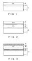
- a layer 5 which is either a layer consisting of polycyclic aromatic group molecules or a derivative thereof or a carbon layer having a graphite structure is formed on the surface of a substrate main body 11, and an organic thin film layer 12 is formed thereon.
- the organic thin film element shown in Fig. 2 has a superlattice structure in that a layer 5 consisting of polycyclic aromatic group molecules or a derivative thereof is formed on the surface of a substrate main body 11, and a first organic thin film layer 12, a layer 5 consisting of a polycyclic aromatic group molecules or a derivative thereof, and a second organic thin film layer 13 are sequentially formed thereon.
- an electrode 2 an insulating layer 3, and a layer which is either a layer consisting of polycyclic aromatic group molecules or a derivative thereof or a carbon layer 5 having a graphite structure are formed on the surface of a substrate main body 11, and an organic thin film layer 12, an insulating layer 14, and a back electrode 15 are sequentially formed.
- a decacyclene film having a film thickness of about 10 nm was formed on an Si substrate main body at a substrate temperature of 50°C by a vacuum deposition method.
- a TCNQ film having a film thickness of about 100 nm was formed on the resultant substrate by the vacuum deposition method.
- a violanthrene film having a film thickness of about 5 nm was formed on an Si substrate main body at a substrate temperature of 55°C by the vacuum deposition method.
- a phthalocyanine film having a film thickness of about 500 nm was formed on the resultant substrate by the vacuum deposition method.
- a violanthrene film having a film thickness of about 5 nm was formed on an Si substrate main body at a substrate temperature of 55°C by the vacuum deposition method.
- a phenothiazine-TCNQ film having a film thickness of about 10 nm was formed on the resultant substrate by the vacuum deposition method.
- a violanthrene film having a film thickness of about 5 nm was formed on an Si substrate main body at a substrate temperature of 55°C by the vacuum deposition method.
- a TCNQ film having a film thickness of about 100 nm, a violanthrene film having a film thickness of about 5 nm, and a phenothiazine-TCNQ film having a film thickness of about 10 nm were formed on the resultant substrate by the vacuum deposition method.
- An Si substrate main body was dipped in a toluene solution of coronene and heated at 80°C to evaporate the solvent, thereby forming a coronene film.
- a phenothiazine-TCNQ film having a film thickness of about 30 nm was formed on the resultant substrate at a substrate temperature of 50°C by the vacuum deposition method.
- An Si substrate main body was dipped in a toluene solution of coronene and heated at 80°C to evaporate the solvent, thereby forming a coronene film.
- a violanthrene film having a film thickness of 2 nm and a phenothiazine-TCNQ film having a film thickness of about 30 nm were formed on the resultant substrate at a substrate temperature of 50°C by the vacuum deposition method.
- An ITO transparent electrode having a film thickness of 400 nm and an SiO2 film having a film thickness of 200 nm as an insulating layer were formed on a quartz substrate main body.
- the resultant substrate was dipped in a toluene solution of coronene and heated at 80°C to evaporate the solvent, thereby forming a coronene film.
- a violanthrene film having a film thick ness of 2 nm and a phenothiazine-TCNQ film having a film thickness of about 30 nm were formed on the substrate at a substrate temperature of 50°C by the vacuum deposition method.
- a polyisobutylmethacrylate film having a film thickness of 20 nm as an insulating layer and an Au semitransparent electrode having a film thickness of 25 nm were formed on the phenothiazine-TCNQ film to manufacture an organic thin film element.
- the organic thin film layer of this element When no voltage was applied, the organic thin film layer of this element exhibited an orange color. When a voltage was applied to the organic thin film layer, the color of the layer changed to dark red at a voltage of about 30 V.
- An Si substrate main body was left to stand in a hexamethyldisilazane vapor phase for a hydrophobic treatment.
- a monomolecular film containing tetra t-butylphthalocyanine and octadecane at a mixing ratio of 1 : 4 was developed on a water surface, and three layers of this monomolecular film were accumulated on the substrate main body.
- a phenothiazine-TCNQ film having a film thickness of about 30 nm was formed on the resultant substrate at a substrate temperature of 50°C by the vacuum deposition method.
- An Si substrate main body was left to stand in a hexamethyldisilazane vapor phase for a hydrophobic treatment.
- a monomolecular film containing tetra t-butylphthalocyanine and octadecane at a mixing ratio of 1 : 4 was developed on a water surface, and three layers of this monomolecular film were accumulated on the substrate main body.
- a violanthrene film having a film thickness of 3 nm and a phenothiazine-TCNQ film having a film thickness of about 30 nm were formed on the resultant substrate at a substrate temperature of 55°C by the vacuum deposition method.
- An ITO transparent electrode having a film thickness of 400 nm and an SiO2 film having a film thickness of 200 nm as an insulating layer were formed on a quartz substrate main body.
- a monomolecular film containing tetra t-butylphthalocyanine and octadecane at a mixing ratio of 1 : 4 was developed on a water surface, and three layers of this monomolecular film were accumulated on the resultant substrate.
- a violanthrene film having a film thickness of 3 nm and a phenothiazine-TCNQ film having a film thickness of about 30 nm were formed on the substrate at a substrate temperature of 55°C by the vacuum deposition method.
- a polyisobutylmethacrylate film having a film thickness of 20 nm as an insulating layer and an Au semitransparent electrode having a film thickness of 25 nm were formed on the phenothiazine-TCNQ film to manufacture an organic thin film element.
- the organic thin film layer of this element When no voltage was applied, the organic thin film layer of this element exhibited an orange color. When a voltage was applied to the organic thin film layer, the color of the layer changed to dark red at a voltage of about 30 V.
- An Si substrate main body was left to stand in a bistrichlorosilylpyrene vapor phase for a surface treatment.
- a TTF-chloranil film having a film thickness of about 30 nm was formed on the resultant substrate by the vacuum deposition method.
- An ITO transparent electrode having a film thickness of 400 nm and an SiO2 film having a film thickness of 150 nm as an insulating layer were formed on a quartz substrate main body.
- the resultant substrate was subjected to a surface treatment in a bistrichlorosilylpyrene vapor phase.
- a TTF-chloranil film having a film thickness of about 30 nm was formed on the substrate by the vacuum deposition method.
- a polyisobutylmethacrylate film having a film thickness of 20 nm as an insulating layer and an Au semitransparent electrode having a film thickness of 20 nm were formed on the TTF-chloranil film to manufacture an organic thin film element.
- the organic thin film layer of this element When no voltage was applied, the organic thin film layer of this element exhibited a yellow color. When a voltage was applied to the organic thin film layer, the color of the layer changed to red at a voltage of about 50 V.
- An ITO transparent electrode having a film thickness of 400 nm and an SrTiO3 film having a film thickness of 200 nm as an insulating layer were formed on a quartz substrate main body.
- the resultant substrate was subjected to a surface treatment in a bistrichlorosilylpyrene vapor phase.
- a TTF-chloranil film having a film thickness of about 30 nm was formed on the substrate by the vacuum deposition method.
- a polyisobutylmethacrylate film having a film thickness of 20 nm as an insulating layer and an Au semitransparent electrode having a film thickness of 20 nm were formed on the TTF-chloranil film to manufacture an organic thin film element.
- the organic thin film layer of this element When no voltage was applied, the organic thin film layer of this element exhibited a yellow color. When a voltage was applied to the organic thin film layer, the color of the layer changed to red at a voltage of about 25 V.
- An Si substrate main body was subjected to a surface treatment in a ⁇ -aminopropyltriethoxysilane vapor phase.
- Perylenetetracarboxylic dianhydride was deposited on the resultant substrate by the vacuum deposition method, and the substrate was heated up to about 70°C to cause a condensation reaction and redissociation of non-condensed molecules. Thereafter, a TTF-chloranil film having a film thickness of about 30 nm was formed.
- An ITO transparent electrode having a film thickness of 400 nm and an SiO2 film having a film thickness of 150 nm as an insulating layer were formed on a quartz substrate main body.
- the resultant substrate was subjected to a surface treatment in a ⁇ -aminopropyltriethoxysilane vapor phase.
- Perylenetetracarboxylic dianhydride was deposited on the resultant substrate by the vacuum deposition method, and the substrate was heated up to about 70°C to cause a condensation reaction and re-dissociation of non-condensed molecules. Thereafter, a TTF-chloranil film having a film thickness of about 30 nm was formed.
- a polyisobutylmethacrylate film having a film thickness of 20 nm as an insulating layer and an Au semitransparent electrode having a film thickness of 20 nm were formed on the TTF-chloranil film to manufacture an organic thin film element.
- the organic thin film layer of this organic thin film element exhibited a yellow color.
- the color of the layer changed to red at a voltage of about 50 V.
- An ITO transparent electrode having a film thickness of 400 nm and an SrTiO3 film having a film thickness of 200 nm as an insulating layer were formed on a quartz substrate main body.
- the resultant substrate was subjected to a surface treatment in a y-aminopropyltriethoxysilane vapor phase.
- Perylenetetracarboxylic dianhydride was deposited on the resultant substrate by the vacuum deposition method, and the substrate was heated up to about 70°C to cause a condensation reaction and re-dissociation of non-condensed molecules. Thereafter, a TTF-chloranil film having a film thickness of about 30 nm was formed.
- a polyisobutylmethacrylate film having a film thickness of 20 nm as an insulating layer and an Au semitransparent electrode having a film thickness of 20 nm were formed on the TTF-chloranil film to manufacture an organic thin film element.
- the organic thin film layer of this element When no voltage was applied, the organic thin film layer of this element exhibited a yellow color. When a voltage was applied to the organic thin film layer, the color of the layer changed to red at a voltage of about 25 V.
- a perylenetetracarboxylic dianhydride film having a film thickness of 20 nm was formed on an Si substrate main body, and the resultant substrate was heated up to 550°C in an argon atmosphere. As a result, most of the film changed to polyperynaphthalene.
- a phenothiazine-TCNQ film having a film thickness of about 30 nm was formed on the resultant substrate at a substrate temperature of 50°C by the vacuum deposition method.
- a perylenetetracarboxylic dianhydride film having a film thickness of 20 nm was formed on an Si substrate main body, and the resultant substrate was heated up to 550°C in an argon atmosphere. As a result, most of the film changed to polyperynaphthalene.
- a violanthrene film having a film thickness of about 2 nm and a phenothiazine-TCNQ film having a film thickness of about 30 nm were formed on the resultant substrate at a substrate temperature of 50°C by the vacuum deposition method.
- An ITO transparent electrode having a film thickness of 400 nm and an SiO2 film having a film thickness of 200 nm as an insulating layer were formed on a quartz substrate main body.
- a perylenetetracarboxylic dianhydride film having a film thickness of 20 nm was formed on the resultant substrate, and the substrate was heated up to 550°C in an argon atmosphere. As a result, most of the film changed to polyperynaphthalene.
- a violanthrene film having a film thickness of about 3 nm and a phenothiazine-TCNQ film having a film thickness of about 30 nm were formed on the resultant substrate at a substrate temperature of 50°C by the vacuum deposition method.
- a polyisobutylmethacrylate film having a film thickness of 20 nm as an insulating layer and an Au semitransparent electrode having a film thickness of 25 nm were formed on the phenothiazine-TCNQ film to manufacture an organic thin film element.
- the organic thin film layer of this element When no voltage was applied, the organic thin film layer of this element exhibited an orange color. When a voltage was applied to the organic thin film layer, the color of the layer changed to dark red at a voltage of about 30 V.
- An ITO transparent electrode having a film thickness of 400 nm and an SiO2 film having a film thickness of 200 nm as an insulating layer were formed on a quartz substrate main body.
- a co-deposition film consisting of ovalene and 1,4-benzenedimethylchloride was formed on the resultant substrate, and a polycondensation film was formed in an argon atmosphere containing PCl5 at a substrate temperature of 150°C.
- a violanthrene film having a film thickness of about 2 nm and a phenothiazine-TCNQ film having a film thickness of about 30 nm were formed on the resultant substrate at a substrate temperature of 50°C by the vacuum deposition method.
- a polyisobutylmethacrylate film having a film thickness of 20 nm as an insulating layer and an Au semitransparent electrode having a film thickness of 25 nm were formed on the phenothiazine-TCNQ film to manufacture an organic thin film element.
- the organic thin film layer of this element When no voltage was applied, the organic thin film layer of this element exhibited an orange color. When a voltage was applied to the organic thin film layer, the color of the layer changed to dark red at a voltage of about 30 V.
- An ITO transparent electrode having a film thickness of 400 nm and an SiO2 film having a film thickness of 200 nm as an insulating layer were formed on a quartz substrate main body.
- a polyoxadiazole film was formed on the resultant substrate by a cast method, and the substrate was subjected to a heat treatment at 900°C in a vacuum.
- a violanthrene film having a film thickness of about 2 nm and a phenothiazine-TCNQ film having a film thickness of about 30 nm were formed on the resultant substrate at a substrate temperature of 50°C by the vacuum deposition method.
- a polyisobutylmethacrylate film having a film thickness of 20 nm as an insulating layer and an Au semitransparent electrode having a film thickness of 25 nm were formed on the phenothiazine-TCNQ film to manufacture an organic thin film element.
- the organic thin film layer of this element When no voltage was applied, the organic thin film layer of this element exhibited an orange color. When a voltage was applied to the organic thin film layer, the color of the layer changed to dark red at a voltage of about 30 V.
- a perylenetetracarboxylic dianhydride film having a film thickness of 50 nm was formed on an Si substrate main body, and an argon ion beam was radiated at an acceleration energy of 3 MeV and a dose of 1016cm ⁇ 2 in a vacuum.
- a phenothiazine-TCNQ film having a film thickness of about 30 nm was formed on the resultant substrate at a substrate temperature of 50°C by the vacuum deposition method.
- a perylenetetracarboxylic dianhydride film having a film thickness of 50 nm was formed on an Si substrate main body, and an argon ion beam was radiated at an acceleration energy of 3 MeV and a dose of 1016 cm ⁇ 2 in a vacuum.
- a violanthrene film having a film thickness of 2 nm and a phenothiazine-TCNQ film having a film thickness of about 30 nm was formed on the resultant substrate at a substrate temperature of 50°C by the vacuum deposition method.
- An ITO transparent electrode having a film thickness of 400 nm and an SiO2 film having a film thickness of 200 nm as an insulating layer were formed on a quartz substrate main body.
- a perylenetetracarboxylic dianhydride film having a film thickness of 50 nm was formed on the resultant substrate, and an argon ion beam was radiated at an acceleration energy of 3 MeV and a dose of 1016 cm ⁇ 2 in a vacuum.
- a violanthrene film having a film thickness of 2 nm and a phenothiazine-TCNQ film having a film thickness of about 30 nm were formed on the resultant substrate at a substrate temperature of 50°C by the vacuum deposition method.
- a polyisobutylmethacrylate film having a film thickness of 20 nm as an insulating layer and an Au semitransparent electrode having a film thickness of 25 nm were formed on the phenothiazine-TCNQ film to manufacture an organic thin film element.
- the organic thin film layer of this element When no voltage was applied, the organic thin film layer of this element exhibited an orange color. When a voltage was applied to the organic thin film layer, the color of the layer changed to dark red at a voltage of about 30 V.
- a diindenoperylene film having a film thickness of 50 nm was formed on an Si substrate main body, and an electron beam was radiated at an acceleration voltage of 20 kV.
- a violanthrene film having a film thickness of 2 nm and a phenothiazine-TCNQ film having a film thickness of about 30 nm was formed on the resultant substrate at a substrate temperature of 50°C by the vacuum deposition method.
- An ITO transparent electrode having a film thickness of 400 mn and an SiO2 film having a film thickness of 200 nm as an insulating layer were formed on a quartz substrate main body.
- a diindenoperylene film having a film thickness of 50 nm was formed on the resultant substrate, and an electron beam was radiated at an acceleration voltage of 20 kV.
- a violanthrene film having a film thickness of 2 nm and a phenothiazine-TCNQ film having a film thickness of about 30 nm were formed on the resultant substrate at a substrate temperature of 50°C by the vacuum deposition method.
- a polyisobutylmethacrylate film having a film thickness of 20 nm as an insulating layer and an Au semitransparent electrode having a film thickness of 25 nm were formed on the phenothiazine-TCNQ film to manufacture an organic thin film element.
- the organic thin film layer of this element When no voltage was applied, the organic thin film layer of this element exhibited an orange color. When a voltage was applied to the organic thin film layer, the color of the layer changed to dark red at a voltage of about 30 V.
- An ITO transparent electrode having a film thickness of 400 nm and an SiO2 film having a film thickness of 200 nm as an insulating layer were formed on a quartz substrate main body.
- a perylenetetracarboxylic dianhydride film having a film thickness of 50 nm was formed on the resultant substrate, and an electron beam was radiated at an acceleration voltage of 20 kV to form a rectangular pattern.
- the resultant substrate was dipped in tetrahydrofuran to dissolve a film at a non-radiated portion.
- a violanthrene film having a film thickness of 2 nm and a phenothiazine-TCNQ film having a film thickness of about 30 nm were formed on the resultant substrate at a substrate temperature of 50°C by the vacuum deposition method.
- a polyisobutylmethacrylate film having a film thickness of 20 nm as an insulating layer and an Au semitransparent electrode having a film thickness of 25 nm were formed on the phenothianize-TCNQ film to manufacture an organic thin film element.
- the organic thin film layer on the region on which the perylenetetracarboxylic dianhydride film was patterned exhibited an orange color.
- the color of the layer on the same region changed to dark red at a voltage of about 30 V.
- An Ni film having a film thickness of 50 nm was formed on an Si substrate main body by an electron beam deposition method.
- the resultant substrate was exposed to ethylene gas for 150 to 300 Langmuir (to be abbreviated to as L hereinafter) or more while being heated up to 850°C, thereby forming a carbon layer similar to graphite on its surface.
- a TCNQ film having a film thickness of about 100 nm was formed on the resultant substrate by the vacuum deposition method.
- a TiC film having a film thickness of 20 nm was formed on an Si substrate main body by a CVD method.
- the resultant substrate was exposed to ethylene gas for 150 to 300 L or more while being heated up to 850°C, thereby forming a carbon layer similar to graphite on its surface.
- a TCNQ film having a film thickness of about 100 nm was formed on the resultant substrate by the vacuum deposition method.
- An SiO2 film having a film thickness of 20 nm was formed on the surface of an Si substrate main body by a thermal oxidation method.
- a TiC film having a film thickness of 20 nm was formed on one surface of the resultant substrate by the CVD method.
- the resultant substrate was exposed to ethylene gas for 150 to 300 L or more while being heated up to 850°C, thereby forming a carbon layer similar to graphite on the TiC film.
- a methylphenazine-TCNQ film having a film thickness of about 30 nm was formed on the resultant substrate by the vacuum deposition method.
- a polyisobutylmethacrylate film having a film thickness of 20 nm as an insulating layer and an Au semitransparent electrode having a film thickness of 25 nm were formed on the methylphenazine-TCNQ film to manufacture an organic thin film element.
Landscapes
- Physics & Mathematics (AREA)
- Engineering & Computer Science (AREA)
- Chemical & Material Sciences (AREA)
- Nonlinear Science (AREA)
- General Physics & Mathematics (AREA)
- Nanotechnology (AREA)
- Materials Engineering (AREA)
- Crystallography & Structural Chemistry (AREA)
- Condensed Matter Physics & Semiconductors (AREA)
- Optics & Photonics (AREA)
- Composite Materials (AREA)
- Manufacturing & Machinery (AREA)
- Spectroscopy & Molecular Physics (AREA)
- Physical Vapour Deposition (AREA)
Applications Claiming Priority (3)
| Application Number | Priority Date | Filing Date | Title |
|---|---|---|---|
| JP7541390 | 1990-03-27 | ||
| JP75413/90 | 1990-03-27 | ||
| JP7541390 | 1990-03-27 |
Publications (3)
| Publication Number | Publication Date |
|---|---|
| EP0450862A2 true EP0450862A2 (de) | 1991-10-09 |
| EP0450862A3 EP0450862A3 (de) | 1994-10-12 |
| EP0450862B1 EP0450862B1 (de) | 1999-06-30 |
Family
ID=13575464
Family Applications (1)
| Application Number | Title | Priority Date | Filing Date |
|---|---|---|---|
| EP91302714A Expired - Lifetime EP0450862B1 (de) | 1990-03-27 | 1991-03-27 | Dünnes organisches Filmelement |
Country Status (2)
| Country | Link |
|---|---|
| US (1) | US5155566A (de) |
| EP (1) | EP0450862B1 (de) |
Cited By (5)
| Publication number | Priority date | Publication date | Assignee | Title |
|---|---|---|---|---|
| WO2000042668A1 (en) * | 1999-01-15 | 2000-07-20 | The Dow Chemical Company | Semiconducting polymer field effect transistor |
| WO2001001502A2 (en) * | 1999-06-30 | 2001-01-04 | Thin Film Electronics Asa | A means for electrical contacting or isolation of organic or inorganic semiconductors and a method for its fabrication |
| WO2005034172A2 (de) * | 2003-09-30 | 2005-04-14 | Infineon Technologies Ag | Material und zellenaufbau für speicheranwendungen |
| DE102004004863A1 (de) * | 2004-01-30 | 2005-09-01 | Infineon Technologies Ag | Resistiv arbeitender Speicher |
| EP1737045A1 (de) * | 2004-03-24 | 2006-12-27 | Japan Science and Technology Agency | Substrat mit organischem dünnfilm, transistor damit und herstellungsverfahren dafür |
Families Citing this family (21)
| Publication number | Priority date | Publication date | Assignee | Title |
|---|---|---|---|---|
| JP2814024B2 (ja) * | 1990-06-07 | 1998-10-22 | キヤノン株式会社 | 液晶素子 |
| US6559469B1 (en) * | 1992-10-23 | 2003-05-06 | Symetrix Corporation | Ferroelectric and high dielectric constant transistors |
| US5682043A (en) * | 1994-06-28 | 1997-10-28 | Uniax Corporation | Electrochemical light-emitting devices |
| US5663573A (en) * | 1995-03-17 | 1997-09-02 | The Ohio State University | Bipolar electroluminescent device |
| WO1996037001A1 (en) * | 1995-05-19 | 1996-11-21 | Uniax Corporation | Electrochemical light-emitting devices |
| US5677546A (en) * | 1995-05-19 | 1997-10-14 | Uniax Corporation | Polymer light-emitting electrochemical cells in surface cell configuration |
| US5849403A (en) * | 1995-09-13 | 1998-12-15 | Kabushiki Kaisha Toshiba | Organic thin film device |
| US5943154A (en) * | 1996-09-17 | 1999-08-24 | Kabushiki Kaisha Toshiba | Optically-controlled light control element |
| US6316098B1 (en) | 1998-03-27 | 2001-11-13 | Yissum Research Development Company Of The Hebrew University Of Jerusalem | Molecular layer epitaxy method and compositions |
| US6783849B2 (en) * | 1998-03-27 | 2004-08-31 | Yissum Research Development Company Of The Hebrew University Of Jerusalem | Molecular layer epitaxy method and compositions |
| US6542320B1 (en) * | 1998-05-05 | 2003-04-01 | Niermann Weeks Company, Inc. | Mirror and antiquing process for producing the mirror |
| US6284562B1 (en) * | 1999-11-17 | 2001-09-04 | Agere Systems Guardian Corp. | Thin film transistors |
| JP4103421B2 (ja) * | 2001-03-28 | 2008-06-18 | セイコーエプソン株式会社 | 電子デバイス及び電子機器 |
| JP4076749B2 (ja) * | 2001-10-15 | 2008-04-16 | 富士フイルム株式会社 | 導電性有機化合物及び電子素子 |
| US6902831B2 (en) | 2002-11-26 | 2005-06-07 | Canon Kabushiki Kaisha | Azulene-based compounds in organic light emitting device elements |
| JP4243237B2 (ja) * | 2003-11-10 | 2009-03-25 | 淳二 城戸 | 有機素子、有機el素子、有機太陽電池、及び、有機fet構造、並びに、有機素子の製造方法 |
| WO2007005618A2 (en) * | 2005-06-30 | 2007-01-11 | The Regents Of The University Of California | High performance organic thin film transistor |
| US7619257B2 (en) * | 2006-02-16 | 2009-11-17 | Alcatel-Lucent Usa Inc. | Devices including graphene layers epitaxially grown on single crystal substrates |
| US8043978B2 (en) * | 2007-10-11 | 2011-10-25 | Riken | Electronic device and method for producing electronic device |
| KR102167041B1 (ko) * | 2013-08-14 | 2020-10-19 | 삼성디스플레이 주식회사 | 헤테로고리 화합물 및 이를 포함한 유기 발광 소자 |
| CN113471365B (zh) * | 2021-05-13 | 2023-10-27 | 中国计量大学 | 近红外有机范德华异质结光敏场效应晶体管及其制备方法 |
Citations (5)
| Publication number | Priority date | Publication date | Assignee | Title |
|---|---|---|---|---|
| FR2321770A1 (fr) * | 1975-08-18 | 1977-03-18 | Ici Ltd | Procede pour preparer des dispositifs composites comportant des pellicules minces a fort degre d'orientation moleculaire |
| US4164431A (en) * | 1977-08-02 | 1979-08-14 | Eastman Kodak Company | Multilayer organic photovoltaic elements |
| US4214916A (en) * | 1979-02-05 | 1980-07-29 | Arthur Bradley | Thin film photovoltaic converter and method of preparing same |
| EP0215683A2 (de) * | 1985-09-18 | 1987-03-25 | Kabushiki Kaisha Toshiba | Organisches Dünnschicht-Bildwiedergabeelement |
| EP0344108A2 (de) * | 1988-05-27 | 1989-11-29 | Ciba-Geigy Ag | Elektroaktive ultradünne Schichten |
Family Cites Families (1)
| Publication number | Priority date | Publication date | Assignee | Title |
|---|---|---|---|---|
| DE3667581D1 (de) * | 1985-03-22 | 1990-01-18 | Kanegafuchi Chemical Ind | Elektrolumineszente vorrichtung. |
-
1991
- 1991-03-27 US US07/675,964 patent/US5155566A/en not_active Expired - Lifetime
- 1991-03-27 EP EP91302714A patent/EP0450862B1/de not_active Expired - Lifetime
Patent Citations (5)
| Publication number | Priority date | Publication date | Assignee | Title |
|---|---|---|---|---|
| FR2321770A1 (fr) * | 1975-08-18 | 1977-03-18 | Ici Ltd | Procede pour preparer des dispositifs composites comportant des pellicules minces a fort degre d'orientation moleculaire |
| US4164431A (en) * | 1977-08-02 | 1979-08-14 | Eastman Kodak Company | Multilayer organic photovoltaic elements |
| US4214916A (en) * | 1979-02-05 | 1980-07-29 | Arthur Bradley | Thin film photovoltaic converter and method of preparing same |
| EP0215683A2 (de) * | 1985-09-18 | 1987-03-25 | Kabushiki Kaisha Toshiba | Organisches Dünnschicht-Bildwiedergabeelement |
| EP0344108A2 (de) * | 1988-05-27 | 1989-11-29 | Ciba-Geigy Ag | Elektroaktive ultradünne Schichten |
Non-Patent Citations (2)
| Title |
|---|
| THIN SOLID FILMS, vol.152, September 1987, LAUSANNE CH pages 305 - 326, XP21379 MICHIO SUGI 'Molecular Engineering in Japan - A Prospect of research on Langmuir-Blodgett films' * |
| THIN SOLID FILMS, vol.179, no.1, 11 November 1989, LAUSANNE CH pages 471 - 476, XP99681 MASAMICHI FUJIHIRA ET AL. 'Photoinduced intramolecular electron transfer across monolayers consisting of linear A-S-D triad amphiphilic molecules' * |
Cited By (11)
| Publication number | Priority date | Publication date | Assignee | Title |
|---|---|---|---|---|
| WO2000042668A1 (en) * | 1999-01-15 | 2000-07-20 | The Dow Chemical Company | Semiconducting polymer field effect transistor |
| US6204515B1 (en) | 1999-01-15 | 2001-03-20 | The Dow Chemical Company | Semiconducting polymer field effect transistor |
| WO2001001502A2 (en) * | 1999-06-30 | 2001-01-04 | Thin Film Electronics Asa | A means for electrical contacting or isolation of organic or inorganic semiconductors and a method for its fabrication |
| WO2001001502A3 (en) * | 1999-06-30 | 2001-03-22 | Thin Film Electronics Asa | A means for electrical contacting or isolation of organic or inorganic semiconductors and a method for its fabrication |
| WO2005034172A2 (de) * | 2003-09-30 | 2005-04-14 | Infineon Technologies Ag | Material und zellenaufbau für speicheranwendungen |
| WO2005034172A3 (de) * | 2003-09-30 | 2005-08-18 | Infineon Technologies Ag | Material und zellenaufbau für speicheranwendungen |
| DE102004004863A1 (de) * | 2004-01-30 | 2005-09-01 | Infineon Technologies Ag | Resistiv arbeitender Speicher |
| DE102004004863B4 (de) * | 2004-01-30 | 2007-01-25 | Infineon Technologies Ag | Resistiv arbeitende Speicherzelle |
| US7238964B2 (en) | 2004-01-30 | 2007-07-03 | Infineon Technologies Ag | Memory cell, method for the production thereof and use of a composition therefor |
| EP1737045A1 (de) * | 2004-03-24 | 2006-12-27 | Japan Science and Technology Agency | Substrat mit organischem dünnfilm, transistor damit und herstellungsverfahren dafür |
| EP1737045A4 (de) * | 2004-03-24 | 2012-02-29 | Japan Science & Tech Agency | Substrat mit organischem dünnfilm, transistor damit und herstellungsverfahren dafür |
Also Published As
| Publication number | Publication date |
|---|---|
| US5155566A (en) | 1992-10-13 |
| EP0450862B1 (de) | 1999-06-30 |
| EP0450862A3 (de) | 1994-10-12 |
Similar Documents
| Publication | Publication Date | Title |
|---|---|---|
| EP0450862B1 (de) | Dünnes organisches Filmelement | |
| Khodabakhsh et al. | Using self‐assembling dipole molecules to improve hole injection in conjugated polymers | |
| Fahlman et al. | Surfaces and interfaces in polymer-based electronics | |
| Osada et al. | Polymer-based light-emitting devices: investigations on the role of the indium—tin oxide (ITO) electrode | |
| US7061011B2 (en) | Bipolar organic devices | |
| US5854139A (en) | Organic field-effect transistor and production thereof | |
| JP2001189466A (ja) | スイッチング素子の製造方法、スイッチング素子及びスイッチング素子アレイ | |
| TWI229572B (en) | Organic EL light emitting device and liquid crystal display using the same | |
| Chen et al. | Polarized electroluminescence from aligned chromophores by the friction transfer method | |
| Carrard et al. | Improved stability of interfaces in organic light emitting diodes with high Tg materials and self-assembled monolayers | |
| Zhang et al. | Constructing Effective Hole Transport Channels in Cross‐Linked Hole Transport Layer by Stacking Discotic Molecules for High Performance Deep Blue QLEDs | |
| Yoshizaki et al. | Large surface potential of Alq3 film and its decay | |
| WO2007094164A1 (ja) | 有機薄膜トランジスタ及びその製造方法 | |
| Lei et al. | Highly efficient and bright red quantum dot light-emitting diodes with balanced charge injection | |
| Hu et al. | Highly ordered vacuum-deposited thin films of copper phthalocyanine induced by electric field | |
| JP4006951B2 (ja) | 有機電界発光素子およびその製造方法 | |
| JP4030608B2 (ja) | 有機電界発光素子及びその製造方法 | |
| JP3750315B2 (ja) | 有機電界発光素子 | |
| JP3302703B2 (ja) | 有機薄膜素子 | |
| JP5025124B2 (ja) | 有機半導体装置及びその製造方法並びに表示装置 | |
| Zhou et al. | Synthetic Molecular Rectifier of a Langmuir–Blodgett Film Based on a Novel Asymmetrically Substituted Dicyano‐tri‐tert‐butylphthalocyanine | |
| JP2004158709A (ja) | 半導体装置 | |
| JP5000516B2 (ja) | トンネリング用ダスト電極を有するトランジスター | |
| Takagi et al. | Metal patterning using maskless vacuum evaporation process based on selective deposition of photochromic diarylethene | |
| WO2007129643A1 (ja) | 有機半導体材料を用いた電界効果トランジスタおよびその製造方法 |
Legal Events
| Date | Code | Title | Description |
|---|---|---|---|
| PUAI | Public reference made under article 153(3) epc to a published international application that has entered the european phase |
Free format text: ORIGINAL CODE: 0009012 |
|
| 17P | Request for examination filed |
Effective date: 19910412 |
|
| AK | Designated contracting states |
Kind code of ref document: A2 Designated state(s): DE FR GB |
|
| PUAL | Search report despatched |
Free format text: ORIGINAL CODE: 0009013 |
|
| AK | Designated contracting states |
Kind code of ref document: A3 Designated state(s): DE FR GB |
|
| 17Q | First examination report despatched |
Effective date: 19960716 |
|
| GRAG | Despatch of communication of intention to grant |
Free format text: ORIGINAL CODE: EPIDOS AGRA |
|
| GRAG | Despatch of communication of intention to grant |
Free format text: ORIGINAL CODE: EPIDOS AGRA |
|
| GRAH | Despatch of communication of intention to grant a patent |
Free format text: ORIGINAL CODE: EPIDOS IGRA |
|
| GRAH | Despatch of communication of intention to grant a patent |
Free format text: ORIGINAL CODE: EPIDOS IGRA |
|
| REG | Reference to a national code |
Ref country code: DE Ref legal event code: 8566 |
|
| GRAA | (expected) grant |
Free format text: ORIGINAL CODE: 0009210 |
|
| AK | Designated contracting states |
Kind code of ref document: B1 Designated state(s): GB |
|
| PLBE | No opposition filed within time limit |
Free format text: ORIGINAL CODE: 0009261 |
|
| STAA | Information on the status of an ep patent application or granted ep patent |
Free format text: STATUS: NO OPPOSITION FILED WITHIN TIME LIMIT |
|
| 26N | No opposition filed | ||
| REG | Reference to a national code |
Ref country code: GB Ref legal event code: IF02 |
|
| PGFP | Annual fee paid to national office [announced via postgrant information from national office to epo] |
Ref country code: GB Payment date: 20080402 Year of fee payment: 18 |
|
| GBPC | Gb: european patent ceased through non-payment of renewal fee |
Effective date: 20090327 |
|
| PG25 | Lapsed in a contracting state [announced via postgrant information from national office to epo] |
Ref country code: GB Free format text: LAPSE BECAUSE OF NON-PAYMENT OF DUE FEES Effective date: 20090327 |