EP0447096B1 - Quantenstruktur-Laser mit einer InGaAsP-Begrenzungsschicht und Verfahren zur Herstellung des Lasers - Google Patents
Quantenstruktur-Laser mit einer InGaAsP-Begrenzungsschicht und Verfahren zur Herstellung des Lasers Download PDFInfo
- Publication number
- EP0447096B1 EP0447096B1 EP91301801A EP91301801A EP0447096B1 EP 0447096 B1 EP0447096 B1 EP 0447096B1 EP 91301801 A EP91301801 A EP 91301801A EP 91301801 A EP91301801 A EP 91301801A EP 0447096 B1 EP0447096 B1 EP 0447096B1
- Authority
- EP
- European Patent Office
- Prior art keywords
- laser
- active region
- confinement layer
- composition
- strained
- Prior art date
- Legal status (The legal status is an assumption and is not a legal conclusion. Google has not performed a legal analysis and makes no representation as to the accuracy of the status listed.)
- Expired - Lifetime
Links
- 238000000034 method Methods 0.000 title claims description 12
- 239000000203 mixture Substances 0.000 claims description 43
- 239000000463 material Substances 0.000 claims description 18
- 230000005855 radiation Effects 0.000 claims description 16
- 239000000835 fiber Substances 0.000 claims description 13
- 239000004065 semiconductor Substances 0.000 claims description 11
- 239000013307 optical fiber Substances 0.000 claims description 10
- 230000004888 barrier function Effects 0.000 claims description 8
- 230000003287 optical effect Effects 0.000 claims description 8
- 230000015572 biosynthetic process Effects 0.000 claims description 5
- 238000004891 communication Methods 0.000 claims description 5
- 238000004519 manufacturing process Methods 0.000 claims description 5
- 230000008878 coupling Effects 0.000 claims description 3
- 238000010168 coupling process Methods 0.000 claims description 3
- 238000005859 coupling reaction Methods 0.000 claims description 3
- 230000008859 change Effects 0.000 description 16
- XCZXGTMEAKBVPV-UHFFFAOYSA-N trimethylgallium Chemical compound C[Ga](C)C XCZXGTMEAKBVPV-UHFFFAOYSA-N 0.000 description 11
- 230000007547 defect Effects 0.000 description 10
- RBFQJDQYXXHULB-UHFFFAOYSA-N arsane Chemical compound [AsH3] RBFQJDQYXXHULB-UHFFFAOYSA-N 0.000 description 9
- 229910000070 arsenic hydride Inorganic materials 0.000 description 9
- IBEFSUTVZWZJEL-UHFFFAOYSA-N trimethylindium Chemical compound C[In](C)C IBEFSUTVZWZJEL-UHFFFAOYSA-N 0.000 description 7
- 241000894007 species Species 0.000 description 5
- 229910000980 Aluminium gallium arsenide Inorganic materials 0.000 description 4
- 229910001218 Gallium arsenide Inorganic materials 0.000 description 3
- 229910000530 Gallium indium arsenide Inorganic materials 0.000 description 3
- 239000002243 precursor Substances 0.000 description 3
- QVGXLLKOCUKJST-UHFFFAOYSA-N atomic oxygen Chemical compound [O] QVGXLLKOCUKJST-UHFFFAOYSA-N 0.000 description 2
- 230000005540 biological transmission Effects 0.000 description 2
- 230000002939 deleterious effect Effects 0.000 description 2
- 230000000694 effects Effects 0.000 description 2
- 239000007789 gas Substances 0.000 description 2
- 229910052760 oxygen Inorganic materials 0.000 description 2
- 239000001301 oxygen Substances 0.000 description 2
- 238000005086 pumping Methods 0.000 description 2
- 229910052761 rare earth metal Inorganic materials 0.000 description 2
- 150000002910 rare earth metals Chemical class 0.000 description 2
- 239000000758 substrate Substances 0.000 description 2
- 230000003321 amplification Effects 0.000 description 1
- 229910052785 arsenic Inorganic materials 0.000 description 1
- 239000011248 coating agent Substances 0.000 description 1
- 238000000576 coating method Methods 0.000 description 1
- 238000007796 conventional method Methods 0.000 description 1
- 239000013078 crystal Substances 0.000 description 1
- 230000003247 decreasing effect Effects 0.000 description 1
- 230000006866 deterioration Effects 0.000 description 1
- 230000008030 elimination Effects 0.000 description 1
- 238000003379 elimination reaction Methods 0.000 description 1
- 229910052733 gallium Inorganic materials 0.000 description 1
- 238000000171 gas-source molecular beam epitaxy Methods 0.000 description 1
- 230000017525 heat dissipation Effects 0.000 description 1
- 229910052738 indium Inorganic materials 0.000 description 1
- 229910052751 metal Inorganic materials 0.000 description 1
- 239000002184 metal Substances 0.000 description 1
- 238000002488 metal-organic chemical vapour deposition Methods 0.000 description 1
- 238000003199 nucleic acid amplification method Methods 0.000 description 1
- 230000008569 process Effects 0.000 description 1
- 229910002059 quaternary alloy Inorganic materials 0.000 description 1
- 230000004044 response Effects 0.000 description 1
- 239000007787 solid Substances 0.000 description 1
- 239000008247 solid mixture Substances 0.000 description 1
- 238000000927 vapour-phase epitaxy Methods 0.000 description 1
Images

Classifications
-
- H—ELECTRICITY
- H10—SEMICONDUCTOR DEVICES; ELECTRIC SOLID-STATE DEVICES NOT OTHERWISE PROVIDED FOR
- H10H—INORGANIC LIGHT-EMITTING SEMICONDUCTOR DEVICES HAVING POTENTIAL BARRIERS
- H10H20/00—Individual inorganic light-emitting semiconductor devices having potential barriers, e.g. light-emitting diodes [LED]
- H10H20/80—Constructional details
- H10H20/81—Bodies
- H10H20/811—Bodies having quantum effect structures or superlattices, e.g. tunnel junctions
- H10H20/812—Bodies having quantum effect structures or superlattices, e.g. tunnel junctions within the light-emitting regions, e.g. having quantum confinement structures
-
- B—PERFORMING OPERATIONS; TRANSPORTING
- B82—NANOTECHNOLOGY
- B82Y—SPECIFIC USES OR APPLICATIONS OF NANOSTRUCTURES; MEASUREMENT OR ANALYSIS OF NANOSTRUCTURES; MANUFACTURE OR TREATMENT OF NANOSTRUCTURES
- B82Y20/00—Nanooptics, e.g. quantum optics or photonic crystals
-
- H—ELECTRICITY
- H01—ELECTRIC ELEMENTS
- H01S—DEVICES USING THE PROCESS OF LIGHT AMPLIFICATION BY STIMULATED EMISSION OF RADIATION [LASER] TO AMPLIFY OR GENERATE LIGHT; DEVICES USING STIMULATED EMISSION OF ELECTROMAGNETIC RADIATION IN WAVE RANGES OTHER THAN OPTICAL
- H01S5/00—Semiconductor lasers
- H01S5/30—Structure or shape of the active region; Materials used for the active region
- H01S5/34—Structure or shape of the active region; Materials used for the active region comprising quantum well or superlattice structures, e.g. single quantum well [SQW] lasers, multiple quantum well [MQW] lasers or graded index separate confinement heterostructure [GRINSCH] lasers
- H01S5/343—Structure or shape of the active region; Materials used for the active region comprising quantum well or superlattice structures, e.g. single quantum well [SQW] lasers, multiple quantum well [MQW] lasers or graded index separate confinement heterostructure [GRINSCH] lasers in AIIIBV compounds, e.g. AlGaAs-laser, InP-based laser
- H01S5/34313—Structure or shape of the active region; Materials used for the active region comprising quantum well or superlattice structures, e.g. single quantum well [SQW] lasers, multiple quantum well [MQW] lasers or graded index separate confinement heterostructure [GRINSCH] lasers in AIIIBV compounds, e.g. AlGaAs-laser, InP-based laser with a well layer having only As as V-compound, e.g. AlGaAs, InGaAs
-
- H—ELECTRICITY
- H01—ELECTRIC ELEMENTS
- H01S—DEVICES USING THE PROCESS OF LIGHT AMPLIFICATION BY STIMULATED EMISSION OF RADIATION [LASER] TO AMPLIFY OR GENERATE LIGHT; DEVICES USING STIMULATED EMISSION OF ELECTROMAGNETIC RADIATION IN WAVE RANGES OTHER THAN OPTICAL
- H01S5/00—Semiconductor lasers
- H01S5/30—Structure or shape of the active region; Materials used for the active region
- H01S5/34—Structure or shape of the active region; Materials used for the active region comprising quantum well or superlattice structures, e.g. single quantum well [SQW] lasers, multiple quantum well [MQW] lasers or graded index separate confinement heterostructure [GRINSCH] lasers
- H01S5/343—Structure or shape of the active region; Materials used for the active region comprising quantum well or superlattice structures, e.g. single quantum well [SQW] lasers, multiple quantum well [MQW] lasers or graded index separate confinement heterostructure [GRINSCH] lasers in AIIIBV compounds, e.g. AlGaAs-laser, InP-based laser
- H01S5/3434—Structure or shape of the active region; Materials used for the active region comprising quantum well or superlattice structures, e.g. single quantum well [SQW] lasers, multiple quantum well [MQW] lasers or graded index separate confinement heterostructure [GRINSCH] lasers in AIIIBV compounds, e.g. AlGaAs-laser, InP-based laser with a well layer comprising at least both As and P as V-compounds
-
- H—ELECTRICITY
- H10—SEMICONDUCTOR DEVICES; ELECTRIC SOLID-STATE DEVICES NOT OTHERWISE PROVIDED FOR
- H10H—INORGANIC LIGHT-EMITTING SEMICONDUCTOR DEVICES HAVING POTENTIAL BARRIERS
- H10H20/00—Individual inorganic light-emitting semiconductor devices having potential barriers, e.g. light-emitting diodes [LED]
- H10H20/01—Manufacture or treatment
- H10H20/011—Manufacture or treatment of bodies, e.g. forming semiconductor layers
- H10H20/013—Manufacture or treatment of bodies, e.g. forming semiconductor layers having light-emitting regions comprising only Group III-V materials
-
- H—ELECTRICITY
- H01—ELECTRIC ELEMENTS
- H01S—DEVICES USING THE PROCESS OF LIGHT AMPLIFICATION BY STIMULATED EMISSION OF RADIATION [LASER] TO AMPLIFY OR GENERATE LIGHT; DEVICES USING STIMULATED EMISSION OF ELECTROMAGNETIC RADIATION IN WAVE RANGES OTHER THAN OPTICAL
- H01S5/00—Semiconductor lasers
- H01S5/20—Structure or shape of the semiconductor body to guide the optical wave ; Confining structures perpendicular to the optical axis, e.g. index or gain guiding, stripe geometry, broad area lasers, gain tailoring, transverse or lateral reflectors, special cladding structures, MQW barrier reflection layers
- H01S5/2004—Confining in the direction perpendicular to the layer structure
- H01S5/2009—Confining in the direction perpendicular to the layer structure by using electron barrier layers
-
- H—ELECTRICITY
- H01—ELECTRIC ELEMENTS
- H01S—DEVICES USING THE PROCESS OF LIGHT AMPLIFICATION BY STIMULATED EMISSION OF RADIATION [LASER] TO AMPLIFY OR GENERATE LIGHT; DEVICES USING STIMULATED EMISSION OF ELECTROMAGNETIC RADIATION IN WAVE RANGES OTHER THAN OPTICAL
- H01S5/00—Semiconductor lasers
- H01S5/30—Structure or shape of the active region; Materials used for the active region
- H01S5/34—Structure or shape of the active region; Materials used for the active region comprising quantum well or superlattice structures, e.g. single quantum well [SQW] lasers, multiple quantum well [MQW] lasers or graded index separate confinement heterostructure [GRINSCH] lasers
- H01S5/3403—Structure or shape of the active region; Materials used for the active region comprising quantum well or superlattice structures, e.g. single quantum well [SQW] lasers, multiple quantum well [MQW] lasers or graded index separate confinement heterostructure [GRINSCH] lasers having a strained layer structure in which the strain performs a special function, e.g. general strain effects, strain versus polarisation
- H01S5/3406—Structure or shape of the active region; Materials used for the active region comprising quantum well or superlattice structures, e.g. single quantum well [SQW] lasers, multiple quantum well [MQW] lasers or graded index separate confinement heterostructure [GRINSCH] lasers having a strained layer structure in which the strain performs a special function, e.g. general strain effects, strain versus polarisation including strain compensation
-
- H—ELECTRICITY
- H01—ELECTRIC ELEMENTS
- H01S—DEVICES USING THE PROCESS OF LIGHT AMPLIFICATION BY STIMULATED EMISSION OF RADIATION [LASER] TO AMPLIFY OR GENERATE LIGHT; DEVICES USING STIMULATED EMISSION OF ELECTROMAGNETIC RADIATION IN WAVE RANGES OTHER THAN OPTICAL
- H01S5/00—Semiconductor lasers
- H01S5/30—Structure or shape of the active region; Materials used for the active region
- H01S5/34—Structure or shape of the active region; Materials used for the active region comprising quantum well or superlattice structures, e.g. single quantum well [SQW] lasers, multiple quantum well [MQW] lasers or graded index separate confinement heterostructure [GRINSCH] lasers
- H01S5/3409—Structure or shape of the active region; Materials used for the active region comprising quantum well or superlattice structures, e.g. single quantum well [SQW] lasers, multiple quantum well [MQW] lasers or graded index separate confinement heterostructure [GRINSCH] lasers special GRINSCH structures
-
- H—ELECTRICITY
- H01—ELECTRIC ELEMENTS
- H01S—DEVICES USING THE PROCESS OF LIGHT AMPLIFICATION BY STIMULATED EMISSION OF RADIATION [LASER] TO AMPLIFY OR GENERATE LIGHT; DEVICES USING STIMULATED EMISSION OF ELECTROMAGNETIC RADIATION IN WAVE RANGES OTHER THAN OPTICAL
- H01S5/00—Semiconductor lasers
- H01S5/30—Structure or shape of the active region; Materials used for the active region
- H01S5/34—Structure or shape of the active region; Materials used for the active region comprising quantum well or superlattice structures, e.g. single quantum well [SQW] lasers, multiple quantum well [MQW] lasers or graded index separate confinement heterostructure [GRINSCH] lasers
- H01S5/343—Structure or shape of the active region; Materials used for the active region comprising quantum well or superlattice structures, e.g. single quantum well [SQW] lasers, multiple quantum well [MQW] lasers or graded index separate confinement heterostructure [GRINSCH] lasers in AIIIBV compounds, e.g. AlGaAs-laser, InP-based laser
- H01S5/34306—Structure or shape of the active region; Materials used for the active region comprising quantum well or superlattice structures, e.g. single quantum well [SQW] lasers, multiple quantum well [MQW] lasers or graded index separate confinement heterostructure [GRINSCH] lasers in AIIIBV compounds, e.g. AlGaAs-laser, InP-based laser emitting light at a wavelength longer than 1000nm, e.g. InP based 1300 and 1500nm lasers
Definitions
- This invention pertains to the field of semiconductor lasers.
- imperfections or defects e.g., dislocations, point defects associated with local areas of non-stoichiometry or foreign inclusions
- semiconductor lasers typically have the greatest effect on laser characteristics if the laser is operated at high power level.
- Such possible effects are such highly deleterious ones as rapid deterioration of the laser, output power saturation caused by leakage paths, and inhomogeneity of the distribution of the output envelope of the radiation.
- high power semiconductor lasers, including quantum well lasers be free of imperfections and defects to the greatest degree possible.
- Quantum well lasers are considered to have many advantages over conventional double heterostructure lasers. These advantages include improved high frequency response, narrower linewidths, higher output power, reduced chirp under modulation, lower threshold current densities, and increased temperature coefficient T o . These advantages have been demonstrated in the GaAs/AlGaAs system.
- GaAs-based quantum well laser that comprises a graded index separate confinement heterostructure has been reported. See D. Feketa et al., Applied Physics Letters , Vol. 49(24), pages 1659-60.
- This reference discloses GaAs-based strained layer quantum well lasers, grown by MOCVD, wherein the 4 nm thick Ga 0.63 In 0.37 As quantum well is situated between two 0.2 »m thick Al x Ga 1-x As regions having continuously graded refractive index, wherein x varies continuously and linearly from 0 to 40%.
- the devices apparently have powers up to about 30 mW/facet, and emitted at a wavelength of about 1 »m.
- the AlGaAs system has the property that essentially any composition within the system is lattice matched with any other composition within the system. Due to this special property of the AlGaAs system, it is relatively easy to produce a continuously graded index region of the type present in the Feketa et al. lasers.
- the InGaAsP system has pronounced advantages over the InGaAlAs system that would make it highly desirable to be able to use the former in GRIN-SCH QW lasers.
- the presence of Al, a strong oxygen getter makes such highly sensitive and complex devices as GRIN-SCH QW lasers relatively difficult to manufacture, since it requires the vigorous elimination of all sources of oxygen in the growth chamber. Under manufacturing conditions this is a difficult task, as those skilled in the art well know, making GRIN-SCH QW lasers that do not comprise Al-containing semiconductor material preferable to such lasers that comprise such material.
- the quantum wells In order to obtain emission wavelengths above about 1.2 »m in InGaAs-based QW lasers, the quantum wells would have to be very thin (e.g., about 2-3 nm). Such thin wells are difficult to make. Furthermore, laser performance might be hampered by the resulting difficulties in the carrier capture process. On the other hand, these relatively long wavelengths are of special interest for optical fiber communication. Of particular recent interest are wavelengths at or near about 1.3 »m or 1.5 »m. For instance, radiation at or near 1.48 »m can serve as pump radiation in a 1.55 »m optical fiber communication system that comprises an Er-doped fiber optical amplifier.
- a laser should have relatively high output power, since the gain that can be obtained in a given fiber optical amplifier increases with increasing pump power.
- a laser should be capable of providing output power of at least 10 mW/facet, preferably more than 25 or even 50 mW/facet.
- A. Kasukawa et al., Japanese Journal of Applied Physics, Vol. 28(4), pp. L661-L663, Electronics Letters, Vol. 25(2), pp. 104-105, and Electronics Letters, Vol. 25(10), pp. 659-661 disclose 1.3 »m and 1.5 »m InP-based quantum well lasers that comprise two step-wise graded GaInAsP confinement layers.
- step-wise composition changes in the confinement layers can lead to these and other deleterious results. This is due at least in part to the fact that stepwise compositional change requires the growth of separate layers, and during the pause between layers (when source compositions are changed) it is difficult to prevent defect formation at the interface.
- CW emission we mean herein emission that has relatively constant amplitude over periods of time that are sufficient to permit substantial establishment of thermal equilibrium of the laser.
- critical thickness x c is that thickness of a given strained semiconductor layer above which strain-relieving dislocations generally appear.
- the critical thickness depends, inter alia, on the composition of the given layer as well as on the compositions of the adjoining layer or layers, and can be determined theoretically or experimentally. See, for instance, H. Temkin, et al., Applied Physics Letters, Vol. 55(16), pp. 1668-1670.
- the invention is as defined by the claims.
- the invention is a method of making a semiconductor quantum well laser having an emission wavelength in the range 1.2-1.68»m and being capable of room temperature CW emission, wherein the laser comprises a confinement layer (typically two confinement layers, with one or more quantum wells between them), that comprises GaInAsP, with the composition of at least a significant portion of the material of the confinement layer varying continuously through the thickness of the portion, with the compositional variation adjusted such that the portion is substantially lattice matched.
- a confinement layer typically two confinement layers, with one or more quantum wells between them
- GaInAsP GaInAsP
- substantially lattice matched we mean herein that ⁇ a/a ⁇ 3x10 ⁇ 4, where a is the lattice constant of the material to which the confinement layer is lattice matched, and ⁇ a is the maximum deviation of the lattice constant in the "lattice matched" portion of the confinement layer from a.
- the composition of both confinement layers varies continuously, with the material of the confinement layer being single crystal InGaAsP.
- the confinement layer comprises a multiplicity of sublayers, with the composition of a given sublayer varying essentially linearly with distance from an appropriate interface.
- the thickness is selected to be less than the critical thickness for defect formation. This however is an optional added precaution that may not be required in many cases.
- the quantum well (or wells) and, where applicable, the barrier layers between the wells, in these devices may be, but need not be, strained.
- the quantum well composition is such that the wells are strained, with the well thickness and composition selected such that the well thickness is below the critical thickness for the given lattice mismatch.
- the composition of the barrier layers between the quantum wells is selected such that the strain in the former is the opposite of that in the latter (e.g., compressive vs. tensile), such that the overall strain in the region between the confinement layers is kept to a low value.
- the band gap and optical properties of a quantum well can be varied by means of lattice strain.
- the range of the well thickness-laser wavelength dependence can be extended to permit easy tailoring of the laser wavelength through choice of growth parameters.
- inventive lasers need not necessarily be high power (i.e., more than 10, 25, or even 50 mW output power) lasers.
- Apparatus exemplarily is an optical fiber communication system that comprises a length of rare earth (e.g., Er)-doped optical fiber, a laser according to the invention that comprises means for causing an electrical current to flow through the laser such that the laser has output radiation in the wavelength range 1.2-1.68 (e.g., 1.48) »m, and means for coupling at least a part of the output radiation into the rare earth-doped fiber.
- the apparatus of course also comprises such conventional members as a source of signal radiation, means for coupling the signal radiation into an optical fiber link that comprises the length of rare earth-doped optical fiber, and means for detecting the signal radiation that was transmitted through the fiber link.
- the method comprises providing a III-V semiconductor body having a major surface, and exposing the major surface to an atmosphere that comprises a multiplicity of molecular species (comprising a first and a second species) such that a confinement layer is formed.
- the step of forming the confinement layer comprises changing, during at least a part of the formation time of the confinement layer, the concentration of the first species and second species.
- the respective rates of change are selected such that the composition of the resulting multiconstituent semiconductor material varies continuously with distance from an appropriate interface, e.g., the major surface, with the lattice constant of the resulting material being substantially constant.
- FIG. 1 schematically shows the layer sequence in an exemplary preferred embodiment of the invention, namely, an InP-based strained layer quantum well laser.
- Substrate 10 is S-doped (n ⁇ 1018/cm3) 100-oriented InP, as is 1 »m thick epitaxial layer 11.
- Lower confinement layer 12 consists of continuously graded InGaAsP and comprises 6 sublayers 121-126, each sublayer being about 40nm thick.
- MOVPE metal organic vapor phase epitaxy
- the substrate 10 was prepared conventionally, and epitaxial layer 11 was grown thereon by a conventional technique.
- the growth of the confinement layers was performed at 625°C, with trimethyl indium (TMIn) at 30°C, trimethyl gallium (TMGa) at -15°C, 5% AsH3 and 20% PH3 as precursors.
- TMIn trimethyl indium
- TMGa trimethyl gallium
- AsH3 AsH3
- 20% PH3 5% AsH3
- PH3 PH3
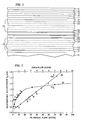
- FIG. 2 shows exemplary data on the precursor flow conditions necessary to grow InGaAsP layers that are lattice matched to InP, with ⁇ g ranging from 0.9 to 1.40»m.
- the data assumes that the flow of 70 sccm TMIn and 225 sccm of the 20% PH3 is kept constant at a rate that results in excess In and P in the growth atmosphere.
- Analogous remarks apply to compositions corresponding to points B, C, D, and E, as well as to all other points on the curves, as those skilled in the art will recognize.
- the quantity ⁇ g ⁇ g2 - ⁇ g1 exemplarily is divided into n parts that define the compositions at which the rate of change of TMGa flow and of AsH3 flow will be changed. Exemplarily, these correspond to points B, C, and D of FIG. 2.
- the TMGa and AsH3 flow rates corresponding to ⁇ g1 , ⁇ g2 , and to the 5 intermediate compositions at which the rate of change of the flow rates are to be altered are determined. Since the material growth rate at any given set of flow rates (at a given constant temperature) is known, the time required to grow any given sublayer can be readily determined. The sublayers will frequently be all the same thickness.
- the appropriate rate of change of TMGa flow rate is determined.
- the appropriate rate of change of AsH3 is determined. This procedure can be applied in analogous fashion to determine the appropriate rates of change of flow rates for all the other sublayers of the desired InGaAsP confinement layer.
- the flows of TMGa and AsH3 are changed, without growth interruption, such that the flows vary at the respective, previously determined new rates.
- the rate of change of the respective flows are again adjusted without interruption of the growth. This procedure is continued until all the sublayers are completed.
- the inventive procedure for growth of InGaAsP confinement layers requires only changes in the rate of change of gas flow, the growth of a confinement layer can be continuous, without cessation of growth upon completion of a given sublayer, as necessarily occurs in the growth of prior art step-wise graded InGaAsP confinement layers. This is considered to be a significant aspect of the invention, since defects tend to easily form from the ambient in the absence of growth.
- FIG. 3 shows exemplary data on the Ga content of a In x Ga 1-x As y P 1-y continuously graded confinement layer according to the invention, with y ⁇ 2.2x in the solid, and ⁇ g varying from 1.1»m at arrow 60 to 1.25»m at arrow 61.
- the Ga concentration varies continuously (linearly over a major portion of the layer thickness), thereby reducing the likelihood of defect formation.
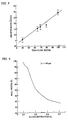
- FIG. 4 shows exemplary data on the In content of InGaAs as a function of TMIn flow rate. As can be seen, the dependence is linear, facilitating straightforward adjustment of the solid composition.
- Fig. 5 shows exemplary data on the growth rate of InGaAs as a function of TMIn flow rate (with TMGa and AsH3 flow fixed at 9 and 160sccm, respectively). The dependence is linear, with the growth rate under the exemplary conditions depending only on the TMIn flow rate.
- FIG. 6 shows an exemplary theoretical curve on the relationship between x (in In x Ga 1-x As) and the well width needed in order to obtain a lasing wavelength of 1.48»m.
- Experimental data we have obtained are in good agreement with the theoretical curve, at least for x ⁇ 0.43.
- x 0.53 the composition is lattice matched with InP.
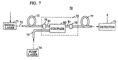
- FIG. 7 schematically depicts exemplary apparatus according to the invention, namely, optical fiber communication system 70.
- Signal laser 71 emits signal radiation 72 which is coupled into standard transmission fiber 73 and transmitted therethrough to fiber amplifier 76.
- Pump laser 74 emits pump radiation of an appropriate wavelength (e.g., 1.48»m) which is transmitted by means of a short length of fiber 75 into 76.
- the latter comprises a rare-earth doped fiber 81 coupled signal-transmissively, by means of conventional connectors 79, to 73 and to transmission fiber 77.
- the amplifier 76 also comprises means 80 to couple the pump radiation from 75 to 81. Such means can be conventional.
- Signal radiation is amplified in 76 in known manner, and is then transmitted through 77 to detector 78.
Landscapes
- Physics & Mathematics (AREA)
- Optics & Photonics (AREA)
- Condensed Matter Physics & Semiconductors (AREA)
- General Physics & Mathematics (AREA)
- Electromagnetism (AREA)
- Engineering & Computer Science (AREA)
- Nanotechnology (AREA)
- Chemical & Material Sciences (AREA)
- Biophysics (AREA)
- Crystallography & Structural Chemistry (AREA)
- Life Sciences & Earth Sciences (AREA)
- Semiconductor Lasers (AREA)
- Lasers (AREA)
Claims (10)
- Verfahren zur Herstellung eines Halbleiterlasers mit einer Emissionswellenlänge im Bereich von 1,2 bis 1,68 »m, der bei Raumtemperatur zu Daueremission fähig ist, wobei der Laser umfaßt:a) eine Einschlußschicht mit GaInAsP,b) einen aktiven Bereich mit einem oder mehreren Quantenmulden,
dadurch gekennzeichnet, daßc) die Ausbildung der Einschlußschicht das Aufwachsen einer Vielzahl von InGaAsP-Subschichten umfaßt, wobei sich die Zusammensetzung jeder Subschicht mit einer anderen Rate als Funktion des Abstands vom aktiven Bereich ändert, und
dadurch daßd) das Aufwachsen der Einschlußschicht kontinuierlich ist, ohne Wegfall des Aufwachsens bei der Vervollständigung einer gegebenen Subschicht, so daß die Zusammensetzung der Einschlußschicht sich kontinuierlich als Funktion des Abstands vom aktiven Bereich ändert, und Δa/a ≦ 3 x 10⁻⁴, wobei "a" die Gitterkonstante des Materials ist, an welche die Einschlußschicht gitterangepaßt ist, und Δa die Maximumabweichung von "a" der Gitterkonstanten im gitterangepaßten Abschnitt der Einschlußschicht ist. - Verfahren nach Anspruch 1,
ferner umfassend das Ausbilden des aktiven Bereichs derart, daß das Material wenigstens einer Quantenmulde verspannt ist. - Verfahren nach Anspruch 2,
bei welchem der aktive Bereich derart ausgebildet ist, daß der aktive Bereich wenigstens zwei Quantenmulden mit einer Barrierenschicht zwischen diesen umfaßt, wobei das Material der wenigstens zwei Quantenmulden verspannt ist, die Quantenschichtverspannung eine erste Richtung hat und in welcher ferner das Material der Barrierenschicht verspannt ist, wobei die Barrierenschichtverspannung in einer Richtung ist, die der ersten Richtung entgegengesetzt ist, wobei die gesamte Verspannung des aktiven Bereichs bei einem relativ niedrigen Niveau gehalten wird. - Verfahren nach Anspruch 1,
bei welchem der Laser derart ausgebildet wird, daß der Laser zu Daueremission bei Raumtemperatur mit wenigstens 50 mW optischer Leistung fähig ist. - Vorrichtung umfassend einen Halbleiterlaser mit einer Emissionswellenlänge im Bereich von 1,2 bis 1,68 »m der bei Raumtemperatur zu Daueremission fähig ist,
umfassend:a) eine Einschlußschicht mit GaInAsP,b) einen aktiven Bereich mit einer oder mehreren Quantenmulden,
dadurch gekennzeichnet, daßc) die Einschlußschicht eine Vielzahl von InGaAsP-Subschichten umfaßt, wobei sich die Zusammensetzung jeder Subschicht mit einer anderen Rate als Funktion des Abstands vom aktiven Bereich ändert und
dadurch daßd) die Zusammensetzung der Einschlußschicht sich kontinuierlich als eine Funktion des Abstands vom aktiven Bereich ändert und Δa/a ≦ 3 x 10⁻⁴ ist, wobei "a" die Gitterkonstante des Materials ist, an welches die Einschlußschicht gitterangepaßt ist, und Δa die Maximumabweichung von "a" der Gitterkonstanten im gitterangepaßten Abschnitt der Einschlußschicht ist. - Vorrichtung nach Anspruch 5,
bei welcher das Material von wenigstens einer der Quantenmulden verspannt ist. - Vorrichtung nach Anspruch 6,
bei welcher der aktive Bereich wenigstens zwei Quantenmulden mit einer Barrierenschicht zwischen diesen umfaßt, wobei das Material der wenigstens zwei Quantenmulden verspannt ist, die Quantenmuldenverspannung eine erste Richtung hat und wobei ferner das Material der Barrierenschicht verspannt ist, wobei die Barrierenschichtverspannung in einer der ersten Richtung entgegengesetzten Richtung ist, wobei die gesamte Verspannung des aktiven Bereichs bei einem relativ niedrigen Niveau gehalten ist. - Vorrichtung nach Anspruch 5,
bei welcher der Laser zu Daueremission bei Raumtemperatur mit wenigstens 50 mW optischer Leistung fähig ist. - Vorrichtung nach Anspruch 5,
bei welcher die Vorrichtung ein optisches Faserkommunikationssystem ist, welches umfaßt:i) einen Abschnitt einer mit Seltenen Erden dotierten optischen Faser,ii) eine Einrichtung zum Veranlassen des Flusses eines elektrischen Stroms durch den Laser derart, daß der Laser eine Ausgangsstrahlung aufweist, wobei die Ausgangsstrahlung eine Wellenlänge im Bereich von 1,2 bis 1,68 »m hat undiii) eine Einrichtung zum Koppeln wenigstens eines Teils der Ausgangsstrahlung in die mit Seltenen Erden dotierte optische Faser. - Vorrichtung nach Anspruch 6,
bei welcher die mit Seltenen Erden dotierte Faser Er umfaßt.
Applications Claiming Priority (2)
| Application Number | Priority Date | Filing Date | Title |
|---|---|---|---|
| US49214390A | 1990-03-13 | 1990-03-13 | |
| US492143 | 1990-03-13 |
Publications (3)
| Publication Number | Publication Date |
|---|---|
| EP0447096A2 EP0447096A2 (de) | 1991-09-18 |
| EP0447096A3 EP0447096A3 (en) | 1992-01-22 |
| EP0447096B1 true EP0447096B1 (de) | 1995-12-06 |
Family
ID=23955119
Family Applications (1)
| Application Number | Title | Priority Date | Filing Date |
|---|---|---|---|
| EP91301801A Expired - Lifetime EP0447096B1 (de) | 1990-03-13 | 1991-03-05 | Quantenstruktur-Laser mit einer InGaAsP-Begrenzungsschicht und Verfahren zur Herstellung des Lasers |
Country Status (3)
| Country | Link |
|---|---|
| EP (1) | EP0447096B1 (de) |
| JP (1) | JP2702819B2 (de) |
| DE (1) | DE69115086T2 (de) |
Families Citing this family (3)
| Publication number | Priority date | Publication date | Assignee | Title |
|---|---|---|---|---|
| JP2748877B2 (ja) * | 1995-01-13 | 1998-05-13 | 日本電気株式会社 | 半導体レーザとその製造方法 |
| DE59601142D1 (de) * | 1995-02-28 | 1999-02-25 | Siemens Ag | Integriert optischer wellenleiter mit einer einen steuerbaren komplexen brechungsindex aufweisenden wellenleitenden schicht |
| JP2877107B2 (ja) * | 1996-12-02 | 1999-03-31 | 日本電気株式会社 | 多重量子井戸型半導体レーザ |
Family Cites Families (4)
| Publication number | Priority date | Publication date | Assignee | Title |
|---|---|---|---|---|
| JPS59104189A (ja) * | 1982-12-07 | 1984-06-15 | Kokusai Denshin Denwa Co Ltd <Kdd> | 半導体レ−ザ |
| JPS6352792A (ja) * | 1986-08-21 | 1988-03-05 | Mitsubishi Electric Corp | レ−ザ加工装置 |
| JPS63161690A (ja) * | 1986-12-25 | 1988-07-05 | Nec Corp | 量子井戸型半導体レ−ザ |
| JP2898643B2 (ja) * | 1988-11-11 | 1999-06-02 | 古河電気工業株式会社 | 量子井戸半導体レーザ素子 |
-
1991
- 1991-03-05 EP EP91301801A patent/EP0447096B1/de not_active Expired - Lifetime
- 1991-03-05 DE DE69115086T patent/DE69115086T2/de not_active Expired - Lifetime
- 1991-03-12 JP JP3070393A patent/JP2702819B2/ja not_active Expired - Lifetime
Also Published As
| Publication number | Publication date |
|---|---|
| DE69115086D1 (de) | 1996-01-18 |
| DE69115086T2 (de) | 1996-08-08 |
| JP2702819B2 (ja) | 1998-01-26 |
| EP0447096A2 (de) | 1991-09-18 |
| EP0447096A3 (en) | 1992-01-22 |
| JPH06252512A (ja) | 1994-09-09 |
Similar Documents
| Publication | Publication Date | Title |
|---|---|---|
| US5040186A (en) | InP-based quantum-well laser | |
| Liau et al. | Low‐threshold InGaAs strained‐layer quantum‐well lasers (λ= 0.98 μm) with GaInP cladding layers and mass‐transported buried heterostructure | |
| JP3854693B2 (ja) | 半導体レーザの製造方法 | |
| Ha et al. | Long-wavelength GaInNAs (Sb) lasers on GaAs | |
| US5889805A (en) | Low-threshold high-efficiency laser diodes with aluminum-free active region | |
| US5289484A (en) | Laser diode | |
| JP3129779B2 (ja) | 半導体レーザ装置 | |
| Tsang | Heterostructure semiconductor lasers prepared by molecular beam epitaxy | |
| Kasukawa et al. | Very low threshold current density 1.3 μm InAsP/InP/InGaP/InP/GaInAsP strain-compensated multiple quantum well lasers | |
| Razeghi et al. | Recent advances in MOCVD growth of InxGa1-xAsyP1-y alloys | |
| US5175740A (en) | Semiconductor laser and method of fabricating same | |
| GB2353899A (en) | A quantum well semiconductor device with strained barrier layer | |
| Temkin et al. | High temperature operation of lattice matched and strained InGaAs-InP quantum well lasers | |
| US5914496A (en) | Radiation emitting semiconductor diode of buried hetero type having confinement region of limited Al content between active layer and at least one inp cladding layer, and method of manufacturing same | |
| EP0447096B1 (de) | Quantenstruktur-Laser mit einer InGaAsP-Begrenzungsschicht und Verfahren zur Herstellung des Lasers | |
| Valster et al. | Strain-overcompensated GaInP-AlGaInP quantum-well laser structures for improved reliability at high-output powers | |
| Bhat et al. | High-performance 1.3 μm AlGaInAs/InP strained quantum well lasers grown by organometallic chemical vapor deposition | |
| US20050230672A1 (en) | III-V compound semiconductor crystals | |
| EP0701309B1 (de) | Halbleiterlaserdiode | |
| Savolainen et al. | AlGaInAs/InP strained-layer quantum well lasers at 1.3 µm grown by solid source molecular beam epitaxy | |
| JPH0513884A (ja) | 半導体レーザ | |
| JPH0745909A (ja) | 歪量子井戸半導体レーザの気相成長方法 | |
| Tanbun-Ek et al. | Reproducible growth of narrow linewidth multiple quantum well graded index separate confinement distributed feedback (MQW-GRIN-SCH-DFB) lasers by MOVPE | |
| JP4944813B2 (ja) | 半導体光増幅器 | |
| JP2004165608A (ja) | 化合物半導体結晶及び化合物半導体デバイス |
Legal Events
| Date | Code | Title | Description |
|---|---|---|---|
| PUAI | Public reference made under article 153(3) epc to a published international application that has entered the european phase |
Free format text: ORIGINAL CODE: 0009012 |
|
| AK | Designated contracting states |
Kind code of ref document: A2 Designated state(s): DE FR GB |
|
| PUAL | Search report despatched |
Free format text: ORIGINAL CODE: 0009013 |
|
| AK | Designated contracting states |
Kind code of ref document: A3 Designated state(s): DE FR GB |
|
| 17P | Request for examination filed |
Effective date: 19920708 |
|
| 17Q | First examination report despatched |
Effective date: 19930519 |
|
| RAP3 | Party data changed (applicant data changed or rights of an application transferred) |
Owner name: AT&T CORP. |
|
| GRAA | (expected) grant |
Free format text: ORIGINAL CODE: 0009210 |
|
| AK | Designated contracting states |
Kind code of ref document: B1 Designated state(s): DE FR GB |
|
| REF | Corresponds to: |
Ref document number: 69115086 Country of ref document: DE Date of ref document: 19960118 |
|
| ET | Fr: translation filed | ||
| PLBE | No opposition filed within time limit |
Free format text: ORIGINAL CODE: 0009261 |
|
| STAA | Information on the status of an ep patent application or granted ep patent |
Free format text: STATUS: NO OPPOSITION FILED WITHIN TIME LIMIT |
|
| 26N | No opposition filed | ||
| REG | Reference to a national code |
Ref country code: GB Ref legal event code: IF02 |
|
| PGFP | Annual fee paid to national office [announced via postgrant information from national office to epo] |
Ref country code: FR Payment date: 20100402 Year of fee payment: 20 |
|
| PGFP | Annual fee paid to national office [announced via postgrant information from national office to epo] |
Ref country code: GB Payment date: 20100322 Year of fee payment: 20 |
|
| PGFP | Annual fee paid to national office [announced via postgrant information from national office to epo] |
Ref country code: DE Payment date: 20100419 Year of fee payment: 20 |
|
| REG | Reference to a national code |
Ref country code: DE Ref legal event code: R071 Ref document number: 69115086 Country of ref document: DE |
|
| REG | Reference to a national code |
Ref country code: GB Ref legal event code: PE20 Expiry date: 20110304 |
|
| PG25 | Lapsed in a contracting state [announced via postgrant information from national office to epo] |
Ref country code: GB Free format text: LAPSE BECAUSE OF EXPIRATION OF PROTECTION Effective date: 20110304 |
|
| PG25 | Lapsed in a contracting state [announced via postgrant information from national office to epo] |
Ref country code: DE Free format text: LAPSE BECAUSE OF EXPIRATION OF PROTECTION Effective date: 20110305 |