EP0446721B1 - Verteilter Verarbeitungsspeicher - Google Patents
Verteilter Verarbeitungsspeicher Download PDFInfo
- Publication number
- EP0446721B1 EP0446721B1 EP91103080A EP91103080A EP0446721B1 EP 0446721 B1 EP0446721 B1 EP 0446721B1 EP 91103080 A EP91103080 A EP 91103080A EP 91103080 A EP91103080 A EP 91103080A EP 0446721 B1 EP0446721 B1 EP 0446721B1
- Authority
- EP
- European Patent Office
- Prior art keywords
- memory
- data
- broadcast
- address
- chip
- Prior art date
- Legal status (The legal status is an assumption and is not a legal conclusion. Google has not performed a legal analysis and makes no representation as to the accuracy of the status listed.)
- Expired - Lifetime
Links
Images


Classifications
-
- G—PHYSICS
- G06—COMPUTING; CALCULATING OR COUNTING
- G06F—ELECTRIC DIGITAL DATA PROCESSING
- G06F9/00—Arrangements for program control, e.g. control units
- G06F9/06—Arrangements for program control, e.g. control units using stored programs, i.e. using an internal store of processing equipment to receive or retain programs
- G06F9/30—Arrangements for executing machine instructions, e.g. instruction decode
- G06F9/38—Concurrent instruction execution, e.g. pipeline, look ahead
- G06F9/3877—Concurrent instruction execution, e.g. pipeline, look ahead using a slave processor, e.g. coprocessor
- G06F9/3879—Concurrent instruction execution, e.g. pipeline, look ahead using a slave processor, e.g. coprocessor for non-native instruction execution, e.g. executing a command; for Java instruction set
-
- G—PHYSICS
- G06—COMPUTING; CALCULATING OR COUNTING
- G06F—ELECTRIC DIGITAL DATA PROCESSING
- G06F12/00—Accessing, addressing or allocating within memory systems or architectures
- G06F12/02—Addressing or allocation; Relocation
- G06F12/06—Addressing a physical block of locations, e.g. base addressing, module addressing, memory dedication
- G06F12/0646—Configuration or reconfiguration
-
- G—PHYSICS
- G06—COMPUTING; CALCULATING OR COUNTING
- G06F—ELECTRIC DIGITAL DATA PROCESSING
- G06F15/00—Digital computers in general; Data processing equipment in general
- G06F15/76—Architectures of general purpose stored program computers
- G06F15/78—Architectures of general purpose stored program computers comprising a single central processing unit
- G06F15/7807—System on chip, i.e. computer system on a single chip; System in package, i.e. computer system on one or more chips in a single package
- G06F15/7821—Tightly coupled to memory, e.g. computational memory, smart memory, processor in memory
Definitions
- the present invention relates generally to distributed processing and more particularly to integrated memory plus logic and systems for such integrated memory plus logic.
- a typical von Neumann computer system consists of a central processor unit (CPU) and a number of memory chips.
- CPU central processor unit
- memory chips The addition of multiple processors to increase processing power by parallel processing is a difficult task while the addition of memories for a single processor is relatively trivial. This is because processors need frequent access to the system bus and the presence of several in a system requires bus access arbitration.
- I/O input/output
- present parallel processing systems are termed bus or I/O limited which require expensive CPU-to-memory bandwidth and additional costly processors to increase system throughput.
- the ratio of computation to memory size can be continuously varied.
- a design may possess great computation capability as measured in millions of operations per second (MIPS) but all potential MIPS are not usable due to the cycles lost as the processors wait for data.
- MIPS operations per second
- the system performance is governed by the overall bandwidth of the system.
- the system bandwidth can be defined as the product of number of busses and the frequency of toggling.
- a system performance cost function can then be the electric power expended: Cost ⁇ Bandwidth ⁇ Capacitance ⁇ (VoltageSwing) 2 For a given system MIPS and system bandwidth, this cost function can be minimized by reducing the bus capacitance and/or the bus signal swing.
- WO 89 06014 A describes an integrated circuit memory chip for multiplication of a matrix and a vector.
- the matrix is loaded into a memory array and the vector is loaded into a buffer memory via a buffer data port.
- WO 88 01769 A describes a parallel data processing system which is formed as a binary tree of data processing elements.
- Each of the data processing elements includes a central processing unit and an interface unit having registers coupled to registers in the interface unit of adjacent higher and lower order elements in the binary tree. Signals comprising instructions and data for processing in the elements are broadcasted to the elements via the coupled registers for simultaneous processing in the elements. Processing results are compared and reported via the registers in a resolve/report operation.
- the present invention provides computer memory chips, as defined in claim 1, which include internal computational logic and secondary memory that may be broadcast to in all chips simultaneously and systems as defined in claim 5, with such memories.
- the memory chips may have a standard package pin configuration.
- the architecture allows easy expansion of the number of parallel Processing Elements by simply increasing the number of chips and permits massively parallel processing.
- the chips may also operate as conventional RAMs.
- a first order estimate of system throughput increase is given by the ratio of raw data to "information" data.
- information data.
- two bytes of information is the result obtained from 256 raw bytes.
- the system improvement is evident in that only two bytes of information are brought to the CPU rather than 256 raw numbers. That is, an improvement by a factor of 128.
- the number of MIPS and the throughput improvement may be orders of magnitude higher than the 128 of the previous example.
- the design of the chip allows easy expansion to provide the desired amount of distributed parallel processing power by simply increasing the number of chips.
- the preferred embodiment design also allows the system designer flexibility in setting processing power vs cost as the number of processing elements is defined by the memory chip count.
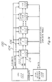
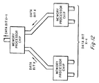
- FIG. 1a is a block diagram showing first preferred embodiment memories 110, 111, 112, ... 139 connected into a system 100 which includes a central processing unit (CPU) 102, 8-bit data bus 104, 11-bit address bus 106 (memories 110, 111, 112, ..., 139 each has a 2K by 8 SRAM section), 5-bit chip select decoder 108 for the thirty memory chips 110, 111, 112, ... 139, and the I/O 109.
- CPU 102 may be a simple processor such as a Motorola 6800 or Intel 8080 and has Write Enable and Ready pins connecting to each of the memories 110, 111, ... 139.
- System 100 is particularly adapted for computation intensive applications such as digital signal processing due to the structure of memories 110, 111,... 139 as described in the following paragraphs, although general purpose processing may be performed with each of the memories 110, 111, ... 139 acting as a 2K by 8 SRAM for a total of memory 60K by 8.
- Each memory 110, 111, 112, ... 139 is in fact a dual memory (data memory and broadcast memory) plus an embedded data path that includes application specific logic; see Figures 1b and 2.
- Embedding logic in the memory chip provides the on-chip advantages of low cost band-width and very fast memory access. Further, the inclusion of a broadcast memory in each chip allows the system to simultaneously use each chip's data path Processing Elements for massively parallel distributed computation. These memory chips share a standard pinout with a family of SRAM memories.
- each memory consists of three major circuit blocks:
- the chip floorplan strongly reflects the three components. From top to bottom, the Data Memory, the Application logic, and the Broadcast memory can be seen with clean demarcations of the Data Memory to logic and of the Logic to Broadcast Memory boundaries.
- the Data memory section contains all the addresses, chip select logic, and the V cc pads.
- the Broadcast Memory segment contains all I/O pads and V ss .
- This deliberate floorplan design methodology allows programmatic chip configuration to easily accommodate customized Application Logic sections of various sizes.
- the logic could be custom designed (gate arrays, standard cells, etc.), or configurable by the user by means of fuse or antifuse programming for specific applications.
- the logic can also be somewhat general, or even programmable logic with on-chip instruction decode to appear as a Harvard architecture.
- a higher density design could use a pinout similar to the standard 32K x 8 SRAM and the CPU could have 32-bit addresses.
- the first preferred embodiment also may utilize external signal pins for some of the logic that could be included in the chip.
- the conventional method of memory system Chip Select is shown in Figure 1a where the CPU provides five high order address bits to perform Chip Select decoding.
- the first preferred embodiment method of Chip Select also uses the five high order address bits decoding for Data Memory access but uses a register on each chip for access to the Broadcast Memory as follows.
- the programmable Broadcast Memory position in CPU address space is set using an Initialization register (the "CSB register") on each chip.
- Initialization of the CSB registers may be used to partition the system of chips into groups for response to Broadcast transmissions from the CPU. Initialization may be performed by the CPU at any time, allowing simple system reconfiguration. Initialization is performed on individual chips sequentially by writing to a series of two special addresses a number of times.
- This event is required to occur sequentially a number of times to eliminate the probability of random occurrence of writes to Data Memory appearing as Initialization.
- An event counter on each chip detects the sequence and then data on the data bus is written to the CSB register which defines the group for the chip.
- the clock for the event counter is supplied by an Address Transition Detection (ATD) circuit that pulses once for every address change. This is why the event is a series of two different addresses. Recall that the usual five high order address bit chip select singles out one chip at a time for this CSB register write during Initialization, but is inactive during broadcast instruction detection.
- All chips view the activity on the address bus, allowing its use for the broadcast of instructions.
- the design allows the simultaneous interrogation for instructions by all chips as the five high order address bit chip select is not requried to be active for instruction interrogation.
- the group identity is included in the broadcast instruction and only the chips in the requested group respond to the command.
- the instruction field is 11 bits for the 2K x 8 organization of the first preferred embodiment chips; the first three bits specify the command, one of the next five bits generate the ATD signal, and the last three bits define the group the chip belongs to by comparison with the stored value in the CSB register
- the following table shows a possible encoding with RRR a designation for the group: Instruction Address bits Begin Broadcast Write Mode 000 000001 RRR 000 00000 RRR Terminate Broadcast Write Mode 001 00001 RRR 001 00000 RRR Begin Local Computation 010 00001 RRR 010 00000 RRR Begin Self Test Mode 011 00001 RRR 011 00000 RRR Interrupt Local Computation 100 00001 RRR 100 00000 RRR
- a chip's event counter is incremented when the control logic senses a sequential occurrence of: the data on the address bus agrees with an instruction, the middle bits are as expected, and the requested group matches the group set in the CSB register.
- the event counter is satisifed when it reaches a statistically derived number of sequential events.
- the control logic circuitry then begins the requested operation for all chips in that group.
- CPU 102 would first Read an arbitrary chip's 000 00001 001 address, then Read address 000 00000 001 to provide an ATD generated clock pulse which causes the event counter to increment on all chips in group 001. A sequence of such Reads satisifies the event counter in each chip in group 001, which informs the on-chip control logic to perform the requested command 000 (Begin Broadcast Write Mode). In this instruction, the Broadcast memory chip select (CSB) for all chips in group 001 would become active. Then CPU 102 can execute a series of normal write cycles which will write to the Broadcast memory of each chip in group 001 simultaneously.
- CSB Broadcast memory chip select
- One chip may have both CSB and Chip Select for the Data Memory (CSD) active during Broadcast Write Mode, so the on-chip logic interprets this as a write to the chip's broadcast memory.
- CPU 102 completes the Broadcast Write task, it repeats the process but with the instruction now to Terminate Broadcast Write Mode by putting 001 00001 001 on the address bus. This informs the chips in group 001 to deactivate CSB and go into a normal mode.
- An alternative chip select scheme uses a combination of chip-level and board-level decoding to allow selection of one (or more) Broadcast Memories in a given CPU address space as follows.
- Each chip's Data Memory is mapped onto CPU 102's address space as in a conventional system. Specifically, CPU address 0-2K will be occupied by chip 110, addresses 2K-4K by chip 111, and so forth with addresses 58K-60K occupied by chip 139.
- the 2K interval of each Data Memory is defined by the 11-bit address bus 106.
- each chip may contain the inverters and the connection of true or complement may be performed by a register on-chip.
- CSB Broadcast Memory Chip Select location
- the true and complement of each of the five high order address bits are available on-chip with a set of five inverters. The values in the register determine whether the true or complement value is used to generate CSB, thus CSB is again a programmable entity.
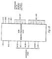
- FIG. 2 is a schematic block diagram of first preferred embodiment memory 110; memory 110 is fabricated as a silicon CMOS integrated circuit and packaged with the same pinout as a standard 16K SRAM organized as 2K by 8. This implies that a system with existing 16K memory chips could be converted to a system similar to system 100 by merely replacing the 16K memory chips with chips like memory 110.
- Memory 110 includes a 2K by 8 SRAM 202 (the Data RAM), a 256 by 8 SRAM 204 (the Broadcast RAM), Logic 206 (which includes the local Datapath with Application Logic Processing Elements), local 32-bit bus 208 between the Data RAM and the Datapath and local 32-bit bus 209 between the Broadcast RAM and the Datapath, 8-bit input/output port 210 which connects Data RAM 202 and also Broadcast RAM 204 to data bus 104, address multiplexer 212, Chip Select for Data Memory (CSD) input 214, Write Enable (WE) input 216, local address bus 218 which receives the 11-bit address from multiplexer 212, and Memory ready output or Output Enable (OE) input 220 (depending upon the CPU type).
- SRAM Data RAM
- 256 by 8 SRAM 204 the Broadcast RAM
- Logic 206 which includes the local Datapath with Application Logic Processing Elements
- local 32-bit bus 208 between the Data RAM and the Datapath and local 32-bit bus 209 between
- the external Ready pin is optional, although it is available for applications where standard pinout is not required.
- the Ready function will be performed by setting a reserved "flag" location in the Data RAM to a "not ready” value when local computation is begun in the memory.
- CPU 102 is only allowed to interrupt the local computation to poll the memory chips for the ready signal. Polling is done by a normal read. Interrupt is an instruction described infra .
- Broadcast RAM 204 is written to without the CSD signal present for memory 110; that is, all of the Broadcast RAMs of the memories 110, 111, ... 139 occupy the same address space of the CPU and may be written to simultaneously.
- the addresses of Broadcast RAM 204 occupy the upper eight bits of the eleven bit addresses.
- Data is written into or read from Data RAM 202 by CPU 102 by putting the address on address bus 106, activating CSD for memory 110, and activating WE.
- memory 110 operates in this mode as a standard 2K by 8 memory.
- FIG. 3 is a more detailed view of memory 110 illustrating some of circuitry.
- Memory 110 includes an array of 128 columns of 128 cells with a memory cell pitch of 15 x 20 ⁇ m.
- the Broadcast Memory is essentially a 128 x 16 section of the main array.
- the design is implemented in 1 ⁇ m CMOS technology.
- the ideal architecture would provide a 128 bit internal data path to maximize local data processing throughput.
- designing random logic in a SRAM cell pitch is quite difficult. Therefore, memory 110 uses a 4:1 multiplexing of the bit lines to sense amplifiers (and data path logic) and beefed up sense amplifiers to produce full logic levels internal to the chip.
- input/output port 210 in Figure 2 is merely illustrative of the connection of Data Bus 104 to the 32-bit internal bus.
- 4:1 bit line multiplexing allows considerable flexibility in the design of the Application logic needed to implement algorithms. For example, the space between adjacent columns is sufficient to to allow construction of multipliers and adders.
- the data path logic signals are at a 60 ⁇ m pitch which matches the non-extended gate array cell pitch. With respect to the Data Memory, the 4:1 multiplexing causes adjacent data (with respect to the data path) to appear in every fourth column. Thus, the data path signals are further organized in an ascending order so that any binary operation can pass "carry" signals, et cetera easily.
- memory 110 has a second mode of operation which includes local computation in the Datapath in Logic 206, and in this mode memory 110 appears as a slow memory to CPU 102.
- the Ready 220 output is low and when the local computation is complete Ready 220 goes high; the Ready outputs from memories 110, 111, ... 139 may be ANDed to CPU 102.
- no external Ready pin is employed to inform the CPU that local computation has completed.
- the CPU acts as a master to the slave memories at all times. The CPU polls the memories to determine if local computation has completed by reading a reserved location in each memory which holds the "ready flag" value.
- the CPU may perform Read operations by interrupting local computation by setting CSD low and proceeding as a usual read. If computation was interrupted, control logic 206 saves the state of the data path before proceeding with the CPU's read, then resumes when the CPU sets CSD high and WE low.
- CPU 102 writes the matrix elements T ij into the Data RAMs 204 of memories 110, 111, ... sequentially by first selecting the particular memory (for example, memory 110) with the CSD signal, putting an address (in the 2K by 8 RAM 202) on 11-bit address bus 106, the matrix element on 8-bit data bus 104, and putting WE high.
- the combination of low CSD plus high WE for memory 110 is interpreted by Logic 206 to have multiplexer 212 select the address from address bus 106 (and not from Logic 206) to put on local bus 218, and to have the row and column decoders of Data RAM 202 active, and to inactivate the row and column decoders of Broadcast RAM 204.
- the 8-bit matrix element on data bus 104 is written to the addressed 8 bits of Data RAM 202. This is repeated until Data RAM 202 has all of the required matrix elements written in.
- the unselected memories (111, 112, ... ) have a high CSD but their Logic units do not interpret the high going WE as writing to the Broadcast RAMs because the alternating addresses to satisfy the event counter do not occur, so nothing is written to either the Data RAMs or the Broadcsat RAMs.
- CPU 102 After CPU 102 has written matrix elements into Data RAM 202 of memory 110, it writes matrix elements into the Data RAM of memory 111, and so forth until the matrix is loaded into the Data RAMs of the memories 110, 111, 112, ...
- CPU 102 writes the vector components V j plus a local compute instruction into all of the Broadcast RAMs of memories 110, 111, .... simultaneously by first alternating the two addresses used to satisfy each chip's event counter and inform the on-chip Logic to activate the Broadcast Memory Chip Select (CSB) for write cycles to the Broadcast RAM. Note that there is no grouping of chips with the CSB registers for this computation. CPU 102 then makes normal writes that are simultaneously into all of the Broadcast RAMs.
- Logic 206 sets multiplexer 212 to pass the address from address bus 106, deactivates the decoders for Data RAM 202, and activates the decoders for Broadcast RAM 204 to write the vector components plus local compute instruction into Broadcast RAM 204.
- the alternating addresses method is used to terminate the Broadcast Memory write as previously described.
- the CPU may first store instruction information in the Broadcast RAMs which the control Logic 206 uses to determine the size of the matrix block that has been allocated to each memory and thereby set address loop counts for the required internal read operations.
- the control Logic 206 could be viewed exactly as the control logic of a conventional microprocessor.
- the application specific data path can be designed to perform complex function limited only by chip area and the desire to fit into a standard pinout package.
- Logic 206 When CPU 102 sets WE low, and with CSD high to all chips 100, 111, ... the Logic 206 of each memory initiates the local computation sequence. Logic 206 first generates the address(es) for the location in Broadcast RAM 204 that would contain any local compute instruction and set multiplexer 212 to pass this address, sets the Ready flag (or pin) to not ready, plus deactives the decoders for Data RAM 202 and activates the decoders of Broadcast RAM 204 and reads the contents of the address(es). If the address(es) contain the local compute instruction, then Logic 206 for each memory simultaneously goes into the following loop:
- Step (i) to (ix) are repeated n times with the remaining rows of matrix elements in Data RAM 202 but the same vector components V j from Broadcast RAM 204 to form and store the components W k +1 , W k +2 , ..., W k + n .
- V has 100 components
- 7 rows of Broadcast RAM 204 are needed to store the components, and the seventh row will only be 4 / 16 used.
- the loop terminates after all of the rows of Data RAM 202 used to store the block of matrix rows have been gone through. Simultaneously memories 111, 112, ... are computing and storing all of the other components W 1 , W 2 , ... W M . Logic 206 then sets the Ready flag (or pin 220) high, and CPU 102 may read the result from Data RAM 202 by putting CSD low while retaining WE low so Logic 206 will have multiplexer 212 pass the addresses on bus 106 and activate the decoders for Data RAM 202. This local computation avoids the fetching of each of the matrix elements by CPU 102 for computation and thus avoids much traffic on busses 104 and 106. Indeed, during the local computations by memories 110, 111, ..., CPU 102 may be involved in other tasks.
- a second example of local computation again describes matrix multiplication by a vector.
- Matrix T ij is 252 x 252.
- Vector V j has 252 elements.
- the result will be the 252 element Vector W j .
- each element is 8 bits wide.
- the 2K x 8 Data RAM cannot hold the full matrix T ij so T is broken into 32 blocks of 8 rows with 252 elements in each row. Each block occupies 16,128 bits which is 126 columns of the 128 x 128 bit Data RAM. The remaining 4 bytes of the Data RAM are to be used to store the result.
- the required number of memory chips is 32.
- the program begins by writing the 32 blocks of matrix T ij into all 32 Data RAMs sequentially as usual (as described in the previous example).
- Vector V j is then written into all Broadcast RAMs concurrently.
- the Broadcast RAM is 256 bytes (16 rows by 128 columns) so Vector V j occupies 252 bytes (16 rows by 252 columns).
- the operations are all 32 bit wide and control of computation is greatly eased by aligning the computation to this width. This is accomplished by setting up matrix block segmentation rules for the system. Our 252 element examples avoid this step for pedagogical simplification.
- the required data path circuitry in Logic 206 includes four 8-bit Booth multipliers and an adder to sum the products.
- An alternate data path configuration would include a single 8-bit multiplier and an adder. This would also require registers for the operands and a multiplexer to select one of the four sets of operands. Clearly, this reduces the number of parallel Processing Elements (PEs) but would reduce data path silicon area.
- PEs parallel Processing Elements
- the local computation is then initiated in all 32 chips which sets the Ready flag to not ready.
- the CPU is now free to perform other tasks.
- the sequence of computation would present the first four elements (32 bits) of matrix T ij from the Data RAM and the first 4 elements of Vector V j from the Broadcast RAM to the data path logic circuitry.
- the multiply and add are done, the next four corresponding elements of both T ij and V j are presented from the Data and Broadcast RAMs, respectively, until all 252 elements in the first row of matrix T ij are operated on.
- the single 16-bit result element for that row is then stored in the available Data RAM space. This routine is repeated until all 8 rows of the block are operated on.
- the Ready signal is set in all chips and the CPU may read the eight 8-bit result elements from each of the 32 chips.
- the total operation time is:
- the memory load is a constant 63,756 cycles. Assume the very best case for the conventional system so that calculation and read operations are pipelined in the CPU and that there are no lost cycles missing data during reads. Assume that the CPU employs the same Booth multiplier/accumulator circuitry so that the number of clock cycles per operation is the same as in the preferred embodiment data path.
- the CPU must have 252 ⁇ 252 + 252 board level reads for the matrix and the vector elements for an additional 63,756 cycles. Assuming perfect pipelining of reads and computation, we have 4 cycles required for each of the 252 ⁇ 252 ( n 2 ) computations for a total of 259,016 cycles. The total operation then requires 317,772 cycles for a conventional system if memory load time is included and 254,016 cycles if it is not.
- the performance improvement is thus a factor of four if memory load is considered. If we assume that memory load is a given, we see that the preferred embodiment system provides a factor of 69 improvement in speed.
- the preferred embodiment system reduced the CPU to memory board-level I/O by a factor of 63,756/252 ⁇ 253 by reducing the raw data to information before sending it to the CPU. If one considers the additional multiplicative factor of the ratio of board-level bus capacitance to chip-level bus capacitance, it is clear that system power requirements have been significantly reduced.
- Matrix T ij is 252 x 252.
- Matrix U ij also has 252 x 252 elements. The operation is exactly the same as multiplication by a vector, we now simply treat each column of matrix U ij as we did the vector V j .
- Matrix T ij is again segmented into blocks; the first 31 memories again receive eight rows and the 32nd memory gets the last four rows. Thus, the memory load of matrix T ij again requires 63,504 cycles.
- Matrix U ij is broadcast a segment at a time to all Broadcast RAMs.
- the preferred embodiment system provides a factor of 91 improvement. Including all memory load cycles, the improvement provided by the system is a factor of 84.
- a fourth example of local computation is a sparse matrix operating on a vector.
- the Data Memory of each chip is filled with elements of the sparse matrix. Presume that 64 bit words are used for the matrix elements and that 16 bit words can be used for the row tag and column tag for the matrix element; also 64 bit words for partial inner product results. Thus, three 32 bit words hold the tags and the matrix element.
- the datapath 206 will contain a 64 bit multiplier and accumulator plus logic to test if the current word has a counterpart in the Broadcast Memory to by multiplied against. Again, the vector to be operated on is broadcast to all chips simultaneously and the control logic 206 sequences through the Data Memory as in the first example.
- the Data Memory is filled by CPU 102 with tagged words of the sparse matrix in any order, but grouping words from the same matrix row into the same chip's Data Memory reduces result data that need to be read by CPU 102.
- the matrix elements are cycled through as previously described and the tags are tested to see if the word is to be mulitplied, and, if it is, where to store the result.
- the tags are tested to see if the word is to be mulitplied, and, if it is, where to store the result.
- not all of the vector may fit in the Broadcast Memory and it will need to be broadcast in pieces as in the case of the nonsparse matrix multiplication example.
- Each time a piece of the vector is broadcast each chip must cycle through all of the matrix elements to see which words are to be multiplied; this need to cycle through all of the matrix elements makes the number of multiplications per second smaller than in the nonsparse case, which only has to cycle through the portion of the data memory corresponding with the piece of the vector which has been broadcast.
- the inner products are stored in the Data Memory, the number of locations that need to be reserved for them is equal to the number of different rows that are on the chip.
- CPU 102 can read the resultant vector. It needs to go to each chip sequentially, reading inner products for the rows that are stored in the DAta Memory.
- the system performance for a sparse matrix acting on a vector can be estimated as follows. Assume each memory has 16K Data Memory with 2K Broadcast Memory, 20 nsec internal cycle time, 40 nsec external cycle time, with a PLD to buffer and arrange data from CPU 102, and a pipelined datapath read/multiply/accumulate. Then for a 256 by 256 sparse matrix with an average of 10 nonzero elements per row, each Data Memory will hold about 18 rows of the matrix: 10 64-bit words per matrix row plus one 64-bit word for the inner product of the row with the vector plus row and column tags (16 bits each) for each of these 11 64-bit words per row implies a total of 33 32-bit words per matrix row. Thus a 16K Data Memory will hold 15 matrix rows, and about 18 chips are needed to hold the entire matrix. The Broadcast Memory holds one eighth of the vector.
- Another example illustrates implementation of a neural network algorithm described in U.S.Pat.No. 4,326,259 with the system 100.
- a neural network algorithm described in U.S.Pat.No. 4,326,259 with the system 100.
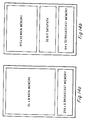
- 1,000 internal nodes each connect to all inputs (responding to some and not to others according to a vector W); each internal node has a settable threshold ⁇ ; 50 output nodes potentially connected to any or all of the input nodes and each output node with threshold 1; and 50 outputs, one for each output node (see Figure 15);
- the Data Memory is 1,000 words, each 128 bits wide. The number of words is equal to the number of internal nodes.
- the 128 bits in each word store four things: the first 100 bits is a vector representing the input vector W that the input responds to, the next 8 bits store the threshold ⁇ , the next six bits indentify the one output node (part of the alogrithm) that this internal node outputs to, and the next bit indicates if this internal node is committed (part of the alogrithm); see Figure 16.
- a final word in the Data Memory is used to store the 50 bit output vector of the chip.
- the datapath consist of a 100 bit Hamming distance calculator, comparator to compare the resulting Hamming distance with the requried threshold, plus additional control logic specific to the alogrithm and the learning phase of the algorithm, together with the ususal control logic to sequence thorugh the Data Memory and detect instructions.
- the Broadcast Memory stores the 100 bit input vector to the chip known as the input layer in the algorithm.
- the chip In normal operation (not during training) the chip operates as follows.
- the ouptut vector is set to all zeros, the input vector is written into the Broadcast Memory, and the chip cylces through the 1,000 128-bit Data Memory locations to calculate the output vector, and the CPU reads the location containing the output vector.
- the j th 128-bit Data Memory location is read, if the vector is committed (115th bit), then the Hamming distance between the first 100 bits representing W j and the input vector is calculated and compared with the 8-bit threshold ⁇ j of this internal node. If the Hamming distance is greater than the threshold, then the bit in the output vector identified by the next six bits of the 128-bit location is set.
- the time for the chip to operate in normal mode is the time for the chip to cycle through all of the internal nodes.
- For learning mode, committing internal and output nodes is the time for a memory write, switching off internal nodes for a particular input is two times normal mode as each access must not only calculate the Hamming distance but write back the new threshold.
- a Built-In Self-Test (BIST) and Automatic Fault Tolerance Scheme suitable for smart RAMs such as memories 110 can be achieved by adding a third mode of operation to memories 110 that causes a self-test mode to run as indicated in the chip select discussion, supra .
- CPU 102 writes a Begin Self-Test Mode command and the datapath control logic then initializes the memories to designer-determined values, cycles that the data of all addresses, and compares the results with the designer determined expected result value. Fails are flagged in special RAM locations.
- Tests of the datapath control logic may also be included; indeed for memories adapted to matrix multiplication the test of the datapath could be simply a mulitplication of all zero matrices so a result other than zero would set a fail flag.
- All chips perform BIST in parallel. When complete, the CPU then polls (performs a read of a fail flag) each chip and notes the addresses of failed chips, and switches them out in address space with a redundant chip supplied on the board. Typically, BIST would be performed prior to loading data in the Data RAMs.
- Figure 4 is a schematic block diagram of a second preferred embodiment memory 400 that includes local computation circuitry but with standard memory package pinout.
- Memory 400 is configured for search through a linked list of vectors in RAM 402. Each vector would have one or more fields and a pointer to the next vector in the list; and a search through the list would typically include the following steps:
- LOADAC load accumulator
- STOREAC store accumulator
- ADD add to accumulator
- SUB subtract from accumulator
- BRANCH ⁇ 0, BRANCH > 0, BRANCH 0, BRANCH ⁇ 0, BRANCH ⁇ 0, BRANCH ⁇ 0 (six accumulator test conditions), IDLE, and MAX (put in accumulator
- l 1 and l 2 norms of vectors may also be performed with memories 110, 111, 112, ... such as computation of l 1 and l 2 norms of vectors.
- digital signal processing often requires the finding the "distance" between a test vector, , and each of a number of reference vectors, W ⁇ for 1 ⁇ ⁇ ⁇ R, and the commonly used measurements of distance are the l 1 and l 2 norms of the differences, - W r .
- the l 1 norm of the difference is and may be computed by loading the components W r / j into Data RAM 202 and the components j into the Broadcast RAM 204 as previously described and then doing the subtraction and absolute valuing in parallel in Logic 206 for each reference vector.
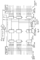
- Figure 5a is a schematic block diagram of a third preferred embodiment memory 500 that includes local computation circuitry but with standard memory package pinout analogous to first preferred embodiment memory 110.
- Memory 500 is especially adapted for a multiply and accumulate computation as occurs in the calculation of l 1 and l 2 norms of vectors and vector dot products.
- Memory 500 includes 256K Data RAM 502 which is organized as 32K x 8 bits (512 by 512 array of memory cells which are multiplexed 16-to-1 to bus 508), 32K Broadcast RAM 504 which is organized as 4K x 8 bits (64 by 512 array), 32-bit Data bus 508, 15-bit Address bus 506, a multiply-accumulate pipeline (16-bit by 16-bit multiplier 510, 32-bit multiplexer 512, 32-bit shifter 514, 32-bit multiplexer 516, 32-bit ALU 518 which has one entry feedback, 32-bit accumulator 520, and 32-bit shifter 522), 32-bit registers 524 and 526 that hold data just read in from the RAMs and unpack it in that 1, 2, 3 or 4 bytes of the contents are accessible as illustrated, Address registers 528-530 which auto-increment or auto-decrement with register 524 or 526 unloading, and ten control words 532 that can be programmed by the external CPU.
- 32K Data RAM 502
- unpacking registers 524 and 526 The function of unpacking registers 524 and 526 is to allow the selection of the data bit width to be 1, 2, 3, or 4 bytes (8 bits equal 1 byte) even though the data bus is of fixed width (32-bits in this embodiment).
- An examplary implementation of unpacking register 524 could be four 8-bit registers which are written in parallel by Data bus 508.
- the "Data Width" control word generates four control signals which are then logically combined with a clock signal to control four banks of pass gates which place the desired data to multiplexer 512 inputs. See Figure 5b for a simple schematic.
- Unpacking registers 524 and 526 also allow pipelined data loading to multiplexer 512 without additional memory reads by shifting the data words as needed.
- Memory 500 is typically part of a system with a CPU and multiple memories similar to memory 500.
- the external data bus and multiplexer analogous to bus 104 and port 210 of Figure 2 are not shown in Figure 5a, and the external address bus is multiplexed with Address registers 528-530 as suggested in Figure 5 and analogous to multiplexer 212 of Figure 2.
- Alternative arrangements include replacing the 16-to-1 multiplexing of the 512 bitlines of Data RAM 502 to 32-bit bus 508 with four 4-to-1 multiplexings of the 512 bitlines to four 32-bit busses and have four multiply-accumulate pipelines and pairs of 32-bit unpacking registers. Further, the 16-bit by 16-bit multiplier 510 could be replaced with a 24-bit by 24-bit or even a 32-bit by 32-bit multiplier.
- the first three of the ten control words 532 specify the start-address of a matrix, the number of rows, and the number of columns in a matrix.
- the fourth and fifth control words specify the width of the data; the sixth control word specifies the address at which the computed results are to be stored the seventh control word sets up the shifter, the eighth control word sets up the configuration (multiplexers 512 and 516, autoincrement or decrement, and so forth), the ninth control word is the GO word which when written to begins computation in the memory 500, and the tenth control word specifies the start address of the vector in Broadcast RAM 504.
- memory 500 may be part of a system which has reference data loaded into Data RAM 502 and input data simultaneously written to all Broadcast RAMS 504.
- An exemplary application would be real time speech recognition which computes Euclidean distance of an input vector from stored reference frames.
- the reference frames are distributed equally amongst the memories in Data RAM and as the input vector comes in it is simultaneously written to the Broadcast RAMs and the GO word written to initiate simultaneous computation in each chip. Upon completion of the local computations the GO word is changed by the memory and the external CPU may read the results.
- X [ x (1), x (2), x (3), x (4)]
- R (1) [ r (11), r (12), r (13), r (14)]
- n 8
- d ( n ) is a scalar requiring two bytes of storage.
- the r ( i , j ) are stored in data RAM 502.
- x ( i ) and r ( i ) are one byte wide each. The following sequence of steps discuss how the computation is done.
- Another example would be the difference-magnitude-accumulate between X and R .
- the control word OPERATION would flag this difference-magnitude-operation to be performed.
- the execution of this computation would be similar to the one just described; the difference would only be in step 5 where the OPERATION control word would cause the logic to take th edifference betrween x ( i ) and r ( j , i ), and the absolute of this would be accumulated.
- FIG. 5c shows memory chip 568 with the lower part 570 of the memory regarded as program memory and the upper part 572 as data memory.
- Program memory 570 is accessible from the external world (CPU) using the same I/O pins as data memory 572 as previously described.
- the on-chip decoder 574, memory-controller 576, and logic 578 provide the programmable processor. Instruction are fetched from program memory 570, decoded in decoder 574 which generates appropriate control signals to operate logic 578.
- memory-controller 576 puts logic 578 on hold; and when the external world access is completed, memory-controller 576 releases logic 578 which resumes execution.
- a fourth preferred embodiment memory and system may be used as an address-associative memory (also called a Sparse Distributed Memory or a Kanerva Memory).
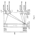
- Figure 6 is a schematic block diagram of a fourth preferred memory system, generally denoted 600, which includes address memories 610, 611, 612, ... and data memories 650, 651, 652, ....
- Figure 7 is a schematic block diagram of fourth preferred embodiment memory 610 that includes Address RAM 702 (which corresponds to the Data RAM 202 of memory 110), Broadcast RAM 704, and Logic 706. Memory 610 together with other similar memories 611, 612, ... form an address-associative memory system 600.
- An address-associative memory differs from a usual memory by permitting data stored at one address to be retrieved by reading a close-by address; thus a sort of fault tolerance is inherent.
- an address-associative memory with a input address and a piece of input data could write the data to all memory locations with an address within a certain Hamming distance from the input address and the written data would not displace data already at any of these locations but would be added to it (each bit of the memory is effectively replaced by an up-down counter).
- An input address for reading data would activate all addresses within a certain Hamming distance from the input address and a bitwise thresholded sum of the data at all of these activated addresses creates the output data read.
- addresses are 32 bits long (so there are about 4.3 x 10 9 possible addresses) and if 10,000 32-bit words, A 1 , A 2 , ... A 10 , 000 , are randomly selected to be the key addresses, then the Hamming distance between A 1 and the closest other key address is expected to be roughly 4 and the Hamming distance between A 1 and the hundredth closest other key address is expected to be roughly 8-10.
- the loading of data into system 600 proceeds as follows: first the 10,000 key addresses are generated (random number generator) and stored in the Address RAMs of the memories 610, 611, ... , each Address RAM has room for 512 addresses, so memories 610, 611, ... 629 provide sufficient space.
- CPU 602 also creates a lookup table correlating each key address with an address in Data memory 650, and in Data Memory 650 each data word occupies 256 bits organized as 32 by 8; thus Data Memory 650 must have at least 25.6 megabits.
- 32-bit data is stored at an input address (or even to a random input 32-bit address) by intially finding the 250 or so key addresses of the 10,000 that are within a Hamming distance of 10 of the input address.
- CPU 602 writes the 32-bit data to each of the locations in Data Memory 650 that correspond to the found active addresses. These writes of the 32-bit data do not replace any data already stored at the data words, but rather is added to it: this is accomplished by using the 8 bits in the 32 by 8 organization of the data words.
- the 8 bits act as an up-down counter of range 128, and each bit of the 32-bit data word either increments (if the bit is a "1") or decrements (if the bit is a "0") the counter.
- Data memory 650 could have 32 parallel adders for this computation if the storage of data represents significant overhead time.
- data may be read by writing an input address to the Broadcast RAMs, locally finding all 100 or so active addresses within a Hamming distance of 10 of the input address, reading the 100 or so corresponding data words from Data memory 650, averaging the 8-bit up-down counters over these 100 or so data words on a counter-by-counter basis, and thresholding to convert the averages to a 32-bit binary output.
- the fifth preferred embodiment is another address-associative memory system but with different memory organization.
- Figure 8 is a schematic block diagram of a fifth preferred embodiment memory 800.
- Memory 800 includes RAM 802 which would contain both the key addresses and their data together with an accumulator in Logic 806 for the data write to the key addresses.
- Memory 800 has the same pinout as a standard 2K by 8 SRAM and includes RAM 802 which is also organized as 2K by 8 and appears to the CPU as a 2K by 8.
- RAM 802 can contain six 256-bit key addresses plus associated 256-item data with each data item being 8 bits to act as an up-down counter of range 128. This leaves a little more than 2K bits in RAM 802 for storing results and which may be read later by CPU.
- the CPU can write a key address to thirty-two successive 8-bit bytes and the associated data to the next 256 successive bytes in RAM 802.
- memories 800 do not require a lookup table to correlate a key address with its stored data. Instead, given an input address, CPU simultaneously writes the input address (as thirty-two bytes) to the Broadcast RAM 804 of each memory 800 in the system together with a local search instruction.
- Logic 806 then reads the local search instruction, sets the Ready signal low, and begins a computation of the Hamming distance between the input address and each of the six key addresses stored in RAM 802.
- Logic 806 interrupts its cycling through the active addresses and reads the data associated with the found active address and adds it to the accumulators 812, and may store the results in the approximately 2K of RAM 802 unused for key address-data. After the all of the six key addresses have been compared to the input address and all corresponding data, if any, is summed and stored in RAM 802, the Ready signal is set high. CPU can then read the results of each memory 800 and sum and threshold to recover the data read.
- To write data to memory 800 is more involved than reading because the data must be added to the preexisting data at each key address close to the input address.
- Either CPU can read the stored data for each key address found within a Hamming distance of 10 of the input address and add the new data and restore, or the data can be simply sent with the input address to the Broadcast RAM 804 and Logic 806 can do the additions in accumulators 812.
- a sixth preferred embodiment system uses many memories such as memory 800 in a sparse distributed memory (SDM) machine 900 and schematically illustrated in Figures 10a-c.
- the building block for the SDM machine is a memory/processor chip containing 16K bits of memory and 32 bits of custom datapath.
- the memory of each chip is used to store six, 256 bits wide, SDM addresss-data pairs ( Figure 10a).
- the datapath of each chip controls and executes the SDM read and write operations, and has special logic to compute hamming distance and do SDM style accumulations ( Figure 10a).
- the SDM machine consists of one or two boards (depending on required capacity) predominantly populated by 512 of the memory/processor chips ( Figure 10b).
- the boards plug, for the purpose of this embodiment, into a TI Explorer Lisp machine ( Figure 10c). They appear to the Lisp CPU as memory boards.
- the Lisp CPU interfaces with them by writing the Sparse Distributed Memory (SDM) address (and data on a write) to predetermined memory locations and the memory/processor chips do the SDM computation.
- SDM Sparse Distributed Memory
- the processor waits ( ⁇ 100 ⁇ sec) and then reads the SDM (non thresholded) data from predetermined memory locations from each board in sequence.
- the Lisp CPU accumulates the data from each board and thresholds the result.
- Each board holds 512 memory/processor chips, and can store 3072 SDM locations, each location being 256 bits long, using 8 bit data counters.
- the CPU can access the SDM for a read or write 10,000 times per second as follows:
- the boards appear to the Lisp CPU as memory boards they are easy to add to the system. In the case of the TI Explorer, they will be plugged in to the Nubus backplane, and used as memory boards. To use them to do the SDM computation the Explorer system must be inhibited from using the boards as paging space. The software to do the SPM read or write will write to predetermined memory locations on the board that are decoded by special board hardware to activate the memory/processor chips for the SDM compuation.
- Each memory/processor chip consists of a 16K memory seen internally as a 512 x 32, a 2K broadcast memory seen internally as a 64 x 32, and a datapath that has full 32 bit access to both memories.
- the memory is logically divided into six address data pairs and a region in which to accumulate the data on a read.
- Figure 9 shows the logical structure of the memories.
- the 16K memory is used to store the SDM address and data
- the broadcast memory is used to store the data needed for each SDM read or write
- the datapath does the SDM computation.
- the datapath has special logic to compute the hamming distance of a 32 bit word in one clock cycle, and four SDM style accumulators to operate, in parallel, on the four data "bits" that are stored in each word.
- the datapath is heavily pipelined for maximum speed.
- the datapath Upon receiving the broadcast of the read or write information, the datapath proceeds to cycle through each of the SDM addresses, one word at a time, calculating the Hamming distance to the target SDM address that it is cycling out of the broadcast memory, and accumulating the partial Hamming distance into a total Hamming distance.
- the total Hamming distance is compared with the threshold to determine if the address is active. If not active, the datapath goes onto the next SDM address, if active, the data update - on a write, or data accumulate - on a read happen. On data update, the SDM "bits" are incremented on write of a 1, and decremented on write of a 0. On a data accumulate, the data is read from the main memory the result so far is read from the main memory, and their addition is written back into the main memory.
- the datapath and accumulation region are also used in the hierarchical boardwise data accumulation on an SDM read that is described below, where data for bit x - 1 is cycled in through the hierarchy input pins and accumulated, whilst data for bit x is cycled out of hierarchy out pins.
- Each board consists of 512 memory/processor chips, each chip contains six, 256 bit wide SDM addresses and associated data. Also on each board are off the shelf parts to do the Nubus access, signal driving, and predetermined memory location detection.
- the 512 memory/processor chips are orgainzed in three ways, as:
- the regular memory supports non-SDM use, and SDM initialization
- the binary tree supports boardwise accumulation of data during SDM read
- the broadcast memory (all chips getting memory writes simultaneously) supports writing of the SDM addresses, data, and threshold.
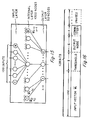
- SDM read or write On a SDM read or write, address and data are written to a predetermined memory location. Special logic detects this and enables all memory/processor chips for write. The SDM address and data and threshold and read/write flag are then written to all memory/processor chips. On a SDM read each chip does data updates locally, no interchip communication is required, this can be accomplished in 3.6 ⁇ sec. On SDM read each chip accumulates data from its active SDM locations locally, then a boardwise accumulation of the data that has been accumulated in each of the 512 chips takes place. The chips are connected in a hierarchy to facilitate this operation. The hierarchy is 8 deep and branching factor 2, with the extra 512th chip added specially in at the top ( Figure 11).
- the hierarchy enables all the level 8 chips can be passing data to their level 7 parents together.
- Six extra pins on each memory/processor memory chip are provided for the hierarchical connection: two up (HO0 and HO1), and four down (HL0 and HL1 for left child and HR0 and HR1 for right child).
- the passage of data up the hierarchy is also pipelined 8 deep: whilst byte x is passing from level 2 to level 1, byte x + 1 can be passing from level 3 to level 2 and so on. With these features the data transmission for the whole board takes 84 ⁇ sec.
- off-the-shelf logic is used to buffer the data into 64 32-bit words.
- This buffer logic has 32-bit output to the Nubus backplane. With the data 32 bits wide, and buffered, full use of the Nubus burst transfer mechanism can be used to transmit the SDM read data to the CPU in 6.8 ⁇ sec.
- the memory/processor chips also have 23 pins to allow them to be connected as a 2K x 8 memory ( Figure 13). Using these connections the 512 memory/processor chips are connected in a regular memory structure and the board appears to the CPU as a 256K x 32bit memory board.
- the regular memory structure facilitates the initial writing of the SDM addresses, allows the board to be used as a regular memory board, and gives observability and controlabiliy for system test and debug.
- the final chip/board architectural feature is the broadcast mode.
- Each chip has an additional 2K x 8 broadcast memory that is used to receive data that will be broadcast to all chips at once. Off the-shelf-parts are used to detect a memory write to a special location. When this happens the broadcast mode pin on each memory/processor chip goes high. This selects all chips, and memory writes can happen into the 2K x 8 broadcast memories.
- the SDM address, data and active radius and read/write flag are broadcast to each chip.
- Figure 14 shows the block structure of the memory/processor chips.
- the SDM machine has the following good architectural features:
- Speech recognition dynamic time warping and hidden markov model approaches
- matrix multiplication are applications that map well to this architecture.
- This system design can be grown in a number of ways
- the SDM machine should solve the application proposed here on a single board.
- the main features of the machine are its speed, its ease of use, and the possibilities for much larger SDM machines of the same architecture.
- the dimensions and shapes and sizes of the RAMs, logic, busses, and so forth could be varied.
- the Data RAM could be ROM or PROM for applications where the data is always the same; or the Data RAM could be EPROM or EEPROM for infrequently changing data. This would allow the system to be nonvolatile.
- a load-store processor could be integrated into the smart memories with the Broadcast RAM regarded as the program memory and the Data RAM as the data memory so a Harvard architecture results. Further, computation or data-intensive kernels would be downloaded to the program memory.
Claims (10)
- Als integrierte Schaltung ausgeführter Speicherchip (110, 210, 400, 500, 610) auf dem Logik eingebettet ist, mit:einem Datenspeicher (202, 402, 502, 702, 802), wobei der Datenspeicher (202, 402, 502, 702, 802) direkt über einen Ein-/Ausgangsmultiplexer mit einem Datenbusanschluß gekoppelt ist,einem Chipauswahlanschluß (214), der mit dem Datenspeicher (202, 402, 502, 702, 802) gekoppelt ist,einem Broadcast-Speicher (204, 404, 504, 704, 804), wobei der Broadcast-Speicher (204, 404, 504, 704, 804) direkt über den Ein-/Ausgangsmultiplexer mit dem Datenbusanschluß gekoppelt ist und wobei der Broadcast-Speicher (204, 404, 504, 704, 804) nicht mit dem Chipauswahlanschluß gekoppelt ist, wobei der Broadcast-Speicher (204, 404, 504, 704, 804) auf einen Broadcast-Schreibbefehl durch eine externe CPU (102) anspricht,einem Adreßbus (106, 506), der direkt mit dem Datenspeicher (202, 402, 502, 702, 802) und dem Broadcast-Speicher (204, 404, 504, 704, 804) gekoppelt ist, undeinem Datenweg (206, 706), der mit dem Datenspeicher (202, 402, 502, 702, 802) und dem Broadcast-Speicher (204, 404, 504, 704, 804) gekoppelt ist, wobei der Datenweg (206, 706) eine Schaltungsanordnung zum Berechnen mit Daten von dem Datenspeicher (202, 402, 502, 702, 802) und mit Daten von dem Broadcast-Speicher oder auf diese Daten ansprechend, aufweist, undeinem Detektor zum Empfangen eines externen Signals zum Einleiten und Abschließen der Berechnung.
- Speicherchip nach Anspruch 1, wobei der Broadcast-Speicher (204, 404, 504, 704, 804) durch eine externe Quelle adressierbar ist.
- Speicherchip nach Anspruch 1 oder 2, wobei wenigstens ein Abschnitt des Datenspeichers (202, 402, 502, 702, 802) eine gemeinsame Adresse mit dem Broadcast-Speicher (204, 404, 504, 704, 804) aufweist.
- Speicherchip nach Anspruch 1, 2 oder 3, wobei der Datenspeicher (202, 402, 502, 702, 802) ein SRAM-Array aufweist und wobei der Broadcast-Speicher (204, 404, 504, 704, 804) ein SRAM-Array aufweist.
- Computersystem (100), mit:einer Zentralverarbeitungseinheit (102),einem Speichersystem, wobei das Speichersystem mehrere integrierte Speicherschaltungen (Speicher-ICs) (110, 111, 112, ..., 139) aufweist, wobei jede der Speicher-ICs aufweist:einem Datenspeicher (202, 402, 502, 702, 802), wobei der Datenspeicher (202, 402, 502, 702, 802) mit einem Datenbusanschluß gekoppelt ist,einem Chipauswahlanschluß (214), der mit dem Datenspeicher (202, 402, 502, 702, 802) gekoppelt ist, um ein Signal von der Zentralverarbeitungseinheit (102) zu empfangen,einem Broadcast-Speicher (204, 404, 504, 704, 804), wobei der Broadcast-Speicher (204, 404, 504, 704, 804) mit dem Datenbusanschluß gekoppelt ist und wobei der Broadcast-Speicher (204, 404, 504, 704, 804) nicht mit dem Chipauswahlanschluß gekoppelt ist, wobei die Broadcast-Speicher von mehr als einer der Speicher-ICs (110, 111, 112, ..., 139) gleichzeitig auf einen einzigen Broadcast-Schreibebefehl von der Zentralverarbeitungseinheit (102) ansprechen,einem Adreßbusanschluß, der direkt mit dem Datenspeicher (202, 402, 502, 702, 802) und dem Broadcast-Speicher (204, 404, 504, 704, 804) gekoppelt ist,einem Datenweg (206, 706), der mit dem Datenspeicher (202, 402, 502, 702, 802) und dem Broadcast-Speicher (204, 404, 504, 704, 804) gekoppelt ist, wobei der Datenweg eine Schaltungsanordnung zum Rechnen mit Daten aus dem Datenspeicher und mit Daten aus dem Broadcast-Speicher oder auf diese ansprechend aufweist,einem Detektor zum Empfangen eines Signals von der Zentralverarbeitungseinheit (102) zum Einleiten und Abschließen der Berechnung undeiner Ein-/Ausgangsschaltungsanordnung (109) zum Verbinden der Zentralverarbeitungseinheit (102) und des Speichersystems.
- Computersystem nach Anspruch 5, wobei die mehreren Speicher hierarchisch angeordnet sind.
- Computersystem nach Anspruch 5, wobei jeder von den mehreren Speichern mit geringer Häufigkeit auftretende verteilte Speicheradressierungs- und Datenschaltungsanordnungen aufweist.
- Computersystem nach Anspruch 5 bis 7, wobei der Broadcast-Speicher (204, 404, 504, 704, 804) durch eine externe Quelle adressierbar ist.
- Computersystem nach Anspruch 5 bis 8, wobei wenigstens ein Abschnitt des Datenspeichers (202, 402, 502, 702, 802) eine gemeinsame Adresse mit dem Broadcast-Speicher (204, 404, 504, 704, 804) aufweist.
- Computersystem nach Anspruch 5 bis 9, wobei der Datenspeicher (202, 402, 502, 702, 802) ein SRAM-Array aufweist und wobei der Broadcast-Speicher (204, 404, 504, 704, 804) ein SRAM-Array aufweist.
Applications Claiming Priority (2)
| Application Number | Priority Date | Filing Date | Title |
|---|---|---|---|
| US49823590A | 1990-03-16 | 1990-03-16 | |
| US498235 | 1990-03-16 |
Publications (3)
| Publication Number | Publication Date |
|---|---|
| EP0446721A2 EP0446721A2 (de) | 1991-09-18 |
| EP0446721A3 EP0446721A3 (en) | 1992-05-06 |
| EP0446721B1 true EP0446721B1 (de) | 2000-12-20 |
Family
ID=23980166
Family Applications (1)
| Application Number | Title | Priority Date | Filing Date |
|---|---|---|---|
| EP91103080A Expired - Lifetime EP0446721B1 (de) | 1990-03-16 | 1991-03-01 | Verteilter Verarbeitungsspeicher |
Country Status (6)
| Country | Link |
|---|---|
| US (1) | US5751987A (de) |
| EP (1) | EP0446721B1 (de) |
| JP (1) | JPH06208501A (de) |
| KR (1) | KR100227988B1 (de) |
| CN (1) | CN1027103C (de) |
| DE (1) | DE69132495T2 (de) |
Families Citing this family (235)
| Publication number | Priority date | Publication date | Assignee | Title |
|---|---|---|---|---|
| KR940004434A (ko) * | 1992-08-25 | 1994-03-15 | 윌리엄 이. 힐러 | 스마트 다이나믹 랜덤 억세스 메모리 및 그 처리방법 |
| EP0606653A1 (de) * | 1993-01-04 | 1994-07-20 | Texas Instruments Incorporated | Verteilter Feld-programmierbarer Speicherprozessor |
| EP0626659A1 (de) * | 1993-05-28 | 1994-11-30 | Texas Instruments Incorporated | Vorrichtung, System und Verfahren zur verteilten Datenverarbeitung |
| US5528549A (en) * | 1993-05-28 | 1996-06-18 | Texas Instruments Incorporated | Apparatus, systems and methods for distributed signal processing |
| US6353563B1 (en) * | 1996-04-30 | 2002-03-05 | Texas Instruments Incorporated | Built-in self-test arrangement for integrated circuit memory devices |
| JPH10232788A (ja) * | 1996-12-17 | 1998-09-02 | Fujitsu Ltd | 信号処理装置及びソフトウェア |
| US6178476B1 (en) | 1997-01-06 | 2001-01-23 | Texas Instruments Incorporated | Data communication interface including an integrated data processor and serial memory device |
| US6292886B1 (en) * | 1998-10-12 | 2001-09-18 | Intel Corporation | Scalar hardware for performing SIMD operations |
| US6523018B1 (en) * | 1998-12-29 | 2003-02-18 | International Business Machines Corporation | Neural chip architecture and neural networks incorporated therein |
| US6502083B1 (en) * | 1998-12-29 | 2002-12-31 | International Business Machines Corporation | Neuron architecture having a dual structure and neural networks incorporating the same |
| US6321327B1 (en) | 1998-12-30 | 2001-11-20 | Intel Corporation | Method for setting a bit associated with each component of packed floating-pint operand that is normalized in SIMD operations |
| US6374331B1 (en) * | 1998-12-30 | 2002-04-16 | Hewlett-Packard Company | Distributed directory cache coherence multi-processor computer architecture |
| US6578110B1 (en) * | 1999-01-21 | 2003-06-10 | Sony Computer Entertainment, Inc. | High-speed processor system and cache memories with processing capabilities |
| US6446029B1 (en) * | 1999-06-30 | 2002-09-03 | International Business Machines Corporation | Method and system for providing temporal threshold support during performance monitoring of a pipelined processor |
| US6606704B1 (en) * | 1999-08-31 | 2003-08-12 | Intel Corporation | Parallel multithreaded processor with plural microengines executing multiple threads each microengine having loadable microcode |
| US6427196B1 (en) * | 1999-08-31 | 2002-07-30 | Intel Corporation | SRAM controller for parallel processor architecture including address and command queue and arbiter |
| US6983350B1 (en) | 1999-08-31 | 2006-01-03 | Intel Corporation | SDRAM controller for parallel processor architecture |
| US6668317B1 (en) * | 1999-08-31 | 2003-12-23 | Intel Corporation | Microengine for parallel processor architecture |
| US7191309B1 (en) | 1999-09-01 | 2007-03-13 | Intel Corporation | Double shift instruction for micro engine used in multithreaded parallel processor architecture |
| WO2001016702A1 (en) | 1999-09-01 | 2001-03-08 | Intel Corporation | Register set used in multithreaded parallel processor architecture |
| US6532509B1 (en) | 1999-12-22 | 2003-03-11 | Intel Corporation | Arbitrating command requests in a parallel multi-threaded processing system |
| US6694380B1 (en) | 1999-12-27 | 2004-02-17 | Intel Corporation | Mapping requests from a processing unit that uses memory-mapped input-output space |
| US6625654B1 (en) * | 1999-12-28 | 2003-09-23 | Intel Corporation | Thread signaling in multi-threaded network processor |
| US6307789B1 (en) * | 1999-12-28 | 2001-10-23 | Intel Corporation | Scratchpad memory |
| US7620702B1 (en) | 1999-12-28 | 2009-11-17 | Intel Corporation | Providing real-time control data for a network processor |
| US6631430B1 (en) * | 1999-12-28 | 2003-10-07 | Intel Corporation | Optimizations to receive packet status from fifo bus |
| US6661794B1 (en) | 1999-12-29 | 2003-12-09 | Intel Corporation | Method and apparatus for gigabit packet assignment for multithreaded packet processing |
| US6584522B1 (en) * | 1999-12-30 | 2003-06-24 | Intel Corporation | Communication between processors |
| US7480706B1 (en) | 1999-12-30 | 2009-01-20 | Intel Corporation | Multi-threaded round-robin receive for fast network port |
| US6976095B1 (en) | 1999-12-30 | 2005-12-13 | Intel Corporation | Port blocking technique for maintaining receive packet ordering for a multiple ethernet port switch |
| US6952824B1 (en) | 1999-12-30 | 2005-10-04 | Intel Corporation | Multi-threaded sequenced receive for fast network port stream of packets |
| US6631462B1 (en) * | 2000-01-05 | 2003-10-07 | Intel Corporation | Memory shared between processing threads |
| JP2001216258A (ja) * | 2000-02-02 | 2001-08-10 | Toshiba Corp | データ処理装置およびバスサイクル制御方法 |
| US7681018B2 (en) | 2000-08-31 | 2010-03-16 | Intel Corporation | Method and apparatus for providing large register address space while maximizing cycletime performance for a multi-threaded register file set |
| US7240254B2 (en) * | 2000-09-21 | 2007-07-03 | Inapac Technology, Inc | Multiple power levels for a chip within a multi-chip semiconductor package |
| US6732304B1 (en) * | 2000-09-21 | 2004-05-04 | Inapac Technology, Inc. | Chip testing within a multi-chip semiconductor package |
| US6812726B1 (en) | 2002-11-27 | 2004-11-02 | Inapac Technology, Inc. | Entering test mode and accessing of a packaged semiconductor device |
| US6754866B1 (en) * | 2001-09-28 | 2004-06-22 | Inapac Technology, Inc. | Testing of integrated circuit devices |
| US7444575B2 (en) * | 2000-09-21 | 2008-10-28 | Inapac Technology, Inc. | Architecture and method for testing of an integrated circuit device |
| US7020871B2 (en) | 2000-12-21 | 2006-03-28 | Intel Corporation | Breakpoint method for parallel hardware threads in multithreaded processor |
| US6557090B2 (en) * | 2001-03-09 | 2003-04-29 | Micron Technology, Inc. | Column address path circuit and method for memory devices having a burst access mode |
| US20030088757A1 (en) * | 2001-05-02 | 2003-05-08 | Joshua Lindner | Efficient high performance data operation element for use in a reconfigurable logic environment |
| IL150149A (en) | 2001-06-11 | 2008-08-07 | Zoran Microelectronics Ltd | Special memory device |
| US6868476B2 (en) * | 2001-08-27 | 2005-03-15 | Intel Corporation | Software controlled content addressable memory in a general purpose execution datapath |
| US8001439B2 (en) * | 2001-09-28 | 2011-08-16 | Rambus Inc. | Integrated circuit testing module including signal shaping interface |
| US8286046B2 (en) | 2001-09-28 | 2012-10-09 | Rambus Inc. | Integrated circuit testing module including signal shaping interface |
| US8166361B2 (en) * | 2001-09-28 | 2012-04-24 | Rambus Inc. | Integrated circuit testing module configured for set-up and hold time testing |
| US7313740B2 (en) * | 2002-07-25 | 2007-12-25 | Inapac Technology, Inc. | Internally generating patterns for testing in an integrated circuit device |
| US7126952B2 (en) * | 2001-09-28 | 2006-10-24 | Intel Corporation | Multiprotocol decapsulation/encapsulation control structure and packet protocol conversion method |
| US20040019841A1 (en) * | 2002-07-25 | 2004-01-29 | Ong Adrian E. | Internally generating patterns for testing in an integrated circuit device |
| US7061263B1 (en) | 2001-11-15 | 2006-06-13 | Inapac Technology, Inc. | Layout and use of bond pads and probe pads for testing of integrated circuits devices |
| US7158964B2 (en) * | 2001-12-12 | 2007-01-02 | Intel Corporation | Queue management |
| US7107413B2 (en) | 2001-12-17 | 2006-09-12 | Intel Corporation | Write queue descriptor count instruction for high speed queuing |
| US7269179B2 (en) | 2001-12-18 | 2007-09-11 | Intel Corporation | Control mechanisms for enqueue and dequeue operations in a pipelined network processor |
| US7895239B2 (en) | 2002-01-04 | 2011-02-22 | Intel Corporation | Queue arrays in network devices |
| US7181573B2 (en) | 2002-01-07 | 2007-02-20 | Intel Corporation | Queue array caching in network devices |
| US6934951B2 (en) * | 2002-01-17 | 2005-08-23 | Intel Corporation | Parallel processor with functional pipeline providing programming engines by supporting multiple contexts and critical section |
| US7181594B2 (en) * | 2002-01-25 | 2007-02-20 | Intel Corporation | Context pipelines |
| US7149226B2 (en) | 2002-02-01 | 2006-12-12 | Intel Corporation | Processing data packets |
| US6877046B2 (en) * | 2002-03-29 | 2005-04-05 | International Business Machines Corporation | Method and apparatus for memory with embedded processor |
| US7471688B2 (en) | 2002-06-18 | 2008-12-30 | Intel Corporation | Scheduling system for transmission of cells to ATM virtual circuits and DSL ports |
| US7352769B2 (en) | 2002-09-12 | 2008-04-01 | Intel Corporation | Multiple calendar schedule reservation structure and method |
| US7433307B2 (en) | 2002-11-05 | 2008-10-07 | Intel Corporation | Flow control in a network environment |
| GB0226249D0 (en) * | 2002-11-11 | 2002-12-18 | Clearspeed Technology Ltd | Traffic handling system |
| US8063650B2 (en) | 2002-11-27 | 2011-11-22 | Rambus Inc. | Testing fuse configurations in semiconductor devices |
| US6941438B2 (en) * | 2003-01-10 | 2005-09-06 | Intel Corporation | Memory interleaving |
| US7443836B2 (en) | 2003-06-16 | 2008-10-28 | Intel Corporation | Processing a data packet |
| US7213099B2 (en) * | 2003-12-30 | 2007-05-01 | Intel Corporation | Method and apparatus utilizing non-uniformly distributed DRAM configurations and to detect in-range memory address matches |
| US8300798B1 (en) | 2006-04-03 | 2012-10-30 | Wai Wu | Intelligent communication routing system and method |
| US7466603B2 (en) | 2006-10-03 | 2008-12-16 | Inapac Technology, Inc. | Memory accessing circuit system |
| US8028124B2 (en) * | 2007-12-20 | 2011-09-27 | International Business Machines Corporation | Fast processing memory array |
| US7877582B2 (en) * | 2008-01-31 | 2011-01-25 | International Business Machines Corporation | Multi-addressable register file |
| US7849294B2 (en) | 2008-01-31 | 2010-12-07 | International Business Machines Corporation | Sharing data in internal and memory representations with dynamic data-driven conversion |
| US8332580B2 (en) * | 2008-04-02 | 2012-12-11 | Zikbit Ltd. | System, method and apparatus for memory with embedded associative section for computations |
| US9779057B2 (en) | 2009-09-11 | 2017-10-03 | Micron Technology, Inc. | Autonomous memory architecture |
| IT1403375B1 (it) * | 2010-10-29 | 2013-10-17 | Strollo | Microcontrollore multiprocessore espandibile/parametrizzato |
| US9411585B2 (en) | 2011-09-16 | 2016-08-09 | International Business Machines Corporation | Multi-addressable register files and format conversions associated therewith |
| US9727336B2 (en) | 2011-09-16 | 2017-08-08 | International Business Machines Corporation | Fine-grained instruction enablement at sub-function granularity based on an indicated subrange of registers |
| US9965208B1 (en) * | 2012-02-23 | 2018-05-08 | Micron Technology, Inc. | Memory device having a controller to enable and disable mode control circuitry of the controller |
| US9336112B2 (en) * | 2012-06-19 | 2016-05-10 | Apple Inc. | Parallel status polling of multiple memory devices |
| US9158667B2 (en) | 2013-03-04 | 2015-10-13 | Micron Technology, Inc. | Apparatuses and methods for performing logical operations using sensing circuitry |
| US8964496B2 (en) | 2013-07-26 | 2015-02-24 | Micron Technology, Inc. | Apparatuses and methods for performing compare operations using sensing circuitry |
| US8971124B1 (en) | 2013-08-08 | 2015-03-03 | Micron Technology, Inc. | Apparatuses and methods for performing logical operations using sensing circuitry |
| US9153305B2 (en) | 2013-08-30 | 2015-10-06 | Micron Technology, Inc. | Independently addressable memory array address spaces |
| US9019785B2 (en) | 2013-09-19 | 2015-04-28 | Micron Technology, Inc. | Data shifting via a number of isolation devices |
| US9449675B2 (en) | 2013-10-31 | 2016-09-20 | Micron Technology, Inc. | Apparatuses and methods for identifying an extremum value stored in an array of memory cells |
| US9430191B2 (en) | 2013-11-08 | 2016-08-30 | Micron Technology, Inc. | Division operations for memory |
| US10003675B2 (en) | 2013-12-02 | 2018-06-19 | Micron Technology, Inc. | Packet processor receiving packets containing instructions, data, and starting location and generating packets containing instructions and data |
| US9934856B2 (en) | 2014-03-31 | 2018-04-03 | Micron Technology, Inc. | Apparatuses and methods for comparing data patterns in memory |
| US9786335B2 (en) | 2014-06-05 | 2017-10-10 | Micron Technology, Inc. | Apparatuses and methods for performing logical operations using sensing circuitry |
| US9779019B2 (en) * | 2014-06-05 | 2017-10-03 | Micron Technology, Inc. | Data storage layout |
| US9455020B2 (en) | 2014-06-05 | 2016-09-27 | Micron Technology, Inc. | Apparatuses and methods for performing an exclusive or operation using sensing circuitry |
| US9711206B2 (en) | 2014-06-05 | 2017-07-18 | Micron Technology, Inc. | Performing logical operations using sensing circuitry |
| US9830999B2 (en) | 2014-06-05 | 2017-11-28 | Micron Technology, Inc. | Comparison operations in memory |
| US10074407B2 (en) | 2014-06-05 | 2018-09-11 | Micron Technology, Inc. | Apparatuses and methods for performing invert operations using sensing circuitry |
| US9704540B2 (en) | 2014-06-05 | 2017-07-11 | Micron Technology, Inc. | Apparatuses and methods for parity determination using sensing circuitry |
| US9910787B2 (en) | 2014-06-05 | 2018-03-06 | Micron Technology, Inc. | Virtual address table |
| US9496023B2 (en) | 2014-06-05 | 2016-11-15 | Micron Technology, Inc. | Comparison operations on logical representations of values in memory |
| US9711207B2 (en) | 2014-06-05 | 2017-07-18 | Micron Technology, Inc. | Performing logical operations using sensing circuitry |
| US9449674B2 (en) | 2014-06-05 | 2016-09-20 | Micron Technology, Inc. | Performing logical operations using sensing circuitry |
| KR20160006482A (ko) * | 2014-07-09 | 2016-01-19 | 에스케이하이닉스 주식회사 | 반도체 장치 |
| US9904515B2 (en) | 2014-09-03 | 2018-02-27 | Micron Technology, Inc. | Multiplication operations in memory |
| US9847110B2 (en) | 2014-09-03 | 2017-12-19 | Micron Technology, Inc. | Apparatuses and methods for storing a data value in multiple columns of an array corresponding to digits of a vector |
| US10068652B2 (en) | 2014-09-03 | 2018-09-04 | Micron Technology, Inc. | Apparatuses and methods for determining population count |
| US9589602B2 (en) | 2014-09-03 | 2017-03-07 | Micron Technology, Inc. | Comparison operations in memory |
| US9898252B2 (en) | 2014-09-03 | 2018-02-20 | Micron Technology, Inc. | Multiplication operations in memory |
| US9747961B2 (en) | 2014-09-03 | 2017-08-29 | Micron Technology, Inc. | Division operations in memory |
| US9740607B2 (en) | 2014-09-03 | 2017-08-22 | Micron Technology, Inc. | Swap operations in memory |
| US9836218B2 (en) | 2014-10-03 | 2017-12-05 | Micron Technology, Inc. | Computing reduction and prefix sum operations in memory |
| US9940026B2 (en) | 2014-10-03 | 2018-04-10 | Micron Technology, Inc. | Multidimensional contiguous memory allocation |
| US10163467B2 (en) | 2014-10-16 | 2018-12-25 | Micron Technology, Inc. | Multiple endianness compatibility |
| US10147480B2 (en) | 2014-10-24 | 2018-12-04 | Micron Technology, Inc. | Sort operation in memory |
| US9779784B2 (en) | 2014-10-29 | 2017-10-03 | Micron Technology, Inc. | Apparatuses and methods for performing logical operations using sensing circuitry |
| US9747960B2 (en) | 2014-12-01 | 2017-08-29 | Micron Technology, Inc. | Apparatuses and methods for converting a mask to an index |
| US10073635B2 (en) | 2014-12-01 | 2018-09-11 | Micron Technology, Inc. | Multiple endianness compatibility |
| US10061590B2 (en) | 2015-01-07 | 2018-08-28 | Micron Technology, Inc. | Generating and executing a control flow |
| US10032493B2 (en) | 2015-01-07 | 2018-07-24 | Micron Technology, Inc. | Longest element length determination in memory |
| US9583163B2 (en) | 2015-02-03 | 2017-02-28 | Micron Technology, Inc. | Loop structure for operations in memory |
| EP3254286B1 (de) | 2015-02-06 | 2019-09-11 | Micron Technology, INC. | Vorrichtungen und verfahren zum parallelen schreiben an mehrere speichervorrichtungsstandorte |
| WO2016126472A1 (en) | 2015-02-06 | 2016-08-11 | Micron Technology, Inc. | Apparatuses and methods for scatter and gather |
| CN107408404B (zh) | 2015-02-06 | 2021-02-12 | 美光科技公司 | 用于存储器装置的设备及方法以作为程序指令的存储 |
| WO2016144724A1 (en) | 2015-03-10 | 2016-09-15 | Micron Technology, Inc. | Apparatuses and methods for shift decisions |
| US9898253B2 (en) | 2015-03-11 | 2018-02-20 | Micron Technology, Inc. | Division operations on variable length elements in memory |
| US9741399B2 (en) | 2015-03-11 | 2017-08-22 | Micron Technology, Inc. | Data shift by elements of a vector in memory |
| CN107430874B (zh) | 2015-03-12 | 2021-02-02 | 美光科技公司 | 用于数据移动的设备及方法 |
| US10146537B2 (en) | 2015-03-13 | 2018-12-04 | Micron Technology, Inc. | Vector population count determination in memory |
| US10049054B2 (en) | 2015-04-01 | 2018-08-14 | Micron Technology, Inc. | Virtual register file |
| US10140104B2 (en) | 2015-04-14 | 2018-11-27 | Micron Technology, Inc. | Target architecture determination |
| US9959923B2 (en) | 2015-04-16 | 2018-05-01 | Micron Technology, Inc. | Apparatuses and methods to reverse data stored in memory |
| US10073786B2 (en) | 2015-05-28 | 2018-09-11 | Micron Technology, Inc. | Apparatuses and methods for compute enabled cache |
| US9704541B2 (en) | 2015-06-12 | 2017-07-11 | Micron Technology, Inc. | Simulating access lines |
| US9921777B2 (en) | 2015-06-22 | 2018-03-20 | Micron Technology, Inc. | Apparatuses and methods for data transfer from sensing circuitry to a controller |
| US9996479B2 (en) | 2015-08-17 | 2018-06-12 | Micron Technology, Inc. | Encryption of executables in computational memory |
| US10282486B2 (en) | 2015-09-08 | 2019-05-07 | Micron Technology, Inc. | Methods and apparatuses for searching data stored in a memory array using a replicated data pattern |
| US9891842B2 (en) | 2015-09-08 | 2018-02-13 | Micron Technology, Inc. | Searching data in parallel using processor-in-memory devices |
| CN106599990B (zh) * | 2015-10-08 | 2019-04-09 | 上海兆芯集成电路有限公司 | 具有神经存储器的神经网络单元和集体将来自神经存储器的数据列移位的神经处理单元阵列 |
| US9905276B2 (en) | 2015-12-21 | 2018-02-27 | Micron Technology, Inc. | Control of sensing components in association with performing operations |
| US9952925B2 (en) | 2016-01-06 | 2018-04-24 | Micron Technology, Inc. | Error code calculation on sensing circuitry |
| US11170294B2 (en) | 2016-01-07 | 2021-11-09 | Intel Corporation | Hardware accelerated machine learning |
| US10048888B2 (en) | 2016-02-10 | 2018-08-14 | Micron Technology, Inc. | Apparatuses and methods for partitioned parallel data movement |
| US9892767B2 (en) | 2016-02-12 | 2018-02-13 | Micron Technology, Inc. | Data gathering in memory |
| US9971541B2 (en) | 2016-02-17 | 2018-05-15 | Micron Technology, Inc. | Apparatuses and methods for data movement |
| US10956439B2 (en) | 2016-02-19 | 2021-03-23 | Micron Technology, Inc. | Data transfer with a bit vector operation device |
| US9899070B2 (en) | 2016-02-19 | 2018-02-20 | Micron Technology, Inc. | Modified decode for corner turn |
| US9697876B1 (en) | 2016-03-01 | 2017-07-04 | Micron Technology, Inc. | Vertical bit vector shift in memory |
| US9997232B2 (en) | 2016-03-10 | 2018-06-12 | Micron Technology, Inc. | Processing in memory (PIM) capable memory device having sensing circuitry performing logic operations |
| US10262721B2 (en) | 2016-03-10 | 2019-04-16 | Micron Technology, Inc. | Apparatuses and methods for cache invalidate |
| US10379772B2 (en) | 2016-03-16 | 2019-08-13 | Micron Technology, Inc. | Apparatuses and methods for operations using compressed and decompressed data |
| US9910637B2 (en) | 2016-03-17 | 2018-03-06 | Micron Technology, Inc. | Signed division in memory |
| US11074988B2 (en) | 2016-03-22 | 2021-07-27 | Micron Technology, Inc. | Apparatus and methods for debugging on a host and memory device |
| US10388393B2 (en) | 2016-03-22 | 2019-08-20 | Micron Technology, Inc. | Apparatus and methods for debugging on a host and memory device |
| US10120740B2 (en) | 2016-03-22 | 2018-11-06 | Micron Technology, Inc. | Apparatus and methods for debugging on a memory device |
| US10977033B2 (en) | 2016-03-25 | 2021-04-13 | Micron Technology, Inc. | Mask patterns generated in memory from seed vectors |
| US10474581B2 (en) | 2016-03-25 | 2019-11-12 | Micron Technology, Inc. | Apparatuses and methods for cache operations |
| US10074416B2 (en) | 2016-03-28 | 2018-09-11 | Micron Technology, Inc. | Apparatuses and methods for data movement |
| US10430244B2 (en) | 2016-03-28 | 2019-10-01 | Micron Technology, Inc. | Apparatuses and methods to determine timing of operations |
| US10453502B2 (en) | 2016-04-04 | 2019-10-22 | Micron Technology, Inc. | Memory bank power coordination including concurrently performing a memory operation in a selected number of memory regions |
| US10607665B2 (en) | 2016-04-07 | 2020-03-31 | Micron Technology, Inc. | Span mask generation |
| US9818459B2 (en) | 2016-04-19 | 2017-11-14 | Micron Technology, Inc. | Invert operations using sensing circuitry |
| US10153008B2 (en) | 2016-04-20 | 2018-12-11 | Micron Technology, Inc. | Apparatuses and methods for performing corner turn operations using sensing circuitry |
| US9659605B1 (en) | 2016-04-20 | 2017-05-23 | Micron Technology, Inc. | Apparatuses and methods for performing corner turn operations using sensing circuitry |
| US11120329B2 (en) | 2016-05-07 | 2021-09-14 | Intel Corporation | Multicast network and memory transfer optimizations for neural network hardware acceleration |
| US10817802B2 (en) | 2016-05-07 | 2020-10-27 | Intel Corporation | Apparatus for hardware accelerated machine learning |
| US10042608B2 (en) | 2016-05-11 | 2018-08-07 | Micron Technology, Inc. | Signed division in memory |
| US9659610B1 (en) | 2016-05-18 | 2017-05-23 | Micron Technology, Inc. | Apparatuses and methods for shifting data |
| US10049707B2 (en) | 2016-06-03 | 2018-08-14 | Micron Technology, Inc. | Shifting data |
| US10387046B2 (en) | 2016-06-22 | 2019-08-20 | Micron Technology, Inc. | Bank to bank data transfer |
| US10037785B2 (en) | 2016-07-08 | 2018-07-31 | Micron Technology, Inc. | Scan chain operation in sensing circuitry |
| US10388360B2 (en) | 2016-07-19 | 2019-08-20 | Micron Technology, Inc. | Utilization of data stored in an edge section of an array |
| US10387299B2 (en) | 2016-07-20 | 2019-08-20 | Micron Technology, Inc. | Apparatuses and methods for transferring data |
| US10733089B2 (en) | 2016-07-20 | 2020-08-04 | Micron Technology, Inc. | Apparatuses and methods for write address tracking |
| US9767864B1 (en) | 2016-07-21 | 2017-09-19 | Micron Technology, Inc. | Apparatuses and methods for storing a data value in a sensing circuitry element |
| US9972367B2 (en) | 2016-07-21 | 2018-05-15 | Micron Technology, Inc. | Shifting data in sensing circuitry |
| US10303632B2 (en) | 2016-07-26 | 2019-05-28 | Micron Technology, Inc. | Accessing status information |
| US10468087B2 (en) | 2016-07-28 | 2019-11-05 | Micron Technology, Inc. | Apparatuses and methods for operations in a self-refresh state |
| US9990181B2 (en) | 2016-08-03 | 2018-06-05 | Micron Technology, Inc. | Apparatuses and methods for random number generation |
| US11029951B2 (en) | 2016-08-15 | 2021-06-08 | Micron Technology, Inc. | Smallest or largest value element determination |
| US10606587B2 (en) | 2016-08-24 | 2020-03-31 | Micron Technology, Inc. | Apparatus and methods related to microcode instructions indicating instruction types |
| US10466928B2 (en) | 2016-09-15 | 2019-11-05 | Micron Technology, Inc. | Updating a register in memory |
| US10387058B2 (en) | 2016-09-29 | 2019-08-20 | Micron Technology, Inc. | Apparatuses and methods to change data category values |
| US10014034B2 (en) | 2016-10-06 | 2018-07-03 | Micron Technology, Inc. | Shifting data in sensing circuitry |
| US10529409B2 (en) | 2016-10-13 | 2020-01-07 | Micron Technology, Inc. | Apparatuses and methods to perform logical operations using sensing circuitry |
| US9805772B1 (en) | 2016-10-20 | 2017-10-31 | Micron Technology, Inc. | Apparatuses and methods to selectively perform logical operations |
| US10373666B2 (en) | 2016-11-08 | 2019-08-06 | Micron Technology, Inc. | Apparatuses and methods for compute components formed over an array of memory cells |
| US10423353B2 (en) | 2016-11-11 | 2019-09-24 | Micron Technology, Inc. | Apparatuses and methods for memory alignment |
| US9761300B1 (en) | 2016-11-22 | 2017-09-12 | Micron Technology, Inc. | Data shift apparatuses and methods |
| US10586148B2 (en) * | 2016-12-31 | 2020-03-10 | Via Alliance Semiconductor Co., Ltd. | Neural network unit with re-shapeable memory |
| US10402340B2 (en) | 2017-02-21 | 2019-09-03 | Micron Technology, Inc. | Memory array page table walk |
| US10403352B2 (en) | 2017-02-22 | 2019-09-03 | Micron Technology, Inc. | Apparatuses and methods for compute in data path |
| US10268389B2 (en) * | 2017-02-22 | 2019-04-23 | Micron Technology, Inc. | Apparatuses and methods for in-memory operations |
| US10838899B2 (en) | 2017-03-21 | 2020-11-17 | Micron Technology, Inc. | Apparatuses and methods for in-memory data switching networks |
| US11222260B2 (en) | 2017-03-22 | 2022-01-11 | Micron Technology, Inc. | Apparatuses and methods for operating neural networks |
| US10185674B2 (en) | 2017-03-22 | 2019-01-22 | Micron Technology, Inc. | Apparatus and methods for in data path compute operations |
| US10049721B1 (en) | 2017-03-27 | 2018-08-14 | Micron Technology, Inc. | Apparatuses and methods for in-memory operations |
| US10147467B2 (en) | 2017-04-17 | 2018-12-04 | Micron Technology, Inc. | Element value comparison in memory |
| US10043570B1 (en) | 2017-04-17 | 2018-08-07 | Micron Technology, Inc. | Signed element compare in memory |
| US9997212B1 (en) | 2017-04-24 | 2018-06-12 | Micron Technology, Inc. | Accessing data in memory |
| US10942843B2 (en) | 2017-04-25 | 2021-03-09 | Micron Technology, Inc. | Storing data elements of different lengths in respective adjacent rows or columns according to memory shapes |
| US10236038B2 (en) | 2017-05-15 | 2019-03-19 | Micron Technology, Inc. | Bank to bank data transfer |
| US10068664B1 (en) | 2017-05-19 | 2018-09-04 | Micron Technology, Inc. | Column repair in memory |
| US10013197B1 (en) | 2017-06-01 | 2018-07-03 | Micron Technology, Inc. | Shift skip |
| US10262701B2 (en) | 2017-06-07 | 2019-04-16 | Micron Technology, Inc. | Data transfer between subarrays in memory |
| US10152271B1 (en) | 2017-06-07 | 2018-12-11 | Micron Technology, Inc. | Data replication |
| US10318168B2 (en) | 2017-06-19 | 2019-06-11 | Micron Technology, Inc. | Apparatuses and methods for simultaneous in data path compute operations |
| EP3662474B1 (de) | 2017-07-30 | 2023-02-22 | NeuroBlade Ltd. | Speicherbasierte verteilte prozessorarchitektur |
| US10162005B1 (en) | 2017-08-09 | 2018-12-25 | Micron Technology, Inc. | Scan chain operations |
| US10534553B2 (en) | 2017-08-30 | 2020-01-14 | Micron Technology, Inc. | Memory array accessibility |
| US10416927B2 (en) | 2017-08-31 | 2019-09-17 | Micron Technology, Inc. | Processing in memory |
| US10741239B2 (en) | 2017-08-31 | 2020-08-11 | Micron Technology, Inc. | Processing in memory device including a row address strobe manager |
| US10346092B2 (en) | 2017-08-31 | 2019-07-09 | Micron Technology, Inc. | Apparatuses and methods for in-memory operations using timing circuitry |
| KR102395463B1 (ko) | 2017-09-27 | 2022-05-09 | 삼성전자주식회사 | 적층형 메모리 장치, 이를 포함하는 시스템 및 그 동작 방법 |
| US10409739B2 (en) | 2017-10-24 | 2019-09-10 | Micron Technology, Inc. | Command selection policy |
| US10522210B2 (en) | 2017-12-14 | 2019-12-31 | Micron Technology, Inc. | Apparatuses and methods for subarray addressing |
| US10332586B1 (en) | 2017-12-19 | 2019-06-25 | Micron Technology, Inc. | Apparatuses and methods for subrow addressing |
| US10614875B2 (en) | 2018-01-30 | 2020-04-07 | Micron Technology, Inc. | Logical operations using memory cells |
| US11194477B2 (en) | 2018-01-31 | 2021-12-07 | Micron Technology, Inc. | Determination of a match between data values stored by three or more arrays |
| US10437557B2 (en) | 2018-01-31 | 2019-10-08 | Micron Technology, Inc. | Determination of a match between data values stored by several arrays |
| CN108388446A (zh) | 2018-02-05 | 2018-08-10 | 上海寒武纪信息科技有限公司 | 运算模块以及方法 |
| US10725696B2 (en) | 2018-04-12 | 2020-07-28 | Micron Technology, Inc. | Command selection policy with read priority |
| US10440341B1 (en) | 2018-06-07 | 2019-10-08 | Micron Technology, Inc. | Image processor formed in an array of memory cells |
| CN108960418A (zh) * | 2018-08-08 | 2018-12-07 | 上海寒武纪信息科技有限公司 | 神经网络处理装置及其执行矩阵向量乘指令的方法 |
| CN109147839B (zh) * | 2018-08-17 | 2020-07-07 | 湖南毂梁微电子有限公司 | 一种兼具伊辛计算和随机存储访问功能的装置及系统 |
| JP7132043B2 (ja) * | 2018-09-10 | 2022-09-06 | 東京計器株式会社 | リコンフィギュラブルプロセッサ |
| US10769071B2 (en) | 2018-10-10 | 2020-09-08 | Micron Technology, Inc. | Coherent memory access |
| US11175915B2 (en) | 2018-10-10 | 2021-11-16 | Micron Technology, Inc. | Vector registers implemented in memory |
| US10483978B1 (en) | 2018-10-16 | 2019-11-19 | Micron Technology, Inc. | Memory device processing |
| US11184446B2 (en) | 2018-12-05 | 2021-11-23 | Micron Technology, Inc. | Methods and apparatus for incentivizing participation in fog networks |
| US10867655B1 (en) | 2019-07-08 | 2020-12-15 | Micron Technology, Inc. | Methods and apparatus for dynamically adjusting performance of partitioned memory |
| US11360768B2 (en) | 2019-08-14 | 2022-06-14 | Micron Technolgy, Inc. | Bit string operations in memory |
| US11449577B2 (en) | 2019-11-20 | 2022-09-20 | Micron Technology, Inc. | Methods and apparatus for performing video processing matrix operations within a memory array |
| US11853385B2 (en) | 2019-12-05 | 2023-12-26 | Micron Technology, Inc. | Methods and apparatus for performing diversity matrix operations within a memory array |
| US11054998B1 (en) * | 2019-12-12 | 2021-07-06 | Facebook, Inc. | High bandwidth memory system with distributed request broadcasting masters |
| US11908541B2 (en) | 2020-01-07 | 2024-02-20 | SK Hynix Inc. | Processing-in-memory (PIM) systems |
| US20210210125A1 (en) * | 2020-01-07 | 2021-07-08 | SK Hynix Inc. | Processing-in-memory (pim) system and operating methods of the pim system |
| US11227641B1 (en) | 2020-07-21 | 2022-01-18 | Micron Technology, Inc. | Arithmetic operations in memory |
Family Cites Families (20)
| Publication number | Priority date | Publication date | Assignee | Title |
|---|---|---|---|---|
| US4122519A (en) * | 1976-12-14 | 1978-10-24 | Allen-Bradley Company | Data handling module for programmable controller |
| EP0136218A3 (de) * | 1983-08-29 | 1988-04-20 | FAIRCHILD CAMERA & INSTRUMENT CORPORATION | Pipeline-Mehrtorprozessor |
| KR950000341B1 (ko) * | 1984-11-26 | 1995-01-13 | 가부시기가이샤 히다찌세이사꾸쇼 | 메모리를 내장한 반도체 집적회로 장치 |
| US5081573A (en) * | 1984-12-03 | 1992-01-14 | Floating Point Systems, Inc. | Parallel processing system |
| US4761733A (en) * | 1985-03-11 | 1988-08-02 | Celerity Computing | Direct-execution microprogrammable microprocessor system |
| JPH06103460B2 (ja) * | 1985-11-19 | 1994-12-14 | ソニー株式会社 | プログラム転送方式 |
| US4783732A (en) * | 1985-12-12 | 1988-11-08 | Itt Corporation | Two-wire/three-port RAM for cellular array processor |
| GB8606695D0 (en) * | 1986-03-18 | 1986-04-23 | Sinclair Res Ltd | Random chip addressing algorithm for wsi |
| US4809169A (en) * | 1986-04-23 | 1989-02-28 | Advanced Micro Devices, Inc. | Parallel, multiple coprocessor computer architecture having plural execution modes |
| CA1293819C (en) * | 1986-08-29 | 1991-12-31 | Thinking Machines Corporation | Very large scale computer |
| US4843540A (en) * | 1986-09-02 | 1989-06-27 | The Trustees Of Columbia University In The City Of New York | Parallel processing method |
| US5230079A (en) * | 1986-09-18 | 1993-07-20 | Digital Equipment Corporation | Massively parallel array processing system with processors selectively accessing memory module locations using address in microword or in address register |
| US4980850A (en) * | 1987-05-14 | 1990-12-25 | Digital Equipment Corporation | Automatic sizing memory system with multiplexed configuration signals at memory modules |
| US5081575A (en) * | 1987-11-06 | 1992-01-14 | Oryx Corporation | Highly parallel computer architecture employing crossbar switch with selectable pipeline delay |
| US5014235A (en) * | 1987-12-15 | 1991-05-07 | Steven G. Morton | Convolution memory |
| US5136691A (en) * | 1988-01-20 | 1992-08-04 | Advanced Micro Devices, Inc. | Methods and apparatus for caching interlock variables in an integrated cache memory |
| US4896265A (en) * | 1988-03-28 | 1990-01-23 | General Electric Company | Parallel broadcasting method and apparatus |
| WO1990000287A1 (en) * | 1988-07-01 | 1990-01-11 | Morton Steven G | Intelligent floating-point memory |
| US5113507A (en) * | 1988-10-20 | 1992-05-12 | Universities Space Research Association | Method and apparatus for a sparse distributed memory system |
| US5063521A (en) * | 1989-11-03 | 1991-11-05 | Motorola, Inc. | Neuram: neural network with ram |
-
1991
- 1991-03-01 EP EP91103080A patent/EP0446721B1/de not_active Expired - Lifetime
- 1991-03-01 DE DE69132495T patent/DE69132495T2/de not_active Expired - Fee Related
- 1991-03-15 KR KR1019910004262A patent/KR100227988B1/ko not_active IP Right Cessation
- 1991-03-15 JP JP3051143A patent/JPH06208501A/ja active Pending
- 1991-03-16 CN CN91101759A patent/CN1027103C/zh not_active Expired - Fee Related
-
1995
- 1995-05-04 US US08/434,885 patent/US5751987A/en not_active Expired - Lifetime
Also Published As
| Publication number | Publication date |
|---|---|
| US5751987A (en) | 1998-05-12 |
| EP0446721A2 (de) | 1991-09-18 |
| EP0446721A3 (en) | 1992-05-06 |
| JPH06208501A (ja) | 1994-07-26 |
| DE69132495T2 (de) | 2001-06-13 |
| CN1027103C (zh) | 1994-12-21 |
| KR100227988B1 (ko) | 1999-11-01 |
| CN1056356A (zh) | 1991-11-20 |
| DE69132495D1 (de) | 2001-01-25 |
Similar Documents
| Publication | Publication Date | Title |
|---|---|---|
| EP0446721B1 (de) | Verteilter Verarbeitungsspeicher | |
| CN108885595B (zh) | 用于高速缓冲存储操作的设备及方法 | |
| US4823259A (en) | High speed buffer store arrangement for quick wide transfer of data | |
| US4852048A (en) | Single instruction multiple data (SIMD) cellular array processing apparatus employing a common bus where a first number of bits manifest a first bus portion and a second number of bits manifest a second bus portion | |
| US4654781A (en) | Byte addressable memory for variable length instructions and data | |
| US4835729A (en) | Single instruction multiple data (SIMD) cellular array processing apparatus with on-board RAM and address generator apparatus | |
| CN109147842B (zh) | 同时进行数据路径中计算操作的设备及方法 | |
| US7155581B2 (en) | Method and apparatus for an energy efficient operation of multiple processors in a memory | |
| US4783782A (en) | Manufacturing test data storage apparatus for dynamically reconfigurable cellular array processor chip | |
| US4916657A (en) | Single instruction multiple data (SIMD) cellular array processing apparatus employing multiple state logic for coupling to data buses | |
| CN108475226A (zh) | 感测电路上的错误码计算 | |
| JPH076080A (ja) | フィールド・プログラマブル分散処理メモリ | |
| US6032246A (en) | Bit-slice processing unit having M CPU's reading an N-bit width data element stored bit-sliced across M memories | |
| US20090006718A1 (en) | System and method for programmable bank selection for banked memory subsystems | |
| US4783732A (en) | Two-wire/three-port RAM for cellular array processor | |
| US6948045B2 (en) | Providing a register file memory with local addressing in a SIMD parallel processor | |
| JPH06103599B2 (ja) | 半導体集積回路装置 | |
| US5329489A (en) | DRAM having exclusively enabled column buffer blocks | |
| JPH0622034B2 (ja) | マルチポートベクトルレジスタファイル | |
| EP1733300B1 (de) | Verbesserungen im bezug auf orthogonal-datenspeicher | |
| EP0166192B1 (de) | Hochgeschwindigkeitspufferspeicheranordnung für schnelle Datenübertragung | |
| US4992979A (en) | Memory structure for nonsequential storage of block bytes in multi bit chips | |
| US4733393A (en) | Test method and apparatus for cellular array processor chip | |
| US7178008B2 (en) | Register access scheduling method for multi-bank register file of a super-scalar parallel processor | |
| EP0471932A2 (de) | Virtueller Multiport-RAM-Speicher |
Legal Events
| Date | Code | Title | Description |
|---|---|---|---|
| PUAI | Public reference made under article 153(3) epc to a published international application that has entered the european phase |
Free format text: ORIGINAL CODE: 0009012 |
|
| AK | Designated contracting states |
Kind code of ref document: A2 Designated state(s): DE FR GB IT NL |
|
| RIN1 | Information on inventor provided before grant (corrected) |
Inventor name: HARWARD, MARK G. Inventor name: SMITH, DEREK J. Inventor name: DODDINGTON, GEORGE R. Inventor name: BEAN, WARREN L. Inventor name: ATON, THOMAS J. Inventor name: PAWATE, BASAVARAJ I. Inventor name: MAHANT-SHETTI, SHIVALING S. |
|
| PUAL | Search report despatched |
Free format text: ORIGINAL CODE: 0009013 |
|
| AK | Designated contracting states |
Kind code of ref document: A3 Designated state(s): DE FR GB IT NL |
|
| 17P | Request for examination filed |
Effective date: 19921120 |
|
| 17Q | First examination report despatched |
Effective date: 19980716 |
|
| GRAG | Despatch of communication of intention to grant |
Free format text: ORIGINAL CODE: EPIDOS AGRA |
|
| 17Q | First examination report despatched |
Effective date: 19980716 |
|
| GRAG | Despatch of communication of intention to grant |
Free format text: ORIGINAL CODE: EPIDOS AGRA |
|
| GRAH | Despatch of communication of intention to grant a patent |
Free format text: ORIGINAL CODE: EPIDOS IGRA |
|
| GRAH | Despatch of communication of intention to grant a patent |
Free format text: ORIGINAL CODE: EPIDOS IGRA |
|
| GRAA | (expected) grant |
Free format text: ORIGINAL CODE: 0009210 |
|
| AK | Designated contracting states |
Kind code of ref document: B1 Designated state(s): DE FR GB IT NL |
|
| PG25 | Lapsed in a contracting state [announced via postgrant information from national office to epo] |
Ref country code: IT Free format text: LAPSE BECAUSE OF FAILURE TO SUBMIT A TRANSLATION OF THE DESCRIPTION OR TO PAY THE FEE WITHIN THE PRE;WARNING: LAPSES OF ITALIAN PATENTS WITH EFFECTIVE DATE BEFORE 2007 MAY HAVE OCCURRED AT ANY TIME BEFORE 2007. THE CORRECT EFFECTIVE DATE MAY BE DIFFERENT FROM THE ONE RECORDED.SCRIBED TIME-LIMIT Effective date: 20001220 Ref country code: NL Free format text: LAPSE BECAUSE OF FAILURE TO SUBMIT A TRANSLATION OF THE DESCRIPTION OR TO PAY THE FEE WITHIN THE PRESCRIBED TIME-LIMIT Effective date: 20001220 |
|
| REF | Corresponds to: |
Ref document number: 69132495 Country of ref document: DE Date of ref document: 20010125 |
|
| ET | Fr: translation filed | ||
| NLV1 | Nl: lapsed or annulled due to failure to fulfill the requirements of art. 29p and 29m of the patents act | ||
| PLBE | No opposition filed within time limit |
Free format text: ORIGINAL CODE: 0009261 |
|
| STAA | Information on the status of an ep patent application or granted ep patent |
Free format text: STATUS: NO OPPOSITION FILED WITHIN TIME LIMIT |
|
| 26N | No opposition filed | ||
| REG | Reference to a national code |
Ref country code: GB Ref legal event code: IF02 |
|
| PGFP | Annual fee paid to national office [announced via postgrant information from national office to epo] |
Ref country code: GB Payment date: 20070202 Year of fee payment: 17 |
|
| PGFP | Annual fee paid to national office [announced via postgrant information from national office to epo] |
Ref country code: DE Payment date: 20070330 Year of fee payment: 17 |
|
| PGFP | Annual fee paid to national office [announced via postgrant information from national office to epo] |
Ref country code: FR Payment date: 20070301 Year of fee payment: 17 |
|
| GBPC | Gb: european patent ceased through non-payment of renewal fee |
Effective date: 20080301 |
|
| REG | Reference to a national code |
Ref country code: FR Ref legal event code: ST Effective date: 20081125 |
|
| PG25 | Lapsed in a contracting state [announced via postgrant information from national office to epo] |
Ref country code: DE Free format text: LAPSE BECAUSE OF NON-PAYMENT OF DUE FEES Effective date: 20081001 |
|
| PG25 | Lapsed in a contracting state [announced via postgrant information from national office to epo] |
Ref country code: FR Free format text: LAPSE BECAUSE OF NON-PAYMENT OF DUE FEES Effective date: 20080331 |
|
| PG25 | Lapsed in a contracting state [announced via postgrant information from national office to epo] |
Ref country code: GB Free format text: LAPSE BECAUSE OF NON-PAYMENT OF DUE FEES Effective date: 20080301 |