EP0443746B1 - Dynamische RAM-Einrichtung - Google Patents
Dynamische RAM-Einrichtung Download PDFInfo
- Publication number
- EP0443746B1 EP0443746B1 EP91300928A EP91300928A EP0443746B1 EP 0443746 B1 EP0443746 B1 EP 0443746B1 EP 91300928 A EP91300928 A EP 91300928A EP 91300928 A EP91300928 A EP 91300928A EP 0443746 B1 EP0443746 B1 EP 0443746B1
- Authority
- EP
- European Patent Office
- Prior art keywords
- film
- random access
- impurity regions
- conductive film
- access memory
- Prior art date
- Legal status (The legal status is an assumption and is not a legal conclusion. Google has not performed a legal analysis and makes no representation as to the accuracy of the status listed.)
- Expired - Lifetime
Links
- 239000000758 substrate Substances 0.000 claims description 35
- 239000012535 impurity Substances 0.000 claims description 33
- 238000003860 storage Methods 0.000 claims description 32
- 239000003990 capacitor Substances 0.000 claims description 31
- 238000000034 method Methods 0.000 claims description 26
- 239000004065 semiconductor Substances 0.000 claims description 17
- 101100434171 Oryza sativa subsp. japonica ACR2.2 gene Proteins 0.000 claims description 4
- 238000000059 patterning Methods 0.000 claims description 3
- FGUUSXIOTUKUDN-IBGZPJMESA-N C1(=CC=CC=C1)N1C2=C(NC([C@H](C1)NC=1OC(=NN=1)C1=CC=CC=C1)=O)C=CC=C2 Chemical compound C1(=CC=CC=C1)N1C2=C(NC([C@H](C1)NC=1OC(=NN=1)C1=CC=CC=C1)=O)C=CC=C2 FGUUSXIOTUKUDN-IBGZPJMESA-N 0.000 claims description 2
- 229910021420 polycrystalline silicon Inorganic materials 0.000 description 33
- 229920005591 polysilicon Polymers 0.000 description 33
- XUIMIQQOPSSXEZ-UHFFFAOYSA-N Silicon Chemical compound [Si] XUIMIQQOPSSXEZ-UHFFFAOYSA-N 0.000 description 20
- 229910052710 silicon Inorganic materials 0.000 description 20
- 239000010703 silicon Substances 0.000 description 20
- 229920002120 photoresistant polymer Polymers 0.000 description 17
- VYPSYNLAJGMNEJ-UHFFFAOYSA-N Silicium dioxide Chemical compound O=[Si]=O VYPSYNLAJGMNEJ-UHFFFAOYSA-N 0.000 description 16
- 229910052814 silicon oxide Inorganic materials 0.000 description 16
- 108091006146 Channels Proteins 0.000 description 6
- 108010075750 P-Type Calcium Channels Proteins 0.000 description 4
- 238000005229 chemical vapour deposition Methods 0.000 description 4
- WQJQOUPTWCFRMM-UHFFFAOYSA-N tungsten disilicide Chemical compound [Si]#[W]#[Si] WQJQOUPTWCFRMM-UHFFFAOYSA-N 0.000 description 4
- 229910021342 tungsten silicide Inorganic materials 0.000 description 4
- 101100386054 Saccharomyces cerevisiae (strain ATCC 204508 / S288c) CYS3 gene Proteins 0.000 description 3
- 229910052581 Si3N4 Inorganic materials 0.000 description 3
- 238000002955 isolation Methods 0.000 description 3
- HQVNEWCFYHHQES-UHFFFAOYSA-N silicon nitride Chemical compound N12[Si]34N5[Si]62N3[Si]51N64 HQVNEWCFYHHQES-UHFFFAOYSA-N 0.000 description 3
- 101150035983 str1 gene Proteins 0.000 description 3
- 230000015572 biosynthetic process Effects 0.000 description 2
- 238000004519 manufacturing process Methods 0.000 description 2
- 230000003647 oxidation Effects 0.000 description 2
- 238000007254 oxidation reaction Methods 0.000 description 2
- 238000001020 plasma etching Methods 0.000 description 2
- 239000003870 refractory metal Substances 0.000 description 2
- 229910021332 silicide Inorganic materials 0.000 description 2
- FVBUAEGBCNSCDD-UHFFFAOYSA-N silicide(4-) Chemical compound [Si-4] FVBUAEGBCNSCDD-UHFFFAOYSA-N 0.000 description 2
- 230000003247 decreasing effect Effects 0.000 description 1
- 238000005530 etching Methods 0.000 description 1
- 230000010354 integration Effects 0.000 description 1
- 238000012986 modification Methods 0.000 description 1
- 230000004048 modification Effects 0.000 description 1
Images


Classifications
-
- H—ELECTRICITY
- H10—SEMICONDUCTOR DEVICES; ELECTRIC SOLID-STATE DEVICES NOT OTHERWISE PROVIDED FOR
- H10B—ELECTRONIC MEMORY DEVICES
- H10B12/00—Dynamic random access memory [DRAM] devices
- H10B12/30—DRAM devices comprising one-transistor - one-capacitor [1T-1C] memory cells
- H10B12/31—DRAM devices comprising one-transistor - one-capacitor [1T-1C] memory cells having a storage electrode stacked over the transistor
-
- H—ELECTRICITY
- H10—SEMICONDUCTOR DEVICES; ELECTRIC SOLID-STATE DEVICES NOT OTHERWISE PROVIDED FOR
- H10B—ELECTRONIC MEMORY DEVICES
- H10B12/00—Dynamic random access memory [DRAM] devices
- H10B12/01—Manufacture or treatment
- H10B12/02—Manufacture or treatment for one transistor one-capacitor [1T-1C] memory cells
- H10B12/03—Making the capacitor or connections thereto
- H10B12/033—Making the capacitor or connections thereto the capacitor extending over the transistor
Definitions
- This invention relates to a dynamic random access memory device and, more particularly, to the structure of a stacked capacitor incorporated in each memory cell of the dynamic random access memory device.
- the storage capacitor usually belongs to any one of three types, i.e. plane type, trench type and stacked type.
- the plane type capacitor has a MIS (Metal-Insulator-Semiconductor) structure fabricated partially in a semiconductor substrate and partially on the semiconductor substrate, and the trench type capacitor is formed in a narrow groove vertically extending from the major surface of a semiconductor substrate.
- the stacked type capacitor is fabricated over a semiconductor substrate and implemented by a lower electrode faced through a dielectric film to an upper electrode.
- the lower electrode is usually called as "memory electrode", and a data bit is stored therein in the form of electric charges.
- the upper electrode is usually shared with a plurality of dynamic random access memory cells and called as “opposite electrode”.
- FIGs. 1 and 2 show the structure of a known dynamic random access memory cell with a stacked type storage capacitor.
- the dynamic random access memory cell is fabricated on a p-type silicon substrate 1, and heavily doped channel stoppers 2 are provided in the silicon substrate 1.
- a thick field oxide film 3 partially covers the major surface of the silicon substrate 1 and defines an active area in the major surface. In the active area are formed a plurality of heavily doped n-type impurity regions 4a, 4b and 5 which serve as drain regions and a common source region.
- Thin gate oxide films 6a and 6b are grown on channel regions between the common source region 5 and the drain regions 4a and 4b, and word lines 7a and 7b extend on the gate oxide films 6a and 6b as gate electrodes.
- the word lines 7a and 7b or the gate electrodes are covered with a first inter-level insulating layer 8, and contact holes 9a and 9b are formed in the first inter-level insulating layer 8.
- contact holes 9a and 9b are marked with X enclosed therein.
- Memory electrodes 10a and 10b of polysilicon are formed on the first inter-level insulating layer 8 and respectively project through the contact holes 9a and 9b so as to be held in contact with the drain regions 4a and 4b, respectively.
- Thin dielectric films 11a and 11b cover the entire surfaces of the memory electrodes 10a and 10b respectively, and an opposite electrode 12 of polysilicon is faced through the dielectric films 11a and 11b to the memory electrodes 10a and 10b and overlain by a second inter-level insulating layer 13.
- a constant voltage level typically, a power voltage level is supplied to the opposite electrode 12.
- a contact hole 14 is formed through the first and second inter-level insulating layers 8 and 13, and a bit line 15 on the second inter-level insulating layer 14.
- the bit line 15 passes through the contact hole 4 and is held in contact with the common source region 5.
- the bit line 5 is not shown in Fig. 1.
- the bit line 15 is formed of tungsten silicide and propagates a data bit fed thereto and therefrom.
- the drain region 4a, the common source region 5, the thin gate oxide film 6a and the gate electrode 7a form in combination a switching transistor SW1, and the memory electrode 10a, the dielectric film 11a and the opposite electrode 12 provide a stacked type storage capacitor STR1.
- the switching transistor SW1 and the storage capacitor STR1 as a whole constitute a random access memory cell M1.
- the drain region 4b, the common source region 5, the thin gate oxide film 6b and the gate electrode 7b form in combination a switching transistor SW2, and the memory electrode 10b, the dielectric film 11b and the opposite electrode 12 provide a stacked type storage capacitor STR2.
- the switching transistor SW2 and the storage capacitor STR2 as a whole constitute a random access memory cell M2.
- the memory electrodes 10a and 10b are formed from a polysilicon film deposited on the first inter-level insulating layer 8 with a mask layer. After formation of the dielectric films 11a and 11b, another polysilicon film is deposited over the entire surface of the structure, and the polysilicon film is patterned with another mask layer so as to form the opposite electrode 12.
- the memory electrodes 10a and 10b and the opposite electrode 12 are patterned by using different mask layers, and the mask layers are formed in a lithographic process with respective photo-masks.
- the photo-masks are not perfectly aligned with each other in the lithographic process, a tolerance TL is usually provided to the opposite electrode 12, and, for this reason, the edge of the opposite electrode 12 inwardly projects from the edges of the memory electrodes 10a and 10b.
- the tolerance TL usually ranges from 0.3 micron to 0.4 micron.
- the tolerance TL consumes non-ignorable percentage of real estate assigned to each random access memory cell.
- the real estate assigned to each memory cell is of the order of 4 to 5 square-microns, and each memory electrode 10a or 10b consumes an area of 1.0 micron by 1.5 micron. Since the length of 1.5 micron contains the tolerance TL, the tolerance TL wastes non-ignorable percentage of the area of 1.0 micron by 1.5 micron.
- the amount of electric charges accumulated in each memory electrode 10a or 10b or the capacitance of the storage capacitor STR1 or STR2 is relatively small for the real estate assigned to the memory electrode 10a or 10b, and, for this reason, a data bit memorized therein is not reliable. If the real estate assigned to each memory cell is further decreased for a larger integration density, the problem becomes more serious than now.
- the present invention proposes to provide an upper electrode aligned with a lower electrode.
- the upper electrode aligned with the lower electrode is formed through an etching stage for sequentially patterning the upper electrode, a dielectric film structure and a lower electrode using a single mask layer.
- a random access memory device fabricated on a single semiconductor substrate and having a plurality of memory cells, each memory cell comprising a) a switching transistor having impurity regions formed in the semiconductor substrate at spacing, a gate insulating film formed on that area between the impurity regions, and a gate electrode formed on the gate insulating film, and b) a storage capacitor having a lower electrode provided over one of the impurity regions and held in contact with the aforesaid one of the impurity regions, a dielectric film structure covering the lower electrode, and an upper electrode held in contact with the dielectric film structure and having at least one side edge substantially aligned with one side edge of the lower electrode.
- a process of fabricating a random access memory device on a semiconductor substrate comprising the steps of:
- said at least one side edge of said second conductive film is substantially aligned with said one side edge of said first conductive film by using a common mask layer formed on said second conductive layer and sequentially patterning said second conductive film, said dielectric film structure and said first conductive film.
- a random access memory device embodying the present invention is fabricated on a lightly doped p-type silicon substrate 21, and a thick field oxide film 22 is grown on the major surface of the silicon substrate 21. Under the thick field oxide film 22 is formed heavily doped p-type channel stopper regions 22a which extend along the peripheries of the active areas, respectively.
- the thick field oxide film 22 defines active areas in the major surface of the silicon substrate 21, and two memory cells M21 and M22 are fabricated in one of the active areas.
- the memory cells M21 and M22 are of the one-transistor one-capacitor type, and, accordingly, each memory cell M21 or M22 is fabricated from a switching transistor SW21 or SW22 and a stacked type storage capacitor STR21 or STR22.
- n-type impurity regions 23a, 23b and 24 which are spaced from one another by channel regions.
- thin gate oxide films 25a and 25b are respectively grown, and gate electrodes 26a and 26b are formed on the thin gate oxide films 25a and 25b, respectively.
- the gate oxide films 26a and 26b form parts of word lines 27a and 27b.
- a first inter-level insulating film 28 covers the word lines 27a and 27b, and contact holes 29a and 29b are formed in the first inter-level insulating film 28.
- the contact holes 29a and 29b reach the heavily doped n-type impurity regions 23a and 23b, respectively, and the contact holes are marked with X so that any person will easily discriminate the contact holes from other components.
- lower electrodes 30a and 30b which serve as memory electrodes of the storage capacitors STR21 and STR22.
- the lower electrodes 30a and 30b project through the contact holes 29a and 29b, respectively, and dielectric film structures 31a and 31b cover the lower electrodes 30a and 30b, respectively.
- each of the dielectric film structure is implemented by a thin silicon oxide film, however, a thin silicon nitride film sandwiched between silicon oxide films may be used in another implementation.
- An upper electrode 32 is held in contact with the dielectric film structures 31a and 31b and opposite to the lower electrodes 30a and 30b.
- the upper electrode 32, or the opposite electrode, is shared between a plurality of memory cells including the memory cells M21 and M22.
- the upper electrode 32 is covered with a second inter-level insulating film 33, and another contact hole 34 is formed in the first and second inter-level insulating films 28 and 33.
- a bit line 35 extends on the second inter-level insulating film 33, and the bit line 35 passes through the contact hole 34 so as to be brought into contact with the heavily doped n-type impurity region 24.
- the bit line 35 is not shown in Fig. 3 so as to make the figure simple.
- the upper electrode 32 has a rectangular aperture 36 partially defined by two side edges 36a and 36b.
- the side edges 36a and 36b are substantially aligned with side edges 30aa and 30bb of the lower electrodes 30a and 30b, respectively.
- the process sequence starts with the lightly doped p-type silicon substrate 21, and p-type impurity atoms are selectively introduced into the silicon substrate 21 through lithographic techniques.
- the silicon substrate 21 is thermally oxidized through a localized oxidation of silicon technique, and the heavily doped channel stopper regions 22a overlain by the field oxide film 22 is formed in the major surface of the silicon substrate 21.
- On a fresh surface of the silicon substrate 21 is thermally grown a thin silicon oxide film which provides the gate oxide films 25a and 25b.
- a polysilicon film is deposited on the entire surface of the structure by using a chemical vapor deposition technique, and is, then, patterned through lithographic techniques.
- the gate electrodes 26a and 26b are left on the gate oxide films 25a and 25b, and n-type impurity atoms are ion-implanted into the silicon substrate 21 using the gate electrodes 26a and 26b as a mask.
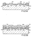
- the heavily doped n-type impurity regions 23a, 23b and 24 are formed in the silicon substrate 21, and the resultant structure of this stage is shown in Fig. 5A.
- Silicon oxide is, then, deposited on the entire surface of the structure by using a chemical vapor deposition technique, and the silicon oxide thus deposited provides the first inter-level insulating film 28.
- An appropriate photoresist mask is formed on the silicon oxide film, and the silicon oxide film is partially etched away so that the contact holes 29a and 29b are formed in the first inter-level insulating film 28 as shown in Fig. 5B.
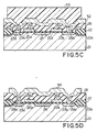
- a polysilicon film 52 is deposited on the entire surface of the structure by using a chemical vapor deposition technique, and a photoresist solution is, then, spun onto the polysilicon film 52.
- the photoresist film is baked and patterned so that a photoresist mask 53 is formed on the polysilicon film 52 as shown in Fig. 5C.
- the polysilicon film 52 is selectively removed so that a polysilicon strip 54 is left on the first inter-level insulating film 28 as shown in Fig. 5D.
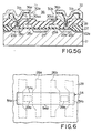
- the polysilicon strip 54 has a rectangular shape, and outer side edges 54a and 54b and longitudinal edges 54c and 54d defines the outer periphery of the polysilicon strip 54 as will be understood from Fig. 6. If the lower electrodes 30a and 30b is merged with each other, the resultant configuration is something like the polysilicon strip 54. This means that the side edges 30aa and 30bb do not take place in the polysilicon strip 54.
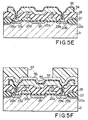
- the polysilicon strip 54 is covered with silicon oxide 55 as shown in Fig. 5E, and the silicon oxide film 55 may be produced through oxidation of the polysilicon strip 54.
- the dielectric film structure is constituted by a thin silicon nitride film sandwiched between thin silicon oxide films, chemical vapor deposition techniques may be used for formation of the dielectric film structure.
- a polysilicon film 56 is deposited on the entire surface of the structure, and a photoresist solution is spun onto the polysilicon film 56.
- a photoresist mask 57 is made from the photoresist film and defines the upper electrode 32. The resultant structure of this stage is shown in Fig. 5F.
- the photoresist mask 57 Using the photoresist mask 57, the polysilicon film 56, the silicon oxide film 55 and the polysilicon strip 54 are sequentially patterned by using anisotropical reactive ion etching technique, then the lower electrodes 30a and 30b, the dielectric film structures 31a and 31b and the upper electrode 32 are formed on the first inter-level insulating film 28. Since the photoresist mask 57 defines the upper electrode 32 as well as the lower electrodes 30a and 30b, the side edges 36a and 36b are substantially aligned with the side edges 30aa and 30bb as shown in Fig. 5G.
- a silicon oxide film is then deposited on the entire surface of the structure so that the second inter-level insulating film 33 covers the upper and lower electrodes 32, 30a and 30b.
- the contact hole 34 is formed in the second inter-level insulating film 33, and a refractory metal silicide, typically tungsten silicide, is deposited on the second inter-level insulating film 33.
- the refractory metal silicide film is patterned through a lithographic process, and the bit line 35 is formed on the second inter-level insulating film 33 as shown in Fig. 4.
- the photoresist mask 57 allows the side edges 30aa and 30bb of the lower electrodes 30a and 30b to be substantially aligned with the side edges 36a and 36b of the upper electrode 32.
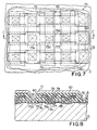
- FIGs. 7 and 8 of the drawings another random access memory device embodying the present invention is illustrated and fabricated on a lightly doped silicon substrate 71.
- the random access memory device shown in Figs. 7 and 8 is of the type disclosed in Japanese Patent Publication (Kokoku) No. 62-26116 and Digest of Technical Papers 1989, pages 238 and 239, and is featured by storage word lines. Namely, active regions (which are indicated by broken lines) are defined by a thick field oxide film 72, and heavily doped p-type channel stopper regions (not shown) are provided under the thick field oxide film 72.
- the heavily doped n-type impurity regions 73a and 73b are formed in one of the active regions, and are spaced from each other by a channel region which is covered with a thin gate oxide film 74.
- a word line 75 extends on the thin gate oxide film 74 and serves as a gate electrode of a switching transistor SW71.
- a first inter-level insulating film 76 covers the word line 75, and a contact hole 76a is formed in the first inter-level insulating film 76.
- a lower electrode 77 (which is indicated by dotted line) passes through the contact hole 76a and is brought into contact with the heavily doped n-type impurity region 73b.
- a dielectric film structure 78 covers the lower electrode 77, and a storage word line 79 is opposite to the lower electrode 77.
- the storage word line 79 is shared between the lower electrodes arranged in parallel to the word line 74 as an upper electrode.
- a second inter-level insulating film 80 covers the storage word line 79, and a contact hole 81 is formed in the first and second inter-level insulating films 76 and 80.
- a bit line 82 of tungsten silicide extends on the second inter-level insulating film 80 and is brought into contact with the heavily doped n-type impurity region 73a.
- a gate electrode 85 is provided over that area between adjacent storage capacitors, and the gate electrode 85 is maintained in a low voltage level so as to provide electrical isolation therebetween.
- the area between the adjacent storage capacitors may be doped with p-type impurity atoms for better isolation.
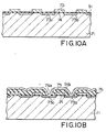
- N-type impurity atoms are ion-implanted into the silicon substrate 71 using the word line as a mask, and the heavily doped n-type impurity regions 73a and 73b are formed in the silicon substrate 71.
- the layout and the structure at this stage are shown in Figs. 9A and 10A, respectively.
- the first inter-level insulating film 76 is deposited on the entire surface of the structure, and the contact hole 76a is formed in the first inter-level insulating film 76.
- a polysilicon film is deposited on the entire surface of the structure and passes through the contact hole 76a to be brought into contact with the heavily doped n-type impurity region 73a.
- An appropriate photoresist mask is formed on the polysilicon film, and the polysilicon film is partially patterned with the photoresist mask. Namely, the photoresist mask on the polysilicon film only defines longitudinal ends, and the polysilicon film is shaped into a plurality of polysilicon strips 91a and 91b. The resultant structure at this stage is shown in Figs. 9B and 10B.
- the polysilicon strips 91a and 91b are covered with dielectric film structures 92a and 92b, and each of the dielectric film structures 92a and 92b is implemented by a thin silicon oxide film and a thin silicon nitride film.
- a polysilicon film 93 is deposited on the entire surface of the structure, and a photoresist solution is spun onto the polysilicon film 93.
- the photoresist film is patterned into a photomask 94 through a lithographic process, and the photoresist mask 94 defines the storage word lines 79.
- the resultant structure at this stage is shown in Figs. 9C and 10C.
- the polysilicon film 93, the dielectric film structures 92a and 92b and the polysilicon strips 91a and 91b are sequentially etched by using anisotropical reactive ion etching technique. Then, the storage word lines 79 and the lower electrodes 77 are formed in facing relationship to each other as described with reference to Figs. 7 and 8.
- a silicon oxide film is deposited on the entire surface of the structure as the second inter-level insulating film 80, and the contact hole 81 is formed in the first and second inter-level insulating films 76 and 80.
- a tungsten silicide film is deposited and patterned to form bit lines. As a result, the random access memory device shown in Figs. 7 and 8 is accomplished.
- the random access memory device thus fabricated has the storage capacitor with the lower electrode 77 substantially aligned with the storage word line 79, and, for this reason, the capacitance of the storage capacitor is increased without any occupation of additional real estate.
- FIG. 11 of the drawings still another random access memory device embodying the present invention is fabricated on a lightly doped p-type silicon substrate 101.
- the random access memory device shown in Fig. 11 is also of the type having storage word lines 102a, 102b and 102c faced to lower electrodes 103a, 103b and 103c through dielectric film structures 104a, 104b and 104c.
- the lower electrodes 103a to 103c are substantially aligned with the storage word lines 102a to 102c at the side edges thereof, and each storage capacitor occupies a relatively small amount of real estate.
- the lower electrodes 103b and 103c are held in contact with heavily doped n-type regions 105a and 105b, and a heavily doped p-type channel stopper region 106 and a thick field oxide film 107 are provided between the heavily doped n-type impurity regions 105a and 105b for electrical isolation.
Landscapes
- Engineering & Computer Science (AREA)
- Manufacturing & Machinery (AREA)
- Semiconductor Memories (AREA)
- Semiconductor Integrated Circuits (AREA)
Claims (3)
- Speichereinrichtung mit wahlfreiem Zugriff, die auf einem einzelnen Halbleitersubstrat (21) hergestellt ist und eine Vielzahl von Speicherzellen (M21, M22) aufweist, wobei jede Speicherzelle a) einen Schalttransistor (SW21/SW22) mit Störstellenbereichen (23a/23b, 24), die in dem Halbleitersubstrat mit Abständen ausgebildet sind, mit einer Gate-Isolierschicht (25a/26b), die in dem Bereich zwischen den Störstellenbereichen ausgebildet ist, und mit einer Gate-Elektrode (26a/26b), die auf dem Gate-Isolierfilm ausgebildet ist, und b) einen Speicherkondensator (STR21/STR22) mit einer unteren Elektrode (30a/30b), die über einem der Störstellenbereiche vorgesehen ist und in Kontakt mit einem der Störstellenbereiche gehalten ist, mit einer dielektrischen Schichtstruktur (31a/31b), die die untere Elektrode bedeckt, und mit einer oberen Elektrode (32), die in Berührung mit der dielektrischen Schichtstruktur gehalten wird, aufweist, dadurch gekennzeichnet, daß die obere Elektrode wenigstens mit einem Seitenrand (35a/35b) im wesentlichen mit einem Seitenrand (30aa/30bb) der unteren Elektrode ausgerichtet ist.
- Verfahren zum Herstellen einer Speichereinrichtung mit wahlfreiem Zugriff auf einem Halbleitersubstrat (21), das die Schritte aufweist:a) einen Gate-Isolierfilm (25a/25b) auf dem Halbleitersubstrat zu bilden;b) eine Gate-Elektrode (26a/26b) auf der Gate-Isolierschicht zu bilden;c) das Halbleitersubstrat mit Störstellenatomen zu dotieren, so daß Störstellenbereiche (23a/23b, 24) auf beiden Seiten der Gate-Elektrode in dem Halbleitersubstrat gebildet werden;d) eine in der Höhe dazwischen liegende Isolierschicht (28) zum Bedecken der Störstellenbereiche und der Gate-Elektrode zu bilden;e) ein Kontaktloch (29a/29b) in dem in der Höhe dazwischen liegenden Isolierfilm zu bilden, um einen Teil des einen der Störstellenbereiche (23a/23b) freizulegen; undf) einen Speicherkondensator (STR21/STR22) zu bilden, der in Kontakt mit einer der Störstellenbereiche gehalten wird;dadurch gekennzeichnet, daß Schritt f) beinhaltet, nacheinander eine erste leitende Schicht (54) auf der in der Höhe dazwischen liegenden Isolierschicht (28), eine dielektrische Schichtstruktur (55) auf der ersten leitenden Schicht (54) und eine zweite leitende Schicht (56) auf der dielektrischen Schichtstruktur (55) zu bilden, wobei wenigstens ein Seitenrand (36a/36b) der zweiten leitenden Schicht im wesentlichen mit einem Seitenrand (30aa/30bb) der ersten leitenden Schicht ausgerichtet ist.
- Verfahren nach Anspruch 2, bei dem wenigstens ein Seitenrand (36a/36b) der zweiten leitenden Schicht im wesentlichen mit dem einen Seitenrand (30aa/30bb) der ersten leitenden Schicht ausgerichtet wird, indem eine gemeinsame Maskenschicht (57), die auf der zweiten leitenden Schicht (56) ausgebildet wird, verwendet wird und nacheinander die zweite leitende Schicht (56), die dielektrische Schichtstruktur (55) und die erste leitende Schicht (54) strukturiert werden.
Applications Claiming Priority (2)
| Application Number | Priority Date | Filing Date | Title |
|---|---|---|---|
| JP25656/90 | 1990-02-05 | ||
| JP2025656A JPH03229459A (ja) | 1990-02-05 | 1990-02-05 | 半導体メモリおよびその製造方法 |
Publications (2)
| Publication Number | Publication Date |
|---|---|
| EP0443746A1 EP0443746A1 (de) | 1991-08-28 |
| EP0443746B1 true EP0443746B1 (de) | 1995-08-30 |
Family
ID=12171862
Family Applications (1)
| Application Number | Title | Priority Date | Filing Date |
|---|---|---|---|
| EP91300928A Expired - Lifetime EP0443746B1 (de) | 1990-02-05 | 1991-02-05 | Dynamische RAM-Einrichtung |
Country Status (5)
| Country | Link |
|---|---|
| US (1) | US5187549A (de) |
| EP (1) | EP0443746B1 (de) |
| JP (1) | JPH03229459A (de) |
| KR (1) | KR950003914B1 (de) |
| DE (1) | DE69112447T2 (de) |
Families Citing this family (5)
| Publication number | Priority date | Publication date | Assignee | Title |
|---|---|---|---|---|
| US20020023972A1 (en) * | 2000-06-13 | 2002-02-28 | Kah Carl L. C. | Closed case oscillating sprinkler |
| US5825609A (en) * | 1996-04-23 | 1998-10-20 | International Business Machines Corporation | Compound electrode stack capacitor |
| KR100230367B1 (ko) * | 1996-08-19 | 1999-11-15 | 윤종용 | 반도체 디바이스의 제조방법 |
| US5926718A (en) * | 1996-08-20 | 1999-07-20 | Micron Technology, Inc. | Method for forming a capacitor |
| KR19980064132A (ko) * | 1996-12-16 | 1998-10-07 | 윌리엄비.켐플러 | 동적 랜덤 액세스 메모리 어레이의 레이아웃 |
Family Cites Families (4)
| Publication number | Priority date | Publication date | Assignee | Title |
|---|---|---|---|---|
| JPS62202397A (ja) * | 1986-02-28 | 1987-09-07 | Fujitsu Ltd | 半導体記憶装置 |
| JPS63258060A (ja) * | 1987-04-15 | 1988-10-25 | Nec Corp | 半導体記憶装置 |
| JP2590171B2 (ja) * | 1988-01-08 | 1997-03-12 | 株式会社日立製作所 | 半導体記憶装置 |
| JP2723530B2 (ja) * | 1988-04-13 | 1998-03-09 | 日本電気株式会社 | ダイナミック型ランダムアクセスメモリ装置の製造方法 |
-
1990
- 1990-02-05 JP JP2025656A patent/JPH03229459A/ja active Pending
-
1991
- 1991-02-04 KR KR1019910001854A patent/KR950003914B1/ko not_active Expired - Fee Related
- 1991-02-05 US US07/651,065 patent/US5187549A/en not_active Expired - Fee Related
- 1991-02-05 EP EP91300928A patent/EP0443746B1/de not_active Expired - Lifetime
- 1991-02-05 DE DE69112447T patent/DE69112447T2/de not_active Expired - Fee Related
Also Published As
| Publication number | Publication date |
|---|---|
| US5187549A (en) | 1993-02-16 |
| DE69112447T2 (de) | 1996-02-29 |
| DE69112447D1 (de) | 1995-10-05 |
| JPH03229459A (ja) | 1991-10-11 |
| KR910016081A (ko) | 1991-09-30 |
| EP0443746A1 (de) | 1991-08-28 |
| KR950003914B1 (ko) | 1995-04-20 |
Similar Documents
| Publication | Publication Date | Title |
|---|---|---|
| KR900000207B1 (ko) | 반도체 기억장치와 그 제조방법 | |
| EP0444615B1 (de) | Dynamische Speicheranordnung mit wahlfreiem Zugriff mit Bitleitungen, die im Substrat vergraben sind | |
| KR910009788B1 (ko) | 다이나믹 랜덤 억세스 메모리 장치용 메모리셀의 층구조 및 그의 제조방법 | |
| US5321649A (en) | Stacked delta cell capacitor | |
| US4717942A (en) | Dynamic ram with capacitor groove surrounding switching transistor | |
| US5792683A (en) | Method for manufacturing of an SRAM device | |
| US4864464A (en) | Low-profile, folded-plate dram-cell capacitor fabricated with two mask steps | |
| JPH08250677A (ja) | 半導体記憶装置及びその製造方法 | |
| EP0488283B1 (de) | Verfahren zur Herstellung einer Speicherzelle für eine integrierte Halbleiterschaltung | |
| KR100289681B1 (ko) | 노드접촉으로부터오프셋된다중원통형축적전극을갖는비트라인상부에캐패시터셀을구비한반도체메모리장치및제조방법 | |
| US5156993A (en) | Fabricating a memory cell with an improved capacitor | |
| KR0151197B1 (ko) | 반도체 메모리장치 및 그 제조방법 | |
| KR950012034B1 (ko) | 반도체 기억장치의 제조방법 | |
| US5216267A (en) | Stacked capacitor dynamic random access memory with a sloped lower electrode | |
| US5459095A (en) | Method for making capacitor for use in DRAM cell using triple layers of photoresist | |
| EP0443746B1 (de) | Dynamische RAM-Einrichtung | |
| US5429976A (en) | Self-aligned method for forming polysilicon word lines on top of gate electrodes to increase capacitance of a stacked capacitor in a DRAM cell | |
| JP3108819B2 (ja) | 半導体記憶装置及びその製造方法 | |
| US5334547A (en) | Method of manufacturing a semiconductor memory having an increased cell capacitance in a restricted cell area | |
| KR960014970B1 (ko) | 반도체기억장치 및 그 제조방법 | |
| JPH0744274B2 (ja) | 半導体装置及びその製造方法 | |
| US6580175B1 (en) | Semiconductor layout structure for a conductive layer and contact hole | |
| JP3173046B2 (ja) | 半導体記憶装置の製造方法 | |
| JP2633577B2 (ja) | ダイナミックメモリセル及びその製造方法 | |
| JPH07193137A (ja) | 半導体記憶装置およびその製造方法 |
Legal Events
| Date | Code | Title | Description |
|---|---|---|---|
| PUAI | Public reference made under article 153(3) epc to a published international application that has entered the european phase |
Free format text: ORIGINAL CODE: 0009012 |
|
| 17P | Request for examination filed |
Effective date: 19910214 |
|
| AK | Designated contracting states |
Kind code of ref document: A1 Designated state(s): DE FR GB |
|
| 17Q | First examination report despatched |
Effective date: 19940919 |
|
| GRAA | (expected) grant |
Free format text: ORIGINAL CODE: 0009210 |
|
| AK | Designated contracting states |
Kind code of ref document: B1 Designated state(s): DE FR GB |
|
| REF | Corresponds to: |
Ref document number: 69112447 Country of ref document: DE Date of ref document: 19951005 |
|
| ET | Fr: translation filed | ||
| PLBE | No opposition filed within time limit |
Free format text: ORIGINAL CODE: 0009261 |
|
| STAA | Information on the status of an ep patent application or granted ep patent |
Free format text: STATUS: NO OPPOSITION FILED WITHIN TIME LIMIT |
|
| 26N | No opposition filed | ||
| PGFP | Annual fee paid to national office [announced via postgrant information from national office to epo] |
Ref country code: GB Payment date: 19990204 Year of fee payment: 9 |
|
| PGFP | Annual fee paid to national office [announced via postgrant information from national office to epo] |
Ref country code: FR Payment date: 19990209 Year of fee payment: 9 |
|
| PGFP | Annual fee paid to national office [announced via postgrant information from national office to epo] |
Ref country code: DE Payment date: 19990212 Year of fee payment: 9 |
|
| PG25 | Lapsed in a contracting state [announced via postgrant information from national office to epo] |
Ref country code: GB Free format text: LAPSE BECAUSE OF NON-PAYMENT OF DUE FEES Effective date: 20000205 |
|
| GBPC | Gb: european patent ceased through non-payment of renewal fee |
Effective date: 20000205 |
|
| PG25 | Lapsed in a contracting state [announced via postgrant information from national office to epo] |
Ref country code: FR Free format text: LAPSE BECAUSE OF NON-PAYMENT OF DUE FEES Effective date: 20001031 |
|
| PG25 | Lapsed in a contracting state [announced via postgrant information from national office to epo] |
Ref country code: DE Free format text: LAPSE BECAUSE OF NON-PAYMENT OF DUE FEES Effective date: 20001201 |
|
| REG | Reference to a national code |
Ref country code: FR Ref legal event code: ST |