EP0443746B1 - Dynamic random access memory device - Google Patents
Dynamic random access memory device Download PDFInfo
- Publication number
- EP0443746B1 EP0443746B1 EP91300928A EP91300928A EP0443746B1 EP 0443746 B1 EP0443746 B1 EP 0443746B1 EP 91300928 A EP91300928 A EP 91300928A EP 91300928 A EP91300928 A EP 91300928A EP 0443746 B1 EP0443746 B1 EP 0443746B1
- Authority
- EP
- European Patent Office
- Prior art keywords
- film
- random access
- impurity regions
- conductive film
- access memory
- Prior art date
- Legal status (The legal status is an assumption and is not a legal conclusion. Google has not performed a legal analysis and makes no representation as to the accuracy of the status listed.)
- Expired - Lifetime
Links
Images


Classifications
-
- H—ELECTRICITY
- H10—SEMICONDUCTOR DEVICES; ELECTRIC SOLID-STATE DEVICES NOT OTHERWISE PROVIDED FOR
- H10B—ELECTRONIC MEMORY DEVICES
- H10B12/00—Dynamic random access memory [DRAM] devices
-
- H—ELECTRICITY
- H10—SEMICONDUCTOR DEVICES; ELECTRIC SOLID-STATE DEVICES NOT OTHERWISE PROVIDED FOR
- H10B—ELECTRONIC MEMORY DEVICES
- H10B12/00—Dynamic random access memory [DRAM] devices
- H10B12/30—DRAM devices comprising one-transistor - one-capacitor [1T-1C] memory cells
- H10B12/31—DRAM devices comprising one-transistor - one-capacitor [1T-1C] memory cells having a storage electrode stacked over the transistor
Landscapes
- Semiconductor Memories (AREA)
- Semiconductor Integrated Circuits (AREA)
Description
- This invention relates to a dynamic random access memory device and, more particularly, to the structure of a stacked capacitor incorporated in each memory cell of the dynamic random access memory device.
- Various structures have been proposed for a dynamic random access memory cell of one-transistor one-capacitor type, and the transistor and the capacitor are called as "switching transistor" and "storage capacitor". The storage capacitor usually belongs to any one of three types, i.e. plane type, trench type and stacked type. The plane type capacitor has a MIS (Metal-Insulator-Semiconductor) structure fabricated partially in a semiconductor substrate and partially on the semiconductor substrate, and the trench type capacitor is formed in a narrow groove vertically extending from the major surface of a semiconductor substrate. The stacked type capacitor is fabricated over a semiconductor substrate and implemented by a lower electrode faced through a dielectric film to an upper electrode. The lower electrode is usually called as "memory electrode", and a data bit is stored therein in the form of electric charges. The upper electrode is usually shared with a plurality of dynamic random access memory cells and called as "opposite electrode".
- A typical example of the stacked type storage capacitor is disclosed in ISSCC 1987 Digest of Technical Papers pages 284 and 285. Figs. 1 and 2 show the structure of a known dynamic random access memory cell with a stacked type storage capacitor. The dynamic random access memory cell is fabricated on a p-type silicon substrate 1, and heavily doped
channel stoppers 2 are provided in the silicon substrate 1. A thickfield oxide film 3 partially covers the major surface of the silicon substrate 1 and defines an active area in the major surface. In the active area are formed a plurality of heavily doped n-type impurity regions common source region 5 and thedrain regions word lines 7a and 7b extend on the gate oxide films 6a and 6b as gate electrodes. Theword lines 7a and 7b or the gate electrodes are covered with a firstinter-level insulating layer 8, andcontact holes inter-level insulating layer 8. For better understanding, not only thecontact holes -
Memory electrodes 10a and 10b of polysilicon are formed on the firstinter-level insulating layer 8 and respectively project through thecontact holes drain regions memory electrodes 10a and 10b respectively, and anopposite electrode 12 of polysilicon is faced through the dielectric films 11a and 11b to thememory electrodes 10a and 10b and overlain by a secondinter-level insulating layer 13. A constant voltage level, typically, a power voltage level is supplied to theopposite electrode 12. - A
contact hole 14 is formed through the first and second inter-levelinsulating layers inter-level insulating layer 14. The bit line 15 passes through the contact hole 4 and is held in contact with thecommon source region 5. However, thebit line 5 is not shown in Fig. 1. The bit line 15 is formed of tungsten silicide and propagates a data bit fed thereto and therefrom. - The
drain region 4a, thecommon source region 5, the thin gate oxide film 6a and the gate electrode 7a form in combination a switching transistor SW1, and thememory electrode 10a, the dielectric film 11a and theopposite electrode 12 provide a stacked type storage capacitor STR1. The switching transistor SW1 and the storage capacitor STR1 as a whole constitute a random access memory cell M1. Similarly, thedrain region 4b, thecommon source region 5, the thin gate oxide film 6b and thegate electrode 7b form in combination a switching transistor SW2, and the memory electrode 10b, the dielectric film 11b and theopposite electrode 12 provide a stacked type storage capacitor STR2. The switching transistor SW2 and the storage capacitor STR2 as a whole constitute a random access memory cell M2. - In a prior art fabrication process, the
memory electrodes 10a and 10b are formed from a polysilicon film deposited on the firstinter-level insulating layer 8 with a mask layer. After formation of the dielectric films 11a and 11b, another polysilicon film is deposited over the entire surface of the structure, and the polysilicon film is patterned with another mask layer so as to form theopposite electrode 12. Thus, thememory electrodes 10a and 10b and theopposite electrode 12 are patterned by using different mask layers, and the mask layers are formed in a lithographic process with respective photo-masks. In general, the photo-masks are not perfectly aligned with each other in the lithographic process, a tolerance TL is usually provided to theopposite electrode 12, and, for this reason, the edge of theopposite electrode 12 inwardly projects from the edges of thememory electrodes 10a and 10b. The tolerance TL usually ranges from 0.3 micron to 0.4 micron. - A problem is encountered in the prior art random access memory device in that the tolerance TL consumes non-ignorable percentage of real estate assigned to each random access memory cell. Namely, the real estate assigned to each memory cell is of the order of 4 to 5 square-microns, and each
memory electrode 10a or 10b consumes an area of 1.0 micron by 1.5 micron. Since the length of 1.5 micron contains the tolerance TL, the tolerance TL wastes non-ignorable percentage of the area of 1.0 micron by 1.5 micron. In other words, the amount of electric charges accumulated in eachmemory electrode 10a or 10b or the capacitance of the storage capacitor STR1 or STR2 is relatively small for the real estate assigned to thememory electrode 10a or 10b, and, for this reason, a data bit memorized therein is not reliable. If the real estate assigned to each memory cell is further decreased for a larger integration density, the problem becomes more serious than now. - It is therefore an important object of the present invention to provide a random access memory device which has a stacked type storage capacitor formed without any tolerance.
- It is also an important object of the present invention to provide a process of fabricating a dynamic random access memory device through which lower and upper electrodes are aligned with each other without any tolerance.
- To accomplish these objects, the present invention proposes to provide an upper electrode aligned with a lower electrode. The upper electrode aligned with the lower electrode is formed through an etching stage for sequentially patterning the upper electrode, a dielectric film structure and a lower electrode using a single mask layer.
- In accordance with one aspect of the present invention, there is provided a random access memory device fabricated on a single semiconductor substrate and having a plurality of memory cells, each memory cell comprising a) a switching transistor having impurity regions formed in the semiconductor substrate at spacing, a gate insulating film formed on that area between the impurity regions, and a gate electrode formed on the gate insulating film, and b) a storage capacitor having a lower electrode provided over one of the impurity regions and held in contact with the aforesaid one of the impurity regions, a dielectric film structure covering the lower electrode, and an upper electrode held in contact with the dielectric film structure and having at least one side edge substantially aligned with one side edge of the lower electrode.
- In accordance with another aspect of the present invention, there is provided a process of fabricating a random access memory device on a semiconductor substrate, comprising the steps of:
- a) forming a gate insulating film on said semiconductor substrate;
- b) forming a gate electrode on said gate insulating film;
- c) doping said semiconductor substrate with impurity atoms so that impurity regions are formed on both sides of in said semiconductor substrate said gate electrode;
- d) forming an inter-level insulating film for covering said impurity regions and said gate electrode;
- e) forming a contact hole in said inter-level insulating film for exposing a part of said one of said impurity regions; and
- f) producing a storage capacitor held in contact with said one of said impurity regions,
- Preferably said at least one side edge of said second conductive film is substantially aligned with said one side edge of said first conductive film by using a common mask layer formed on said second conductive layer and sequentially patterning said second conductive film, said dielectric film structure and said first conductive film.
- The features and advantages of a dynamic random access memory device and a process of fabrication thereof according to the present invention will be more clearly understood from the following description taken in conjunction with the accompanying drawings in which:
- Fig. 1 is a plan view showing the layout of a prior art dynamic random access memory cell;
- Fig. 2 is a cross sectional view taken along line A-A of Fig. 1 and showing the structure of the prior art random access memory cell;
- Fig. 3 is a plan view showing the layout of a random access memory device according to the present invention;
- Fig. 4 is a cross sectional view taken along line B-B of Fig. 3 and showing the structure of the random access memory device;
- Figs. 5A to 5G are cross sectional views showing the sequence of a process for fabricating the random access memory device shown in Figs. 3 and 4;
- Fig. 6 is a plan view showing the layout of an intermediate structure shown in Fig. 5D;
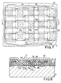
- Fig. 7 is a plan view showing the layout of another random access memory device according to the present invention;
- Fig. 8 is a cross sectional view taken along line C-C of Fig. 7 and showing the structure of the random access memory device;
- Fig. 9A to 9C are plan views showing the sequence of another process for fabricating the random access memory device shown in Figs. 7 and 8;
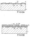
- Figs. 10A to 10C are cross sectional views taken along lines D-D to F-F and showing the intermediate structures of the random access memory device; and
- Fig. 11 is a cross sectional view showing the structure of still another random access memory device according to the present invention.
- Referring to Figs. 3 and 4 of the drawings, a random access memory device embodying the present invention is fabricated on a lightly doped p-
type silicon substrate 21, and a thickfield oxide film 22 is grown on the major surface of thesilicon substrate 21. Under the thickfield oxide film 22 is formed heavily doped p-typechannel stopper regions 22a which extend along the peripheries of the active areas, respectively. The thickfield oxide film 22 defines active areas in the major surface of thesilicon substrate 21, and two memory cells M21 and M22 are fabricated in one of the active areas. The memory cells M21 and M22 are of the one-transistor one-capacitor type, and, accordingly, each memory cell M21 or M22 is fabricated from a switching transistor SW21 or SW22 and a stacked type storage capacitor STR21 or STR22. - In the active area are formed heavily doped n-
type impurity regions gate oxide films gate electrodes gate oxide films gate oxide films word lines - A first inter-level insulating
film 28 covers theword lines contact holes film 28. The contact holes 29a and 29b reach the heavily doped n-type impurity regions film 28 are formedlower electrodes lower electrodes contact holes dielectric film structures lower electrodes upper electrode 32 is held in contact with thedielectric film structures lower electrodes upper electrode 32, or the opposite electrode, is shared between a plurality of memory cells including the memory cells M21 and M22. Theupper electrode 32 is covered with a second inter-level insulatingfilm 33, and anothercontact hole 34 is formed in the first and secondinter-level insulating films bit line 35 extends on the second inter-level insulatingfilm 33, and thebit line 35 passes through thecontact hole 34 so as to be brought into contact with the heavily doped n-type impurity region 24. Thebit line 35 is not shown in Fig. 3 so as to make the figure simple. - As will be better seen from Fig. 3, the
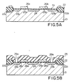
upper electrode 32 has arectangular aperture 36 partially defined by twoside edges lower electrodes upper electrode 32 with respect to thelower electrodes - Description is hereinbelow made on a process of fabricating the random access memory device shown in Figs. 3 and 4 with reference to Figs. 5A to 5G. The process sequence starts with the lightly doped p-
type silicon substrate 21, and p-type impurity atoms are selectively introduced into thesilicon substrate 21 through lithographic techniques. Thesilicon substrate 21 is thermally oxidized through a localized oxidation of silicon technique, and the heavily dopedchannel stopper regions 22a overlain by thefield oxide film 22 is formed in the major surface of thesilicon substrate 21. On a fresh surface of thesilicon substrate 21 is thermally grown a thin silicon oxide film which provides thegate oxide films gate electrodes gate oxide films silicon substrate 21 using thegate electrodes type impurity regions silicon substrate 21, and the resultant structure of this stage is shown in Fig. 5A. - Silicon oxide is, then, deposited on the entire surface of the structure by using a chemical vapor deposition technique, and the silicon oxide thus deposited provides the first inter-level insulating
film 28. An appropriate photoresist mask is formed on the silicon oxide film, and the silicon oxide film is partially etched away so that thecontact holes film 28 as shown in Fig. 5B. - Subsequently, a
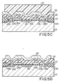
polysilicon film 52 is deposited on the entire surface of the structure by using a chemical vapor deposition technique, and a photoresist solution is, then, spun onto thepolysilicon film 52. The photoresist film is baked and patterned so that aphotoresist mask 53 is formed on thepolysilicon film 52 as shown in Fig. 5C. - Using the
photoresist mask 53, thepolysilicon film 52 is selectively removed so that apolysilicon strip 54 is left on the first inter-level insulatingfilm 28 as shown in Fig. 5D. Thepolysilicon strip 54 has a rectangular shape, andouter side edges longitudinal edges 54c and 54d defines the outer periphery of thepolysilicon strip 54 as will be understood from Fig. 6. If thelower electrodes polysilicon strip 54. This means that the side edges 30aa and 30bb do not take place in thepolysilicon strip 54. - The
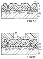
polysilicon strip 54 is covered withsilicon oxide 55 as shown in Fig. 5E, and thesilicon oxide film 55 may be produced through oxidation of thepolysilicon strip 54. However, if the dielectric film structure is constituted by a thin silicon nitride film sandwiched between thin silicon oxide films, chemical vapor deposition techniques may be used for formation of the dielectric film structure. - A
polysilicon film 56 is deposited on the entire surface of the structure, and a photoresist solution is spun onto thepolysilicon film 56. Aphotoresist mask 57 is made from the photoresist film and defines theupper electrode 32. The resultant structure of this stage is shown in Fig. 5F. - Using the
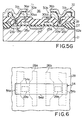
photoresist mask 57, thepolysilicon film 56, thesilicon oxide film 55 and thepolysilicon strip 54 are sequentially patterned by using anisotropical reactive ion etching technique, then thelower electrodes dielectric film structures upper electrode 32 are formed on the first inter-level insulatingfilm 28. Since thephotoresist mask 57 defines theupper electrode 32 as well as thelower electrodes - A silicon oxide film is then deposited on the entire surface of the structure so that the second inter-level insulating
film 33 covers the upper andlower electrodes contact hole 34 is formed in the second inter-level insulatingfilm 33, and a refractory metal silicide, typically tungsten silicide, is deposited on the second inter-level insulatingfilm 33. The refractory metal silicide film is patterned through a lithographic process, and thebit line 35 is formed on the second inter-level insulatingfilm 33 as shown in Fig. 4. - As will be understood from the foregoing description, the
photoresist mask 57 allows the side edges 30aa and 30bb of thelower electrodes upper electrode 32. - Turning to Figs. 7 and 8 of the drawings, another random access memory device embodying the present invention is illustrated and fabricated on a lightly doped
silicon substrate 71. The random access memory device shown in Figs. 7 and 8 is of the type disclosed in Japanese Patent Publication (Kokoku) No. 62-26116 and Digest of Technical Papers 1989, pages 238 and 239, and is featured by storage word lines. Namely, active regions (which are indicated by broken lines) are defined by a thickfield oxide film 72, and heavily doped p-type channel stopper regions (not shown) are provided under the thickfield oxide film 72. The heavily doped n-type impurity regions gate oxide film 74. Aword line 75 extends on the thingate oxide film 74 and serves as a gate electrode of a switching transistor SW71. A first inter-level insulatingfilm 76 covers theword line 75, and acontact hole 76a is formed in the first inter-level insulatingfilm 76. A lower electrode 77 (which is indicated by dotted line) passes through thecontact hole 76a and is brought into contact with the heavily doped n-type impurity region 73b. Adielectric film structure 78 covers thelower electrode 77, and astorage word line 79 is opposite to thelower electrode 77. Thestorage word line 79 is shared between the lower electrodes arranged in parallel to theword line 74 as an upper electrode. A second inter-level insulatingfilm 80 covers thestorage word line 79, and acontact hole 81 is formed in the first and secondinter-level insulating films bit line 82 of tungsten silicide extends on the second inter-level insulatingfilm 80 and is brought into contact with the heavily doped n-type impurity region 73a. Agate electrode 85 is provided over that area between adjacent storage capacitors, and thegate electrode 85 is maintained in a low voltage level so as to provide electrical isolation therebetween. The area between the adjacent storage capacitors may be doped with p-type impurity atoms for better isolation. - Description is made on a process of fabricating the random access memory device shown in Figs. 7 and 8 with reference to Figs. 9A to 9C and 10A to 10C. The process starts with the lightly doped p-
type silicon substrate 71, heavily doped p-type channel stopper regions and the thick filedoxide film 72 are, then, formed on the silicon substrate as similar to the first embodiment. A thinsilicon oxide film 91 is thermally grown on the active regions and partially provides thegate oxide film 74. A polysilicon film is deposited on the entire surface of the structure and is patterned through a lithographic process. Then, theword line 75, which partially provides the gate electrode, is formed on the field oxide film and the thinsilicon oxide film 91. N-type impurity atoms are ion-implanted into thesilicon substrate 71 using the word line as a mask, and the heavily doped n-type impurity regions silicon substrate 71. The layout and the structure at this stage are shown in Figs. 9A and 10A, respectively. - The first inter-level insulating
film 76 is deposited on the entire surface of the structure, and thecontact hole 76a is formed in the first inter-level insulatingfilm 76. A polysilicon film is deposited on the entire surface of the structure and passes through thecontact hole 76a to be brought into contact with the heavily doped n-type impurity region 73a. An appropriate photoresist mask is formed on the polysilicon film, and the polysilicon film is partially patterned with the photoresist mask. Namely, the photoresist mask on the polysilicon film only defines longitudinal ends, and the polysilicon film is shaped into a plurality of polysilicon strips 91a and 91b. The resultant structure at this stage is shown in Figs. 9B and 10B. The polysilicon strips 91a and 91b are covered withdielectric film structures dielectric film structures polysilicon film 93 is deposited on the entire surface of the structure, and a photoresist solution is spun onto thepolysilicon film 93. The photoresist film is patterned into aphotomask 94 through a lithographic process, and thephotoresist mask 94 defines the storage word lines 79. The resultant structure at this stage is shown in Figs. 9C and 10C. - The
polysilicon film 93, thedielectric film structures lower electrodes 77 are formed in facing relationship to each other as described with reference to Figs. 7 and 8. A silicon oxide film is deposited on the entire surface of the structure as the second inter-level insulatingfilm 80, and thecontact hole 81 is formed in the first and secondinter-level insulating films - The random access memory device thus fabricated has the storage capacitor with the
lower electrode 77 substantially aligned with thestorage word line 79, and, for this reason, the capacitance of the storage capacitor is increased without any occupation of additional real estate. - Turning to Fig. 11 of the drawings, still another random access memory device embodying the present invention is fabricated on a lightly doped p-type silicon substrate 101. The random access memory device shown in Fig. 11 is also of the type having
storage word lines electrodes dielectric film structures lower electrodes 103a to 103c are substantially aligned with thestorage word lines 102a to 102c at the side edges thereof, and each storage capacitor occupies a relatively small amount of real estate. - The
lower electrodes type regions 105a and 105b, and a heavily doped p-typechannel stopper region 106 and a thickfield oxide film 107 are provided between the heavily doped n-type impurity regions 105a and 105b for electrical isolation. - Although particular embodiments of the present invention have been shown and described, it will be obvious to those skilled in the art that various changes and modifications may be made without departing from the scope of the present invention.
characterised in that said step f) comprises sequentially forming a first conductive film on said inter-level insulating film, a dielectric film structure on said first conductive film, and a second conductive film on said dielectric film structure, at least one side edge of said second conductive film being substantially aligned with one side edge of said first conductive film.
Claims (3)
- A random access memory device fabricated on a single semiconductor substrate (21) and having a plurality of memory cells (M21, M22), each memory cell comprising a) a switching transistor (SW21/SW22) having impurity regions (23a/23b, 24) formed in said semiconductor substrate at spacing, a gate insulating film (25a/25b) formed on that area between said impurity regions, and a gate electrode (26a/26b) formed on said gate insulating film, and b) a storage capacitor (STR21/STR22) having a lower electrode (30a/30b) provided over one of said impurity regions and held in contact with said one of said impurity regions, a dielectric film structure (31a/ 31b) covering said lower electrode, and an upper electrode (32) held in contact with said dielectric film structure, characterized in that said upper electrode has at least one side edge (36a/ 36b) substantially aligned with one side edge (30aa /30bb) of said lower electrode.
- A process of fabricating a random access memory device on a semiconductor substrate (21), comprising the steps of:a) forming a gate insulating film (25a/25b) on said semiconductor substrate;b) forming a gate electrode (26a/26b) on said gate insulating film;c) doping said semiconductor substrate with impurity atoms so that impurity regions (23a/23b, 24) are formed on both sides of said gate electrode in said semiconductor substrate;d) forming an inter-level insulating film (28) for covering said impurity regions and said gate electrode;e) forming a contact hole (29a/29b) in said inter-level insulating film for exposing a part of said one of said impurity regions (23a/23b); andf) producing a storage capacitor (STR21/STR22) held in contact with said one of said impurity regions,characterised in that said step f) comprises sequentially forming a first conductive film (54) on said inter-level insulating film (28), a dielectric film structure (55) on said first conductive film (54), and a second conductive film (56) on said dielectric film structure (55), at least one side edge (36a/36b) of said second conductive film being substantially aligned with one side edge (30aa/30bb) of said first conductive film.
- The process of claim 2, in which said at least one side edge (36a/36b) of said second conductive film is substantially aligned with said one side edge (30aa/30bb) of said first conductive film by using a common mask layer (57) formed on said second conductive film (56) and sequentially patterning said second conductive film (56), said dielectric film structure (55) and said first conductive film (54).
Applications Claiming Priority (2)
| Application Number | Priority Date | Filing Date | Title |
|---|---|---|---|
| JP2025656A JPH03229459A (en) | 1990-02-05 | 1990-02-05 | Semiconductor memory and manufacture thereof |
| JP25656/90 | 1990-02-05 |
Publications (2)
| Publication Number | Publication Date |
|---|---|
| EP0443746A1 EP0443746A1 (en) | 1991-08-28 |
| EP0443746B1 true EP0443746B1 (en) | 1995-08-30 |
Family
ID=12171862
Family Applications (1)
| Application Number | Title | Priority Date | Filing Date |
|---|---|---|---|
| EP91300928A Expired - Lifetime EP0443746B1 (en) | 1990-02-05 | 1991-02-05 | Dynamic random access memory device |
Country Status (5)
| Country | Link |
|---|---|
| US (1) | US5187549A (en) |
| EP (1) | EP0443746B1 (en) |
| JP (1) | JPH03229459A (en) |
| KR (1) | KR950003914B1 (en) |
| DE (1) | DE69112447T2 (en) |
Families Citing this family (5)
| Publication number | Priority date | Publication date | Assignee | Title |
|---|---|---|---|---|
| US20020023972A1 (en) * | 2000-06-13 | 2002-02-28 | Kah Carl L. C. | Closed case oscillating sprinkler |
| US5825609A (en) * | 1996-04-23 | 1998-10-20 | International Business Machines Corporation | Compound electrode stack capacitor |
| KR100230367B1 (en) * | 1996-08-19 | 1999-11-15 | 윤종용 | Method for manufacturing semiconductor device |
| US5926718A (en) * | 1996-08-20 | 1999-07-20 | Micron Technology, Inc. | Method for forming a capacitor |
| KR19980064132A (en) * | 1996-12-16 | 1998-10-07 | 윌리엄비.켐플러 | Layout of a Dynamic Random Access Memory Array |
Family Cites Families (4)
| Publication number | Priority date | Publication date | Assignee | Title |
|---|---|---|---|---|
| JPS62202397A (en) * | 1986-02-28 | 1987-09-07 | Fujitsu Ltd | Semiconductor storage device |
| JPS63258060A (en) * | 1987-04-15 | 1988-10-25 | Nec Corp | Semiconductor memory divice |
| JP2590171B2 (en) * | 1988-01-08 | 1997-03-12 | 株式会社日立製作所 | Semiconductor storage device |
| JP2723530B2 (en) * | 1988-04-13 | 1998-03-09 | 日本電気株式会社 | Method for manufacturing dynamic random access memory device |
-
1990
- 1990-02-05 JP JP2025656A patent/JPH03229459A/en active Pending
-
1991
- 1991-02-04 KR KR1019910001854A patent/KR950003914B1/en not_active IP Right Cessation
- 1991-02-05 DE DE69112447T patent/DE69112447T2/en not_active Expired - Fee Related
- 1991-02-05 EP EP91300928A patent/EP0443746B1/en not_active Expired - Lifetime
- 1991-02-05 US US07/651,065 patent/US5187549A/en not_active Expired - Fee Related
Also Published As
| Publication number | Publication date |
|---|---|
| KR910016081A (en) | 1991-09-30 |
| DE69112447D1 (en) | 1995-10-05 |
| JPH03229459A (en) | 1991-10-11 |
| DE69112447T2 (en) | 1996-02-29 |
| US5187549A (en) | 1993-02-16 |
| KR950003914B1 (en) | 1995-04-20 |
| EP0443746A1 (en) | 1991-08-28 |
Similar Documents
| Publication | Publication Date | Title |
|---|---|---|
| EP0444615B1 (en) | Dynamic random access memory having bit lines buried in semiconductor substrate | |
| KR900000207B1 (en) | Semiconductor memory device with trench surrounding each memory cell | |
| KR910009788B1 (en) | Layer structure of memory cell for dynamic random access memory and method of fabrication thereof | |
| US5321649A (en) | Stacked delta cell capacitor | |
| US4717942A (en) | Dynamic ram with capacitor groove surrounding switching transistor | |
| US5792683A (en) | Method for manufacturing of an SRAM device | |
| US4864464A (en) | Low-profile, folded-plate dram-cell capacitor fabricated with two mask steps | |
| JPH08250677A (en) | Semiconductor memory device and its fabrication method | |
| EP0488283B1 (en) | Method of fabricating memory cell for semiconductor integrated circuit | |
| KR100289681B1 (en) | Semiconductor memory device having capacitor over bitline cell with multiple cylindrical storage electrode offset from node contact and process of fabrication thereof | |
| KR0151197B1 (en) | Semconductor device & its manufacturing method | |
| KR950012034B1 (en) | Method of manufacturing a semiconductor memory device | |
| US5459095A (en) | Method for making capacitor for use in DRAM cell using triple layers of photoresist | |
| EP0443746B1 (en) | Dynamic random access memory device | |
| US5216267A (en) | Stacked capacitor dynamic random access memory with a sloped lower electrode | |
| US5429976A (en) | Self-aligned method for forming polysilicon word lines on top of gate electrodes to increase capacitance of a stacked capacitor in a DRAM cell | |
| JP3108819B2 (en) | Semiconductor memory device and method of manufacturing the same | |
| US5334547A (en) | Method of manufacturing a semiconductor memory having an increased cell capacitance in a restricted cell area | |
| KR950000500B1 (en) | Manufacturing method and structure of dram cell capacitor | |
| KR960014970B1 (en) | Semiconductor memory device and manufacturing method thereof | |
| JPH0744274B2 (en) | Semiconductor device and manufacturing method thereof | |
| US6580175B1 (en) | Semiconductor layout structure for a conductive layer and contact hole | |
| JP3173046B2 (en) | Method for manufacturing semiconductor memory device | |
| JP2633577B2 (en) | Dynamic memory cell and method of manufacturing the same | |
| KR940009633B1 (en) | Manufacturing method of multi-layer capacitor of semiconductor memory device |
Legal Events
| Date | Code | Title | Description |
|---|---|---|---|
| PUAI | Public reference made under article 153(3) epc to a published international application that has entered the european phase |
Free format text: ORIGINAL CODE: 0009012 |
|
| 17P | Request for examination filed |
Effective date: 19910214 |
|
| AK | Designated contracting states |
Kind code of ref document: A1 Designated state(s): DE FR GB |
|
| 17Q | First examination report despatched |
Effective date: 19940919 |
|
| GRAA | (expected) grant |
Free format text: ORIGINAL CODE: 0009210 |
|
| AK | Designated contracting states |
Kind code of ref document: B1 Designated state(s): DE FR GB |
|
| REF | Corresponds to: |
Ref document number: 69112447 Country of ref document: DE Date of ref document: 19951005 |
|
| ET | Fr: translation filed | ||
| PLBE | No opposition filed within time limit |
Free format text: ORIGINAL CODE: 0009261 |
|
| STAA | Information on the status of an ep patent application or granted ep patent |
Free format text: STATUS: NO OPPOSITION FILED WITHIN TIME LIMIT |
|
| 26N | No opposition filed | ||
| PGFP | Annual fee paid to national office [announced via postgrant information from national office to epo] |
Ref country code: GB Payment date: 19990204 Year of fee payment: 9 |
|
| PGFP | Annual fee paid to national office [announced via postgrant information from national office to epo] |
Ref country code: FR Payment date: 19990209 Year of fee payment: 9 |
|
| PGFP | Annual fee paid to national office [announced via postgrant information from national office to epo] |
Ref country code: DE Payment date: 19990212 Year of fee payment: 9 |
|
| PG25 | Lapsed in a contracting state [announced via postgrant information from national office to epo] |
Ref country code: GB Free format text: LAPSE BECAUSE OF NON-PAYMENT OF DUE FEES Effective date: 20000205 |
|
| GBPC | Gb: european patent ceased through non-payment of renewal fee |
Effective date: 20000205 |
|
| PG25 | Lapsed in a contracting state [announced via postgrant information from national office to epo] |
Ref country code: FR Free format text: LAPSE BECAUSE OF NON-PAYMENT OF DUE FEES Effective date: 20001031 |
|
| PG25 | Lapsed in a contracting state [announced via postgrant information from national office to epo] |
Ref country code: DE Free format text: LAPSE BECAUSE OF NON-PAYMENT OF DUE FEES Effective date: 20001201 |
|
| REG | Reference to a national code |
Ref country code: FR Ref legal event code: ST |