EP0442212B1 - Verfahren zur Erzeugung eines Magnetwandlers in Dünnfilmtechnik - Google Patents
Verfahren zur Erzeugung eines Magnetwandlers in Dünnfilmtechnik Download PDFInfo
- Publication number
- EP0442212B1 EP0442212B1 EP90313689A EP90313689A EP0442212B1 EP 0442212 B1 EP0442212 B1 EP 0442212B1 EP 90313689 A EP90313689 A EP 90313689A EP 90313689 A EP90313689 A EP 90313689A EP 0442212 B1 EP0442212 B1 EP 0442212B1
- Authority
- EP
- European Patent Office
- Prior art keywords
- layer
- magnetic
- thin film
- gap material
- pole tip
- Prior art date
- Legal status (The legal status is an assumption and is not a legal conclusion. Google has not performed a legal analysis and makes no representation as to the accuracy of the status listed.)
- Expired - Lifetime
Links
Images


Classifications
-
- G—PHYSICS
- G11—INFORMATION STORAGE
- G11B—INFORMATION STORAGE BASED ON RELATIVE MOVEMENT BETWEEN RECORD CARRIER AND TRANSDUCER
- G11B5/00—Recording by magnetisation or demagnetisation of a record carrier; Reproducing by magnetic means; Record carriers therefor
- G11B5/127—Structure or manufacture of heads, e.g. inductive
- G11B5/31—Structure or manufacture of heads, e.g. inductive using thin films
- G11B5/3163—Fabrication methods or processes specially adapted for a particular head structure, e.g. using base layers for electroplating, using functional layers for masking, using energy or particle beams for shaping the structure or modifying the properties of the basic layers
-
- Y—GENERAL TAGGING OF NEW TECHNOLOGICAL DEVELOPMENTS; GENERAL TAGGING OF CROSS-SECTIONAL TECHNOLOGIES SPANNING OVER SEVERAL SECTIONS OF THE IPC; TECHNICAL SUBJECTS COVERED BY FORMER USPC CROSS-REFERENCE ART COLLECTIONS [XRACs] AND DIGESTS
- Y10—TECHNICAL SUBJECTS COVERED BY FORMER USPC
- Y10T—TECHNICAL SUBJECTS COVERED BY FORMER US CLASSIFICATION
- Y10T29/00—Metal working
- Y10T29/49—Method of mechanical manufacture
- Y10T29/49002—Electrical device making
- Y10T29/4902—Electromagnet, transformer or inductor
- Y10T29/49021—Magnetic recording reproducing transducer [e.g., tape head, core, etc.]
- Y10T29/49032—Fabricating head structure or component thereof
- Y10T29/49036—Fabricating head structure or component thereof including measuring or testing
- Y10T29/49043—Depositing magnetic layer or coating
- Y10T29/49044—Plural magnetic deposition layers
-
- Y—GENERAL TAGGING OF NEW TECHNOLOGICAL DEVELOPMENTS; GENERAL TAGGING OF CROSS-SECTIONAL TECHNOLOGIES SPANNING OVER SEVERAL SECTIONS OF THE IPC; TECHNICAL SUBJECTS COVERED BY FORMER USPC CROSS-REFERENCE ART COLLECTIONS [XRACs] AND DIGESTS
- Y10—TECHNICAL SUBJECTS COVERED BY FORMER USPC
- Y10T—TECHNICAL SUBJECTS COVERED BY FORMER US CLASSIFICATION
- Y10T29/00—Metal working
- Y10T29/49—Method of mechanical manufacture
- Y10T29/49002—Electrical device making
- Y10T29/4902—Electromagnet, transformer or inductor
- Y10T29/49021—Magnetic recording reproducing transducer [e.g., tape head, core, etc.]
- Y10T29/49032—Fabricating head structure or component thereof
- Y10T29/49036—Fabricating head structure or component thereof including measuring or testing
- Y10T29/49043—Depositing magnetic layer or coating
- Y10T29/49046—Depositing magnetic layer or coating with etching or machining of magnetic material
-
- Y—GENERAL TAGGING OF NEW TECHNOLOGICAL DEVELOPMENTS; GENERAL TAGGING OF CROSS-SECTIONAL TECHNOLOGIES SPANNING OVER SEVERAL SECTIONS OF THE IPC; TECHNICAL SUBJECTS COVERED BY FORMER USPC CROSS-REFERENCE ART COLLECTIONS [XRACs] AND DIGESTS
- Y10—TECHNICAL SUBJECTS COVERED BY FORMER USPC
- Y10T—TECHNICAL SUBJECTS COVERED BY FORMER US CLASSIFICATION
- Y10T29/00—Metal working
- Y10T29/49—Method of mechanical manufacture
- Y10T29/49002—Electrical device making
- Y10T29/4902—Electromagnet, transformer or inductor
- Y10T29/49021—Magnetic recording reproducing transducer [e.g., tape head, core, etc.]
- Y10T29/49032—Fabricating head structure or component thereof
- Y10T29/4906—Providing winding
- Y10T29/49064—Providing winding by coating
Definitions
- This invention relates to a method of manufacturing thin film magnetic transducers.
- Thin film magnetic read/write heads are used for magnetically reading and writing information upon a magnetic storage medium such as a magnetic disk or magnetic tape. It is highly desirable to provide a high density of information storage on the magnetic storage medium.
- Increased storage density in a recording system may be achieved by providing an areal density as high as possible for a given recording surface.
- the areal density is found by multiplying the number of flux reversals per unit length along the track (linear density in units of flux reversals per unit length e.g. inch) by the number of tracks available per unit length in the radial direction (track density in units of tracks per unit length e.g. inch).
- a technique which provides better pole alignment begins with a top pole, bottom pole and a gap area separating the top and bottom poles, all fabricated substantially wider than desired.
- a narrower mask layer is then deposited upon the upper pole.
- the structure is then aligned using a material removal process ("milling") such as ion milling or reactive ion milling in which high energy ions bombard the pole tip region to remove the excess material (top pole, bottom pole and gap material) that extends beyond the edges of the masking layer.
- the masking layer protects only a portion of the top pole, bottom pole and gap so that the width of the completed pole tips is approximately the same as the width of the masking layer.
- the present invention seeks to provide closely aligned pole tips in a thin film magnetic transducer allowing increased data storage densities.
- a method of manufacturing a thin film magnetic transducer characterised by comprising: forming a first magnetic layer on a non-magnetic substrate; forming a gap material layer on the first magnetic layer; depositing a layer having an aperture of a defined structure upon the gap material layer; forming a second magnetic layer over the gap material layer and in the aperture; depositing a sacrificial mask layer on the second magnetic layer and in the aperture; removing the layer having an aperture, exposing a portion of the gap material layer and a portion of the first magnetic layer; and exposing the thin film magnetic transducer to a material removal process.
- the step of depositing the sacrificial mask layer comprises depositing first and second sacrificial mask layers, the first sacrificial mask layer being sandwiched between the second sacrificial mask layer and the second magnetic layer.
- the step of exposing the thin film magnetic transducer to a material removal process may comprise ion milling, preferably reactive ion milling or sputter etching.
- the first and/or second magnetic layer may have a thickness in the range of from about 1 micron to about 5 microns.
- the gap material layer may have a thickness in the range from about 0.1 microns to about 1 micron.
- the sacrificial mask layer may have a thickness in the range from about 1 micron to about 7 microns.
- Magnetic heads are now fabricated in a manner similar to that used for semi-conductor integrated circuits in the electronics industry. Many thin film heads are deposited across a wafer or substrate using etching and photo-lithographic techniques. The wafer may then be sliced into many microscopic individual magnetic heads for use with magnetic storage devices such magnetic disks.
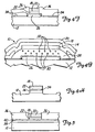
- Figure 1 shows a top view of a thin film magnetic transducer or head 10 according to the present invention prior to removal of a sacrificial mask layer.
- Figure 1 includes a substrate 12, an upper pole piece 14 having a paddle shape and lower layers indicated collectively at 16.
- the substrate 12 typically comprises a ceramic compound such as Al 2 O 3 -TiC.
- the thin film magnetic head of Figure 1 is shown in cross section in Figure 2.
- the upper pole piece 14 is shown covered with two sacrificial mask layers 18, 20 in Figure 2.
- the upper pole piece 14 includes an upper pole tip 22.
- the thin film magnetic head 10 also includes a lower pole piece 24 having a lower pole tip 26.
- the upper and lower pole pieces 14, 24 are formed of magnetic thin films such as, for example, NiFe.
- the area between the upper pole piece 14 and the lower pole piece 24 is filled with an insulator 28. Embedded within the insulator 28 are conductors 30, 32. The area between the upper pole tip 22 and the lower pole tip 26 is filled with gap material 34, typically comprising Al 2 O 3 .
- the upper pole piece 14 and the lower pole piece 24 contact each other at a back gap "via" (not shown) and form the two poles of a thin film magnetic transducer or head.
- the conductors 30, 32 are formed in a coil through the region between the upper pole piece 14 and the lower pole piece 24 and extend around the back gap via.
- a magnetic field is induced in the upper and lower pole pieces 14, 24. This magnetic field extends between the upper and lower pole tips 22, 26 and through the gap material 34.
- a magnetic fringe field is formed extending beyond the boundaries of the upper and lower pole tips 22, 26.
- a magnetic storage medium If a magnetic storage medium is passed through this fringe field, the magnetic flux emanating from the upper and lower pole tips 22, 26 will impress a magnetic field upon the surface of the magnetic storage medium. Conversely, if a magnetic field, such as that produced by a magnetic storage medium, is passed through the fringe field region of the thin film magnetic head 10, a magnetic field will be induced in the upper and lower pole pieces 14, 24 and through the back gap via. This changing magnetic field will induce an electric current to flow through the conductors 30, 32. The electric current is then sensed using electrical equipment and converted into an information signal to recover information stored upon the magnetic storage medium.
- Figure 3 is a cross sectional view of a thin film magnetic head 10 showing the pole tip region of Figure 2.
- Sacrificial mask layers 18, 20 cover the upper pole tip 22 while leaving a portion of the gap material 34 and the lower pole tip 26 uncovered or exposed.
- the sacrificial mask layers 18, 20 may comprise nickel/iron (NiFe), copper or nickel/phosphorous (Nip).
- NiFe nickel/iron
- Nip nickel/phosphorous
- a milling process removes the exposed gap material 34 and the lower pole tip 26 along with the sacrificial mask layers 18, 20 to leave the upper pole tip 22 intact along with the protected portion of the gap material 34 and the lower pole tip 26.
- the gap material 34 may range in thickness between about 0.1 microns and about 1 micron, the pole tips 22, 26 between about 1 micron and about 5 microns, and the total sacrificial mask thickness from about 1 micron to about 7 microns.
- Figures 4A to 4H detail the steps of a method according to the present invention used to form the structure of Figure 3 having the sacrificial mask layers 18, 20 aligned with the upper pole tip 22.
- Figure 4A is a cross sectional view of the substrate 12 upon which a deposition process takes place.
- the substrate 12 is generally very large relative to the thin film magnetic head 10 so that many replicas of the thin film magnetic head may be deposited across the entire surface of the substrate 12.
- Figure 4B shows the substrate 12 of Figure 4A including the lower pole tip 26 deposited upon the substrate 12 using photo-lithographic techniques.
- the view of Figure 4B shows the width of the lower pole tip 26.
- Figure 4C depicts the lower pole tip 26 including a layer of gap material 34 which also covers a portion of the substrate 12.
- the gap material 34 typically comprises Al 2 O 3 .
- FIG 4D two photo-resist dams 36 have been deposited upon the gap material 34 while leaving uncovered the area where the upper pole tip 22 will be deposited. Not shown in Figure 4D is that the photo-resist dams 36 do not cover the entire surface shown in Figures 1 and 2 and leave exposed the portion of the thin film magnetic head 10 where the upper pole piece 14 is to be desposited.
- the photo-resist dams 36 may be deposited using standard photo-lithographic and masking techniques.
- the upper pole piece 14 and the upper pole tip 22 are then deposited in the area between the photo-resist dams 36 upon the exposed portion of the gap material 34 as shown in Figure 4E.
- Figure 4F shows the pole tip region following deposition of the sacrificial mask layers 18, 20.
- Figure 4G depicts a cross section of Figure 1 taken in the middle portion of the thin film magnetic head 10 along the line 4G - 4G following the deposition of the sacrificial mask layers 18, 20.
- the sacrificial mask layer 20 may comprise any platable non-magnetic metal.
- the sacrificial mask layers may be chosen, for example, to the milling corresponding to the milling rates lower pole 26 and gap material 34, although other materials may be employed.
- Figure 4G shows that the thin film magnetic head 10 is completely covered and protected by the sacrificial mask layers 18, 20 everywhere except the area near the pole tip region where the exposed portion of the gap material 34 and the exposed portion of the lower pole tip 26 are to be removed, as shown in Figure 3.
- the photo-resist dams 36 shown in Figure 4F are removed using a chemical etching process, which leaves the structure surrounding the pole tip area as shown in Figure 3.
- the second sacrificial mask layer may also be used to protect the conductors during the milling process.
- the photo-resist dams 36 shown in Figure 4D to 4F actually extend around the entire paddle shape of the thin film magnetic head. Before the first sacrificial layer is deposited upon the upper pole tip, the portion of the photo-resist dams that is not near the pole tips is removed by exposure to radiation followed by chemical development. The relief area left by this photo-resist may then be covered over with the second sacrificial layer, to protect the conductors as shown in Figure 4G. Following milling, the second sacrificial layer may then be removed.
- the pole tip region shown in Figure 3 (and consequently the thin film magnetic head 10) is then exposed to a material removal ("milling") process in which the unprotected areas of the thin film magnetic head 10 are milled away along with the sacrificial layers 18, 20.
- the milling process preferably comprising ion milling, in which argon or xenon ions are produced by an ion source and accelerated by an electric field through an electrified grid.
- Other ion sources may be used, as well as reactive ion milling in which the milling ions react with the milled material.
- Chemical etching or sputter etching may also be used for material removal.
- the energetic ions produced by the ion milling device bombard the surface of the thin film magnetic head 10 to remove a portion of the material they impact. This milling process removes the exposed areas of the gap material 34 and the lower pole tip 26 as well as the sacrificial layers 18, 20.
- the sacrificial layers 18, 20 must have a thickness and a milling rate so that the thin film magnetic head 10 and the upper pole tip 22 are protected during the milling process.
- the materials comprising the sacrificial masks 18, 20 are chosen to correspond to the lower pole tip 26 and the gap material 34.
- the resultant pole tip structure is shown in Figure 4H.
- the non-aligned portions of the gap material 34 and the lower pole tip 26 have been removed by the milling process.
- the milling process also removes all of the sacrificial layer 20 along with the majority of the sacrificial layer 18 when the thickness and milling rate of the sacrificial layers 18, 20 is optimised. If desired, the remaining portion of the sacrificial layer 18 may be removed through a process such as chemical etching.
- the present invention may also be used when the lower pole tip and the gap material have "infinite width".
- Figure 5 a cross section of a pole tip region having an infinite width, the lower pole tip 38 and the gap material 40 is shown.
- the upper pole tip 22, the sacrificial mask layers 18, 20 and the photo-resist dams 36 are deposited as described above.
- the photo-resist dams 36 are then chemically etched to leave the non-aligned portion of the lower pole tip 38 and the gap material 40 exposed and the aligned portion of the lower pole tip 38 and the gap material 40 covered by the upper pole tip 22 and the sacrificial layers 18, 20.
- a milling process is then applied as described above, and the non-aligned, exposed portions of the gap material 40 and the lower pole tip 38 are milled away while the upper pole tip 22, the aligned portions of the gap material 40 and the lower pole tip 38 are protected by the sacrificial layers 18, 20.
- the pole tip structure resulting from the milling process is similar to that shown in Figure 4H.
- Figure 6 shows a pole tip structure comprising a lower pole tip 42 formed in a substrate 44 using a method according to the present invention.
- the substrate 44 comprises magnetic ferrite.
- the lower pole tip 42 is formed in the substrate 44 because a sacrificial mask layer 46 protects an upper pole tip 48, a gap material layer 50 and a lower pole tip 42.
- the sacrificial mask layer 46 is formed using the self alignment techniques of a method according to the present invention.
- the present invention produces thin film pole tips in vertical alignment which have similar widths. Even if the accuracy of the alignment between the upper and lower pole tips is poor due to the accuracy and definition of the deposition technique, the present invention provides a method to shape the pole tips and gap material so that these deficiencies are overcome. The present invention reduces time and provides cost savings in this shaping process. Because only two layers (the layer of the gap material and the layer of the pole tip) are milled, milling times are reduced along with mask thickness. Manufacturing time and cost are also reduced because only a single pair of photo-resist dams are used to form both the upper pole tip and the sacrificial mask.
Landscapes
- Engineering & Computer Science (AREA)
- Manufacturing & Machinery (AREA)
- Magnetic Heads (AREA)
Claims (7)
- Verfahren zur Herstellung eines Dünnfilm-Magnetwandlers (10),
gekennzeichnet durch die folgenden Schritte: Ausbilden einer ersten magnetischen Schicht (26;42) auf einem nichtmagnetischen Substrat (12;44) ; Ausbildung einer Spaltmaterialschicht (34;50) auf der ersten magnetischen Schicht (26;42); Abscheiden einer Schicht (36) mit einer Öffnung mit einer definierten Struktur auf der Spaltmaterialschicht (34;50); Ausbildung einer zweiten magnetischen Schicht (22;48) über der Spaltmaterialschicht und in der Öffnung; Abscheiden einer Opfermaskenschicht (18,20;46) auf der zweiten magnetischen Schicht (22;48) und in der Öffnung; Entfernen der eine Öffnung aufweisenden Schicht (36), Freilegen eines Teils der Spaltmaterialschicht (34;50) und eines Teils der ersten magnetischen Schicht (26;42) ; und Beaufschlagen des Dünnfilm-Magnetwandlers (10) mit einem Materialentfernungsprozess. - Verfahren zur Herstellung eines Dünnfilm-Magnetwandlers (10) nach Anspruch 1, gekennzeichnet durch:
die Ausbildung der ersten magnetischen Schicht (26;42) als Teil eines Hauptkörperbereiches und eines Teils eines Polspitzenbereichs auf dem Substrat (12,44); die Abscheidung der Spaltmaterialschicht (34;50) auf der ersten magnetischen Schicht in dem Polspitzenbereich; und die Abscheidung einer nichtmagnetischen Isolierschicht (28) auf der ersten magnetischen Schicht (26;42) in dem Hauptkörperbereich vor dem Abscheiden der Schicht (36), wobei die nichtmagnetische Isolierschicht eine Vielzahl von elektrischen Leitern (30,32) trägt, die sich durch diese erstrecken. - Verfahren nach einem der vorhergehenden Ansprüche,
dadurch gekennzeichnet, daß der Schritt der Abscheidung der Opfermaskenschicht die Abscheidung erster und zweiter Opfermaskenschichten (18,20) umfaßt, wobei die erste Opfermaskenschicht (18) zwischen der zweiten Opfermaskenschicht (20) und der zweiten Magnetschicht (22) eingeschichtet ist. - Verfahren nach einem der vorhergehenden Ansprüche,
dadurch gekennzeichnet, daß der Schritt der Beaufschlagung des Dünnfilm-Magnetwandlers (10) mit einem Materialentfernungsprozess das Ionenfräsen, vorzugsweise das reaktive Ionenfräsen, oder eine Zerstäubungsätzung umfaßt. - Verfahren nach einem der Ansprüche 2-4,
dadurch gekennzeichnet, daß die erste und/oder zweite magnetische Schicht (26;22;42;48) eine Dicke im Bereich von ungefähr 1 Mikrometer bis ungefähr 5 Mikrometer aufweist. - Verfahren nach einem der vorhergehenden Ansprüche,
dadurch gekennzeichnet, daß die Spaltmaterialschicht (34;50) eine Dicke im Bereich von ungefähr 0,1 Mikrometer bis ungefähr 1 Mikrometer hat. - Verfahren nach einem der vorhergehenden Ansprüche,
dadurch gekennzeichnet, daß die Opfermaskenschicht (18,20;46) eine Dicke im Bereich von ungefähr 1 Mikrometer bis ungefähr 7 Mikrometer hat.
Applications Claiming Priority (2)
| Application Number | Priority Date | Filing Date | Title |
|---|---|---|---|
| US480278 | 1990-02-15 | ||
| US07/480,278 US4992901A (en) | 1990-02-15 | 1990-02-15 | Self aligned magnetic poles using sacrificial mask |
Publications (3)
| Publication Number | Publication Date |
|---|---|
| EP0442212A2 EP0442212A2 (de) | 1991-08-21 |
| EP0442212A3 EP0442212A3 (en) | 1993-01-20 |
| EP0442212B1 true EP0442212B1 (de) | 1999-02-03 |
Family
ID=23907350
Family Applications (1)
| Application Number | Title | Priority Date | Filing Date |
|---|---|---|---|
| EP90313689A Expired - Lifetime EP0442212B1 (de) | 1990-02-15 | 1990-12-14 | Verfahren zur Erzeugung eines Magnetwandlers in Dünnfilmtechnik |
Country Status (6)
| Country | Link |
|---|---|
| US (1) | US4992901A (de) |
| EP (1) | EP0442212B1 (de) |
| JP (1) | JPH0778859B2 (de) |
| KR (1) | KR100264700B1 (de) |
| DE (1) | DE69032935T2 (de) |
| SG (1) | SG44623A1 (de) |
Families Citing this family (33)
| Publication number | Priority date | Publication date | Assignee | Title |
|---|---|---|---|---|
| US5079035A (en) * | 1989-10-10 | 1992-01-07 | International Business Machines Corporation | Method of making a magnetoresistive read transducer having hard magnetic bias |
| US5141623A (en) * | 1990-02-15 | 1992-08-25 | Seagate Technology, Inc. | Method for aligning pole tips in a thin film head |
| JPH0410208A (ja) * | 1990-04-27 | 1992-01-14 | Hitachi Ltd | 薄膜磁気ヘッド及びその製造方法 |
| US5084957A (en) * | 1990-11-06 | 1992-02-04 | Seagate Technology, Inc. | Method for aligning thin film head pole tips |
| US5137750A (en) * | 1990-11-06 | 1992-08-11 | Seagate Technology, Inc. | Method of making a thin film head with contoured pole face edges for undershoot reduction |
| US5256249A (en) * | 1991-09-17 | 1993-10-26 | Seagate Technology, Inc. | Method of manufacturing a planarized magnetoresistive sensor |
| US5283942A (en) * | 1992-12-29 | 1994-02-08 | International Business Machines Corporation | Sacrificial layer planarization process for fabricating a narrow thin film inductive head |
| US5452166A (en) * | 1993-10-01 | 1995-09-19 | Applied Magnetics Corporation | Thin film magnetic recording head for minimizing undershoots and a method for manufacturing the same |
| US5699605A (en) * | 1994-05-23 | 1997-12-23 | Seagate Technology, Inc. | Method for forming a magnetic thin film head with recessed basecoat |
| US5572392A (en) * | 1994-11-17 | 1996-11-05 | International Business Machines Corporation | Arbitrary pattern write head assembly for writing timing-based servo patterns on magnetic storage media |
| US5901431A (en) * | 1995-06-07 | 1999-05-11 | International Business Machines Corporation | Method of fabricating a thin film inductive head having a second pole piece having a mushroom yoke portion |
| US5578342A (en) * | 1995-07-05 | 1996-11-26 | Read-Rite Corporation | Alignment of magnetic poles of thin film transducer |
| JP3349925B2 (ja) * | 1996-09-10 | 2002-11-25 | アルプス電気株式会社 | 薄膜磁気ヘッドの製造方法 |
| JP2953401B2 (ja) * | 1996-10-04 | 1999-09-27 | 日本電気株式会社 | 磁気抵抗効果型複合ヘッドの製造方法 |
| US5804085A (en) * | 1997-01-30 | 1998-09-08 | Quantum Corporation | Process for producing a pole-trimmed writer in a magnetoresistive read/write head and a data transducer made thereby |
| JP3466041B2 (ja) * | 1997-03-03 | 2003-11-10 | アルプス電気株式会社 | 磁気ヘッドおよびその製造方法 |
| JPH10247305A (ja) * | 1997-03-03 | 1998-09-14 | Sanyo Electric Co Ltd | 複合型薄膜磁気ヘッドの製造方法 |
| JPH117608A (ja) * | 1997-04-25 | 1999-01-12 | Fujitsu Ltd | 磁気ヘッド及びその製造方法 |
| US5916423A (en) * | 1997-05-06 | 1999-06-29 | International Business Machines Corporation | P1 notched write head with minimum overmilled p1 and p2 |
| US6586049B2 (en) * | 1997-08-28 | 2003-07-01 | Tdk Corporation | Patterning method using mask and manufacturing method for composite type thin film magnetic head using the patterning method |
| US6031695A (en) * | 1997-09-05 | 2000-02-29 | International Business Machines Corporation | Combined read head and write head with non-magnetic electrically conductive layer on upper pole tip thereof |
| US5940250A (en) * | 1997-10-21 | 1999-08-17 | Maxtor Corporation | Disk drive head having a read wide/write narrow architecture |
| US6158107A (en) * | 1998-04-02 | 2000-12-12 | International Business Machines Corporation | Inverted merged MR head with plated notched first pole tip and self-aligned second pole tip |
| US6055138A (en) * | 1998-05-06 | 2000-04-25 | Read-Rite Corporation | Thin film pedestal pole tips write head having narrower lower pedestal pole tip |
| US6490125B1 (en) | 1999-04-09 | 2002-12-03 | Read-Rite Corporation | Thin film write head with improved yoke to pole stitch |
| AU5023300A (en) | 1999-05-20 | 2000-12-12 | Scios Inc. | Vascular endothelial growth factor variants |
| EP1183357A2 (de) * | 1999-05-20 | 2002-03-06 | Scios Inc. | Vaskuläre endothelzellen wachstumsfaktordimere |
| US6383597B1 (en) * | 2000-06-21 | 2002-05-07 | International Business Machines Corporation | Magnetic recording media with magnetic bit regions patterned by ion irradiation |
| US6713237B2 (en) | 2000-07-27 | 2004-03-30 | Seagate Technology Llc | Single layer lift-off method for making an electronic device |
| US6788496B2 (en) | 2001-08-22 | 2004-09-07 | Seagate Technology Llc | Narrow top pole of a write element |
| US7320170B2 (en) * | 2004-04-20 | 2008-01-22 | Headway Technologies, Inc. | Xenon ion beam to improve track width definition |
| US9147407B2 (en) | 2013-03-12 | 2015-09-29 | Seagate Technology Llc | Write head having non-magnetic write gap seed layer, and method |
| US9214167B2 (en) * | 2013-03-12 | 2015-12-15 | Seagate Technology Llc | Main pole layer with at least tow sacrificial layers and a gap layer |
Citations (1)
| Publication number | Priority date | Publication date | Assignee | Title |
|---|---|---|---|---|
| EP0442213A2 (de) * | 1990-02-15 | 1991-08-21 | Seagate Technology International | Verfahren zur Erzeugung einer Polspitzenstruktur bei einem magnetischen Wandler in Dünnfilmausführung |
Family Cites Families (12)
| Publication number | Priority date | Publication date | Assignee | Title |
|---|---|---|---|---|
| US4024041A (en) * | 1974-12-18 | 1977-05-17 | Hitachi, Ltd. | Method of forming deposition films for use in multi-layer metallization |
| JPS54114223A (en) * | 1978-02-27 | 1979-09-06 | Nippon Telegr & Teleph Corp <Ntt> | Production of floating type thin film magnetic head |
| US4422117A (en) * | 1980-04-11 | 1983-12-20 | Matsushita Electric Industrial Co., Ltd. | Thin film magnetic head and method of making it |
| US4436593A (en) * | 1981-07-13 | 1984-03-13 | Memorex Corporation | Self-aligned pole tips |
| JPS59104717A (ja) * | 1982-12-08 | 1984-06-16 | Comput Basic Mach Technol Res Assoc | 薄膜磁気ヘツドおよびその製造方法 |
| JPH061769B2 (ja) * | 1983-08-10 | 1994-01-05 | 株式会社日立製作所 | アルミナ膜のパターニング方法 |
| JPS60133516A (ja) * | 1983-12-22 | 1985-07-16 | Hitachi Ltd | 薄膜磁気ヘツドの製造方法 |
| EP0185289B1 (de) * | 1984-12-21 | 1988-07-27 | Siemens Aktiengesellschaft | Dünnfilm-Magnetkopf auf einem nicht-magnetischen Substrat zur senkrechten Magnetisierung |
| DE3513431A1 (de) * | 1985-04-15 | 1986-10-23 | Siemens AG, 1000 Berlin und 8000 München | Verfahren zur herstellung mindestens eines magnetkopfes in duennfilmtechnik |
| DE3735148A1 (de) * | 1987-10-16 | 1989-05-03 | Siemens Ag | Duennfilm-magnetkopf mit schichtweisem aufbau |
| JPH01173308A (ja) * | 1987-12-28 | 1989-07-10 | Hitachi Ltd | 薄膜磁気ヘッドの製造方法 |
| US4912584A (en) * | 1988-03-09 | 1990-03-27 | Digital Equipment Corporation | Method for fabricating magnetic recording poles |
-
1990
- 1990-02-15 US US07/480,278 patent/US4992901A/en not_active Expired - Lifetime
- 1990-11-20 JP JP2313035A patent/JPH0778859B2/ja not_active Expired - Lifetime
- 1990-12-14 SG SG1996004321A patent/SG44623A1/en unknown
- 1990-12-14 DE DE69032935T patent/DE69032935T2/de not_active Expired - Fee Related
- 1990-12-14 EP EP90313689A patent/EP0442212B1/de not_active Expired - Lifetime
-
1991
- 1991-02-13 KR KR1019910002420A patent/KR100264700B1/ko not_active Expired - Fee Related
Patent Citations (1)
| Publication number | Priority date | Publication date | Assignee | Title |
|---|---|---|---|---|
| EP0442213A2 (de) * | 1990-02-15 | 1991-08-21 | Seagate Technology International | Verfahren zur Erzeugung einer Polspitzenstruktur bei einem magnetischen Wandler in Dünnfilmausführung |
Non-Patent Citations (2)
| Title |
|---|
| "Lagerstoffe bis Milch", Ullmann Encyclopädie der technischen Chemie, 4. Auflage, Band 16, 1978, Verlag Chemie - Weinheim - New York, p.380-381 * |
| "Nickel Teil B- Lieferung 2", Gmelins Handbuch der anorganischen Chemie, System-Nummer 57, 1996, Verlag Chemie GmbH- Weinheim/Bergstr., p.952 * |
Also Published As
| Publication number | Publication date |
|---|---|
| EP0442212A2 (de) | 1991-08-21 |
| US4992901A (en) | 1991-02-12 |
| SG44623A1 (en) | 1997-12-19 |
| KR100264700B1 (ko) | 2000-09-01 |
| HK1012462A1 (en) | 1999-07-30 |
| DE69032935D1 (de) | 1999-03-18 |
| DE69032935T2 (de) | 1999-06-10 |
| JPH0778859B2 (ja) | 1995-08-23 |
| KR910015967A (ko) | 1991-09-30 |
| EP0442212A3 (en) | 1993-01-20 |
| JPH03242810A (ja) | 1991-10-29 |
Similar Documents
| Publication | Publication Date | Title |
|---|---|---|
| EP0442212B1 (de) | Verfahren zur Erzeugung eines Magnetwandlers in Dünnfilmtechnik | |
| EP0442214B1 (de) | Herstellungsverfahren für Dünnfilm-Magnetköpfe | |
| US5137750A (en) | Method of making a thin film head with contoured pole face edges for undershoot reduction | |
| EP0442213B1 (de) | Verfahren zur Erzeugung einer Polspitzenstruktur bei einem magnetischen Wandler in Dünnfilmausführung | |
| EP0389143B1 (de) | Dünnfilmmagnetköpfe, ihr Herstellungsverfahren und diese Köpfe enthaltendes magnetisches Informationsspeicherungsgerät | |
| US5200056A (en) | Method for aligning pole tips in a thin film head | |
| US5404635A (en) | Method of making a narrow track thin film head | |
| EP0357236B1 (de) | Verfahren für die Massenproduktion von Magnetköpfen | |
| US20060011484A1 (en) | Magnetic head having thermally assisted write head with encapsulated heater element, and method of fabrication thereof | |
| US6081408A (en) | Magnetoresistive read/write head having reduced write fringing and method for manufacturing same | |
| EP0700033A2 (de) | Seitlich montierter Dünnschichtmagnetkopf und Herstellungsverfahren dafür | |
| US6373657B1 (en) | Thin film magnetic head with magnetic film offsets at forefront surfaces thereof | |
| US6445550B1 (en) | Method of manufacturing magnetoresistive/inductive composite head and magnetoresistive/inductive composite head | |
| JPH04366411A (ja) | 薄膜磁気ヘッド | |
| US6301084B1 (en) | Protection of second pole tip during fabrication of write head | |
| US5084957A (en) | Method for aligning thin film head pole tips | |
| US20020186503A1 (en) | Metal in gap thin film tape head | |
| HK1012462B (en) | A method of manufacturing a thin film magnetic transducer | |
| WO1997016824A1 (en) | Magneto-resistive read/write head | |
| US20020078551A1 (en) | Method of fabricating thin-film magnetic head | |
| JPH08180323A (ja) | 薄膜磁気ヘッドとその製造方法 | |
| JP2000207709A (ja) | 薄膜磁気ヘッドの製造方法 | |
| JP3164050B2 (ja) | 磁気抵抗効果型複合ヘッドの製造方法 | |
| HK1012463B (en) | A method of manufacturing thin film magnetic heads | |
| JPH08190705A (ja) | 薄膜磁気ヘッドの製造方法 |
Legal Events
| Date | Code | Title | Description |
|---|---|---|---|
| PUAI | Public reference made under article 153(3) epc to a published international application that has entered the european phase |
Free format text: ORIGINAL CODE: 0009012 |
|
| AK | Designated contracting states |
Kind code of ref document: A2 Designated state(s): DE FR GB IT NL |
|
| PUAL | Search report despatched |
Free format text: ORIGINAL CODE: 0009013 |
|
| AK | Designated contracting states |
Kind code of ref document: A3 Designated state(s): DE FR GB IT NL |
|
| 17P | Request for examination filed |
Effective date: 19930622 |
|
| 17Q | First examination report despatched |
Effective date: 19941026 |
|
| GRAG | Despatch of communication of intention to grant |
Free format text: ORIGINAL CODE: EPIDOS AGRA |
|
| GRAG | Despatch of communication of intention to grant |
Free format text: ORIGINAL CODE: EPIDOS AGRA |
|
| GRAH | Despatch of communication of intention to grant a patent |
Free format text: ORIGINAL CODE: EPIDOS IGRA |
|
| GRAH | Despatch of communication of intention to grant a patent |
Free format text: ORIGINAL CODE: EPIDOS IGRA |
|
| GRAA | (expected) grant |
Free format text: ORIGINAL CODE: 0009210 |
|
| AK | Designated contracting states |
Kind code of ref document: B1 Designated state(s): DE FR GB IT NL |
|
| PG25 | Lapsed in a contracting state [announced via postgrant information from national office to epo] |
Ref country code: IT Free format text: LAPSE BECAUSE OF FAILURE TO SUBMIT A TRANSLATION OF THE DESCRIPTION OR TO PAY THE FEE WITHIN THE PRE;WARNING: LAPSES OF ITALIAN PATENTS WITH EFFECTIVE DATE BEFORE 2007 MAY HAVE OCCURRED AT ANY TIME BEFORE 2007. THE CORRECT EFFECTIVE DATE MAY BE DIFFERENT FROM THE ONE RECORDED.SCRIBED TIME-LIMIT Effective date: 19990203 Ref country code: FR Free format text: LAPSE BECAUSE OF FAILURE TO SUBMIT A TRANSLATION OF THE DESCRIPTION OR TO PAY THE FEE WITHIN THE PRESCRIBED TIME-LIMIT Effective date: 19990203 Ref country code: NL Free format text: LAPSE BECAUSE OF FAILURE TO SUBMIT A TRANSLATION OF THE DESCRIPTION OR TO PAY THE FEE WITHIN THE PRESCRIBED TIME-LIMIT Effective date: 19990203 |
|
| REF | Corresponds to: |
Ref document number: 69032935 Country of ref document: DE Date of ref document: 19990318 |
|
| NLV1 | Nl: lapsed or annulled due to failure to fulfill the requirements of art. 29p and 29m of the patents act | ||
| EN | Fr: translation not filed | ||
| PLBE | No opposition filed within time limit |
Free format text: ORIGINAL CODE: 0009261 |
|
| STAA | Information on the status of an ep patent application or granted ep patent |
Free format text: STATUS: NO OPPOSITION FILED WITHIN TIME LIMIT |
|
| 26N | No opposition filed | ||
| REG | Reference to a national code |
Ref country code: GB Ref legal event code: 732E |
|
| REG | Reference to a national code |
Ref country code: GB Ref legal event code: IF02 |
|
| PGFP | Annual fee paid to national office [announced via postgrant information from national office to epo] |
Ref country code: DE Payment date: 20030130 Year of fee payment: 13 |
|
| PGFP | Annual fee paid to national office [announced via postgrant information from national office to epo] |
Ref country code: GB Payment date: 20031201 Year of fee payment: 14 |
|
| PG25 | Lapsed in a contracting state [announced via postgrant information from national office to epo] |
Ref country code: DE Free format text: LAPSE BECAUSE OF NON-PAYMENT OF DUE FEES Effective date: 20040701 |
|
| PG25 | Lapsed in a contracting state [announced via postgrant information from national office to epo] |
Ref country code: GB Free format text: LAPSE BECAUSE OF NON-PAYMENT OF DUE FEES Effective date: 20041214 |
|
| GBPC | Gb: european patent ceased through non-payment of renewal fee |
Effective date: 20041214 |