EP0437656A1 - Mischstruktur mit spezifischem Wärmeausdehnungskoeffizienten - Google Patents
Mischstruktur mit spezifischem Wärmeausdehnungskoeffizienten Download PDFInfo
- Publication number
- EP0437656A1 EP0437656A1 EP90100921A EP90100921A EP0437656A1 EP 0437656 A1 EP0437656 A1 EP 0437656A1 EP 90100921 A EP90100921 A EP 90100921A EP 90100921 A EP90100921 A EP 90100921A EP 0437656 A1 EP0437656 A1 EP 0437656A1
- Authority
- EP
- European Patent Office
- Prior art keywords
- copper
- metal
- composite
- composite structure
- nickel
- Prior art date
- Legal status (The legal status is an assumption and is not a legal conclusion. Google has not performed a legal analysis and makes no representation as to the accuracy of the status listed.)
- Ceased
Links
Images

Classifications
-
- H—ELECTRICITY
- H05—ELECTRIC TECHNIQUES NOT OTHERWISE PROVIDED FOR
- H05K—PRINTED CIRCUITS; CASINGS OR CONSTRUCTIONAL DETAILS OF ELECTRIC APPARATUS; MANUFACTURE OF ASSEMBLAGES OF ELECTRICAL COMPONENTS
- H05K1/00—Printed circuits
- H05K1/02—Details
- H05K1/03—Use of materials for the substrate
- H05K1/05—Insulated conductive substrates, e.g. insulated metal substrate
-
- B—PERFORMING OPERATIONS; TRANSPORTING
- B32—LAYERED PRODUCTS
- B32B—LAYERED PRODUCTS, i.e. PRODUCTS BUILT-UP OF STRATA OF FLAT OR NON-FLAT, e.g. CELLULAR OR HONEYCOMB, FORM
- B32B15/00—Layered products comprising a layer of metal
- B32B15/01—Layered products comprising a layer of metal all layers being exclusively metallic
- B32B15/013—Layered products comprising a layer of metal all layers being exclusively metallic one layer being formed of an iron alloy or steel, another layer being formed of a metal other than iron or aluminium
- B32B15/015—Layered products comprising a layer of metal all layers being exclusively metallic one layer being formed of an iron alloy or steel, another layer being formed of a metal other than iron or aluminium the said other metal being copper or nickel or an alloy thereof
-
- B—PERFORMING OPERATIONS; TRANSPORTING
- B32—LAYERED PRODUCTS
- B32B—LAYERED PRODUCTS, i.e. PRODUCTS BUILT-UP OF STRATA OF FLAT OR NON-FLAT, e.g. CELLULAR OR HONEYCOMB, FORM
- B32B37/00—Methods or apparatus for laminating, e.g. by curing or by ultrasonic bonding
- B32B37/06—Methods or apparatus for laminating, e.g. by curing or by ultrasonic bonding characterised by the heating method
-
- H—ELECTRICITY
- H01—ELECTRIC ELEMENTS
- H01L—SEMICONDUCTOR DEVICES NOT COVERED BY CLASS H10
- H01L23/00—Details of semiconductor or other solid state devices
- H01L23/34—Arrangements for cooling, heating, ventilating or temperature compensation ; Temperature sensing arrangements
- H01L23/36—Selection of materials, or shaping, to facilitate cooling or heating, e.g. heatsinks
- H01L23/373—Cooling facilitated by selection of materials for the device or materials for thermal expansion adaptation, e.g. carbon
- H01L23/3733—Cooling facilitated by selection of materials for the device or materials for thermal expansion adaptation, e.g. carbon having a heterogeneous or anisotropic structure, e.g. powder or fibres in a matrix, wire mesh, porous structures
-
- H—ELECTRICITY
- H01—ELECTRIC ELEMENTS
- H01L—SEMICONDUCTOR DEVICES NOT COVERED BY CLASS H10
- H01L2924/00—Indexing scheme for arrangements or methods for connecting or disconnecting semiconductor or solid-state bodies as covered by H01L24/00
- H01L2924/0001—Technical content checked by a classifier
- H01L2924/0002—Not covered by any one of groups H01L24/00, H01L24/00 and H01L2224/00
-
- Y—GENERAL TAGGING OF NEW TECHNOLOGICAL DEVELOPMENTS; GENERAL TAGGING OF CROSS-SECTIONAL TECHNOLOGIES SPANNING OVER SEVERAL SECTIONS OF THE IPC; TECHNICAL SUBJECTS COVERED BY FORMER USPC CROSS-REFERENCE ART COLLECTIONS [XRACs] AND DIGESTS
- Y10—TECHNICAL SUBJECTS COVERED BY FORMER USPC
- Y10S—TECHNICAL SUBJECTS COVERED BY FORMER USPC CROSS-REFERENCE ART COLLECTIONS [XRACs] AND DIGESTS
- Y10S428/00—Stock material or miscellaneous articles
- Y10S428/922—Static electricity metal bleed-off metallic stock
- Y10S428/9265—Special properties
- Y10S428/931—Components of differing electric conductivity
-
- Y—GENERAL TAGGING OF NEW TECHNOLOGICAL DEVELOPMENTS; GENERAL TAGGING OF CROSS-SECTIONAL TECHNOLOGIES SPANNING OVER SEVERAL SECTIONS OF THE IPC; TECHNICAL SUBJECTS COVERED BY FORMER USPC CROSS-REFERENCE ART COLLECTIONS [XRACs] AND DIGESTS
- Y10—TECHNICAL SUBJECTS COVERED BY FORMER USPC
- Y10T—TECHNICAL SUBJECTS COVERED BY FORMER US CLASSIFICATION
- Y10T428/00—Stock material or miscellaneous articles
- Y10T428/12—All metal or with adjacent metals
- Y10T428/12486—Laterally noncoextensive components [e.g., embedded, etc.]
-
- Y—GENERAL TAGGING OF NEW TECHNOLOGICAL DEVELOPMENTS; GENERAL TAGGING OF CROSS-SECTIONAL TECHNOLOGIES SPANNING OVER SEVERAL SECTIONS OF THE IPC; TECHNICAL SUBJECTS COVERED BY FORMER USPC CROSS-REFERENCE ART COLLECTIONS [XRACs] AND DIGESTS
- Y10—TECHNICAL SUBJECTS COVERED BY FORMER USPC
- Y10T—TECHNICAL SUBJECTS COVERED BY FORMER US CLASSIFICATION
- Y10T428/00—Stock material or miscellaneous articles
- Y10T428/12—All metal or with adjacent metals
- Y10T428/12493—Composite; i.e., plural, adjacent, spatially distinct metal components [e.g., layers, joint, etc.]
- Y10T428/12771—Transition metal-base component
- Y10T428/12861—Group VIII or IB metal-base component
- Y10T428/12903—Cu-base component
- Y10T428/12917—Next to Fe-base component
-
- Y—GENERAL TAGGING OF NEW TECHNOLOGICAL DEVELOPMENTS; GENERAL TAGGING OF CROSS-SECTIONAL TECHNOLOGIES SPANNING OVER SEVERAL SECTIONS OF THE IPC; TECHNICAL SUBJECTS COVERED BY FORMER USPC CROSS-REFERENCE ART COLLECTIONS [XRACs] AND DIGESTS
- Y10—TECHNICAL SUBJECTS COVERED BY FORMER USPC
- Y10T—TECHNICAL SUBJECTS COVERED BY FORMER US CLASSIFICATION
- Y10T428/00—Stock material or miscellaneous articles
- Y10T428/24—Structurally defined web or sheet [e.g., overall dimension, etc.]
- Y10T428/24174—Structurally defined web or sheet [e.g., overall dimension, etc.] including sheet or component perpendicular to plane of web or sheet
Definitions
- Leadless ceramic chip carriers are designed to be surface mounted. Solder connecting the device to the printed circuit board is both an electrical and a mechanical connection. When these chip carriers are mounted on conventional circuit boards such as constructed of epoxy glass composites, the mismatch in thermal expansion coefficients of the chip carrier and the board is significant.
- the chip carrier has a linear thermal coefficient of expansion (CTE) of about 6.4 ppm/°C over the temperature range of -55°C to 200°C while the epoxy glass has a CTE of about 16 ppm/°C over the same temperature range. This high mismatch results in solder-joint stress failure during thermal cycling.
- CTE linear thermal coefficient of expansion
- the iron-nickel alloy (Invar, also sold as NILOTM 36 by Inco Alloys International, Inc.) in the center of the sandwich has a CTE of 1.6 ppm/°C over the temperature range of -18°C to 175°C (unless otherwise stated thermal expansions mentioned hereinafter and in the claims are over this range of temperature).
- the '464 patent alleges use of a KOVARTM (alloy 42) material with a CTE of around 5 to 6 ppm/°C to match the CTE of the device to be cooled.
- the present invention contemplates a composite sandwich wherein the central member consists of a plate or strip of metal having a CTE in the range of about 5 to 12 ppm/°C having a plurality of substantially uniformly distributed holes passing through the member.
- the whole of the composite is integrally bound together such as by metallurgical bonding attendant hot rolling.
- the ratio of the outer and central member thicknesses and the volume percentage of filled holes in the central member are controlled so that the capacity for heat flow in the material is approximately the same along the length and breadth of the plate or strip, i.e.
- the ratio of heat conductance in the x-y direction (K x-y ) to heat conductance in the z direction (K z ) is about 0.9 to 2.0. Further, the ratio of the outer and central member thicknesses and the percentage of holes is maintained such that the required CTE of from about 5 to 12 ppm/°C is obtained.
- the nickel-iron component of the composite material made by the process of the present invention is advantageously Invar, an alloy containing about 36% nickel, balance essentially iron, together with usual amounts of impurities and incidental elements.
- low expansion alloys can be made over the range of about 32 to 40% by weight of nickel, balance iron, and other elements such as cobalt can be substituted for up to about 5% of the nickel.
- the minimum of CTE exhibited by the 36% nickel, balance iron alloy can be shifted to higher nickel contents when manganese or chromium is present in the alloy and to lower nickel contents when copper or carbon is present in the alloy.
- the present invention contemplates use of any nickel-iron low CTE alloy discussed by M.A. Hunter in the chapter on Low-Expansion Alloys, Metals Handbook, ASM, 8th Edition, Vol. 1, pp. 816-819.
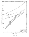
- FIG. 1 of the drawing shows the relationship between CTE and volume percent copper in an Invar-copper composite as effected by temperature of the hot rolling employed to make the composite sandwich of the invention.
- the range of volume percent copper in composites according to the invention is about 35-70 volume percent.
- FIG. 2 of the drawing For the sake of clarity, a composite of the invention is illustrated in Figure 2 of the drawing in exploded form and considerably exaggerated in proportion.
- the composite 11 overall comprises top layer of copper 13, bottom copper layer 15 sandwiching copper-Invar (or other low CTE alloy) plate 17.
- Plate 17 includes nickel-iron alloy matrix 19 and copper inserts 21.
- the copper layers 13 and 15 are bonded to and integral with the copper of copper inserts 21.
- Composite 11 is advantageously made by providing a perforated plate or sheet of nickel-iron alloy, sandwiching this sheet between two sheets of copper, raising the temperature of the sandwich to about 700 to about 950°C and hot rolling the sandwich to provide an integral composite as depicted in Figure 2.
- the composite of the invention could be made by electro- or electroless-plating of copper on a perforated plate or sheet of low CTE nickel-iron alloy followed by hot deforming the deposited copper (e.g. by rolling) to completely fill the holes in the perforated plate. It is also possible to provide the required amount of copper by a combination of plated copper and sheet form copper.
- Invar sheet containing 36% nickel, balance iron, along with the normal commercial impurities was rolled by conventional hot rolling procedures to strips 0.89 mm and 1.27 mm in thickness.
- the electrical resistivity of this strip was measured at 81 micro ohm cm.
- the CTE was measured at 2.0 ppm/°C between 30 and 400°C.
- Copper sheet of commercial grade was purchased in thicknesses of 0.38 mm, 0.508 mm and 0.635 mm.
- the electrical resistivity of this sheet was measured at 1.8 micro ohm cm and the CTE at 18 ppm/°C.
- the Invar strip was perforated with 1.59 mm diameter holes on 2.78 mm staggered centers to give a perforated Invar strip with 28% open area in it.
- the strips were cut into lengths and observed by metallographic methods. All of the holes in the Invar strip were completely filled with copper. The copper was integrally bound to the Invar even in the holes. The whole sandwich was flat and free of surface cracks.
- the longitudinal resistivity of the composite strips was calculated by first calculating the final thickness of the copper sheet after allowance for filling the holes in the Invar, then applying known simple standard equations using the previously measured resistivities of 1.8 micro ohm cm for the starting copper and 81 micro ohm cm for the starting Invar sheet.
- thermal conductivities of copper alloys are inversely proportional to the electrical resistivity.
- thermal conductivities are inversely proportional to the electrical resistivity.
- Calculated values of the thermal conductivity for the composites both in the plane of the composite or through the sheet are shown in Table I.
- CTE values for the Texas Instruments (TI) Cu/Invar/Cu sandwich made with a non-perforated sheet of Invar track the CTE values of the composite of the present invention very well based upon overall volume percent copper.
- the thermal conductivities of the TI composites in the x-y directions are roughly 10 times the thermal conductivities in the z direction.
- the CTE values of the TI composites are taken from the literature referenced at the start of this patent application. Our calculations show that in the composite as described and defined in U.S. Patent 4,283,464 the CTE is about 15 ppm/°C rather than 7 ppm/°C as reported and the thermal conductivity in the "z" direction is about 6 times the thermal conductivity in the "x-y" directions.
- CTE data for the composites of the present invention is plotted as a function of volume percent copper in Figure 1. Note that for the composite construction in the useful range of this invention, the CTE of the composite is a function only of the volume % Cu and the hot rolling temperature. Published data points relative to the CTE's of Texas Instruments composites fall on the same line as data points relative to composites of this invention hot rolled at 850°C. The difference in CTE between 750°C hot rolling and 850°C hot rolling is greater at greater percentages of copper because when the composite is rolled at the higher temperature the copper exerts a higher compressive force on the Invar as it cools.
- the present invention contemplates useful Cu/Invar/Cu composites hithertofore not constructed in which Invar sheet (36% Ni, bal. Fe) is perforated with small holes (0.79 to 1.59 mm in diameter) such that from about 15 to 40% of the volume of the Invar sheet is holes.
- the Invar sheet is then surrounded on each side by pure copper sheets.
- the thicknesses of the copper and Invar sheets are selected to provide volume percent of copper of from 20 to 60% and such that the thermal conductivity of the finished composite will be roughly isotropic.
- the three sheets of Cu/Invar/Cu are then heated from about 750 to about 900°C (preferably 850°C) in a reducing atmosphere then hot rolled.
- the rolling at temperature in the reducing atmosphere is highly preferred to ensure that the copper completely fills every hole and is integrally bonded to itself and to the Invar even on the sides of the punched holes.
- the resulting composite can be subsequently cold rolled to the final thickness desired.
- the conductivity of central Invar-Cu plate is then used to calculate the overall conductivity of the composite. While the foregoing calculation does not take into account interfacial barriers to thermal conductivity and is valid only in the temperature range in which the values of K Cu and K Invar are reasonable, it is believed that this calculation reasonably predicts the thermal conductivities of the composites of the present invention.
- Figure 3 shows the effect of Invar perforation on the conductivities both in the x-y (K x-y ) directions and the z direction (K z ) for three different copper-Invar combinations. Similar curves for any other copper-low-expansivity-alloy-copper combination could be plotted for both electrical and thermal conductivity.
- Curves A, B and C show the relationship between thermal conductivity in the z direction and the volume percentage of copper-filled through passages in inner copper-Invar plate 17.
- Curves A', B' and C' show the corresponding relationship with respect to thermal conductivity in the x-y directions.
- the thicknesses in mm of the layers in the respective composites are as follows:
Applications Claiming Priority (1)
| Application Number | Priority Date | Filing Date | Title |
|---|---|---|---|
| CA000587036A CA1316303C (en) | 1988-12-23 | 1988-12-23 | Composite structure |
Publications (1)
| Publication Number | Publication Date |
|---|---|
| EP0437656A1 true EP0437656A1 (de) | 1991-07-24 |
Family
ID=4139369
Family Applications (1)
| Application Number | Title | Priority Date | Filing Date |
|---|---|---|---|
| EP90100921A Ceased EP0437656A1 (de) | 1988-12-23 | 1990-01-17 | Mischstruktur mit spezifischem Wärmeausdehnungskoeffizienten |
Country Status (3)
| Country | Link |
|---|---|
| US (1) | US4996115A (de) |
| EP (1) | EP0437656A1 (de) |
| CA (1) | CA1316303C (de) |
Cited By (7)
| Publication number | Priority date | Publication date | Assignee | Title |
|---|---|---|---|---|
| EP0537965A2 (de) * | 1991-10-12 | 1993-04-21 | Sumitomo Special Metals Company Limited | Verfahren zur Herstellung eines warmleitenden Materials |
| DE4217531C1 (de) * | 1992-05-27 | 1993-12-16 | Wieland Werke Ag | Verfahren zur Herstellung schlickergegossener isotroper Verbundwerkstoffe auf Kupferbasis mit geringem thermischem Ausdehnungskoeffizienten und hoher elektrischer Leitfähigkeit sowie deren Verwendung |
| EP0661916A1 (de) * | 1993-07-06 | 1995-07-05 | Kabushiki Kaisha Toshiba | Wärmeabfuhrplatte |
| WO1998020548A1 (en) * | 1996-11-08 | 1998-05-14 | W.L. Gore & Associates, Inc. | Package for mounting an integrated circuit chip |
| WO1998020549A1 (en) * | 1996-11-08 | 1998-05-14 | W.L. Gore & Associates, Inc. | Use of variable perforation density in copper layer to control cte |
| FR2844097A1 (fr) * | 2002-08-27 | 2004-03-05 | Toyota Jidoshokki Kk | Plaque a faible dilatation, procede de fabrication de celle-ci et dispositif a semi-conducteur utilisant la plaque a faible dilatation |
| US6994917B2 (en) | 2003-01-15 | 2006-02-07 | Kabushiki Kaisha Toyota Jidoshokki | Composite material and method for manufacturing the same |
Families Citing this family (31)
| Publication number | Priority date | Publication date | Assignee | Title |
|---|---|---|---|---|
| US5015803A (en) * | 1989-05-31 | 1991-05-14 | Olin Corporation | Thermal performance package for integrated circuit chip |
| DE69211216T2 (de) * | 1991-03-27 | 1996-11-07 | Seb Sa | Formteil hergestellt aus einer verhältnismässig weichen Metallplatte und Kochgefäss mit einem solchen Formteil |
| US5156923A (en) * | 1992-01-06 | 1992-10-20 | Texas Instruments Incorporated | Heat-transferring circuit substrate with limited thermal expansion and method for making |
| US5296310A (en) * | 1992-02-14 | 1994-03-22 | Materials Science Corporation | High conductivity hydrid material for thermal management |
| US5608267A (en) * | 1992-09-17 | 1997-03-04 | Olin Corporation | Molded plastic semiconductor package including heat spreader |
| US5310520A (en) * | 1993-01-29 | 1994-05-10 | Texas Instruments Incorporated | Circuit system, a composite material for use therein, and a method of making the material |
| US5681663A (en) * | 1995-06-09 | 1997-10-28 | Ford Motor Company | Heatspreader carrier strip |
| JPH09312361A (ja) * | 1996-05-22 | 1997-12-02 | Hitachi Metals Ltd | 電子部品用複合材料およびその製造方法 |
| US5876831A (en) * | 1997-05-13 | 1999-03-02 | Lockheed Martin Corporation | High thermal conductivity plugs for structural panels |
| US6129993A (en) * | 1998-02-13 | 2000-10-10 | Hitachi Metals, Ltd. | Heat spreader and method of making the same |
| US6102112A (en) * | 1998-02-17 | 2000-08-15 | Lockheed Martin Corporation | Thermally conductive support structure |
| JP2000281802A (ja) * | 1999-03-30 | 2000-10-10 | Polymatech Co Ltd | 熱伝導性成形体およびその製造方法ならびに半導体装置 |
| US6075701A (en) * | 1999-05-14 | 2000-06-13 | Hughes Electronics Corporation | Electronic structure having an embedded pyrolytic graphite heat sink material |
| US6355364B1 (en) * | 1999-06-29 | 2002-03-12 | International Business Machines Corporation | Process of heat treating and annealing CIC and CIC created thereby |
| US6518509B1 (en) * | 1999-12-23 | 2003-02-11 | International Business Machines Corporation | Copper plated invar with acid preclean |
| ITMI20010807A1 (it) * | 2000-04-14 | 2002-10-13 | Saint Gobain | Procedimento per la fabbricazione di piste elettroconduttorici sunun substrato trasparente e substrato ottenuto |
| US20030131476A1 (en) * | 2001-09-28 | 2003-07-17 | Vlad Ocher | Heat conduits and terminal radiator for microcircuit packaging and manufacturing process |
| US7416789B2 (en) | 2004-11-01 | 2008-08-26 | H.C. Starck Inc. | Refractory metal substrate with improved thermal conductivity |
| US20060286358A1 (en) * | 2005-03-14 | 2006-12-21 | Tower Steven A | Heat spreader for use with light emitting diode |
| US7960032B2 (en) * | 2005-05-24 | 2011-06-14 | Demers Joseph R | High thermal conductivity, high yield strength, metal composite and method |
| US20080008217A1 (en) * | 2006-07-07 | 2008-01-10 | Newport Corporation | Laser device including heat sink with a tailored coefficient of thermal expansion |
| US20080008216A1 (en) * | 2006-07-07 | 2008-01-10 | Newport Corporation | Laser device including heat sink with insert to provide a tailored coefficient of thermal expansion |
| DE102007019885B4 (de) * | 2007-04-27 | 2010-11-25 | Wieland-Werke Ag | Kühlkörper mit matrixförmig strukturierter Oberfläche |
| US20090208722A1 (en) * | 2008-02-18 | 2009-08-20 | John Francis Timmerman | Oriented Members for Thermally Conductive Interface Structures |
| US7956446B2 (en) * | 2008-05-13 | 2011-06-07 | Infineon Technologies Ag | Semiconductor device and method |
| US8081468B2 (en) * | 2009-06-17 | 2011-12-20 | Laird Technologies, Inc. | Memory modules including compliant multilayered thermally-conductive interface assemblies |
| US20100321897A1 (en) * | 2009-06-17 | 2010-12-23 | Laird Technologies, Inc. | Compliant multilayered thermally-conductive interface assemblies |
| FR2951020B1 (fr) * | 2009-10-01 | 2012-03-09 | Nat De Metrologie Et D Essais Lab | Materiau composite multicouche utilise pour la fabrication de substrats de modules electroniques et procede de fabrication correspondant |
| JP2012138566A (ja) * | 2010-12-08 | 2012-07-19 | Nippon Dourooingu:Kk | 複合熱伝導部材 |
| US10611124B2 (en) * | 2015-10-06 | 2020-04-07 | Fourté International SDN. BHD | Multiple layered alloy/non alloy clad materials and methods of manufacture |
| US11032947B1 (en) * | 2020-02-17 | 2021-06-08 | Raytheon Company | Tailored coldplate geometries for forming multiple coefficient of thermal expansion (CTE) zones |
Citations (7)
| Publication number | Priority date | Publication date | Assignee | Title |
|---|---|---|---|---|
| FR2396263A1 (fr) * | 1977-06-29 | 1979-01-26 | Semi Alloys Inc | Plaque de transmission de la chaleur, metallique, composite et prefabriquee |
| GB2048567A (en) * | 1979-05-08 | 1980-12-10 | Hascoe N | Heat-transmitting plate unit |
| GB2074373A (en) * | 1980-03-27 | 1981-10-28 | Asea Ab | Composite material for intermediate phates for semiconductor devices |
| DE3144759A1 (de) * | 1980-11-21 | 1982-06-24 | General Electric Co., Schenectady, N.Y. | "waermespannungen beseitigende bimetallplatte" |
| FR2511193A1 (fr) * | 1981-08-07 | 1983-02-11 | Thomson Csf | Support en materiau colamine pour le refroidissement et l'encapsulation d'un substrat de circuit electronique |
| WO1988007422A1 (en) * | 1987-03-23 | 1988-10-06 | Olin Corporation | Low expansion copper alloys with high thermal conductivity |
| EP0332384A2 (de) * | 1988-03-10 | 1989-09-13 | Texas Instruments Incorporated | Schaltungssystem, zusammengesetztes Metallmaterial für dieses System und Verfahren zum Herstellen dieses Materials |
Family Cites Families (10)
| Publication number | Priority date | Publication date | Assignee | Title |
|---|---|---|---|---|
| US3175893A (en) * | 1959-02-02 | 1965-03-30 | Clevite Corp | Laminate composite material and method of fabrication |
| US3368122A (en) * | 1965-10-14 | 1968-02-06 | Gen Electric | Semiconductor devices |
| US3399332A (en) * | 1965-12-29 | 1968-08-27 | Texas Instruments Inc | Heat-dissipating support for semiconductor device |
| CH438497A (de) * | 1966-03-11 | 1967-06-30 | Bbc Brown Boveri & Cie | Halbleiteranordnung |
| US4025997A (en) * | 1975-12-23 | 1977-05-31 | International Telephone & Telegraph Corporation | Ceramic mounting and heat sink device |
| JPS603776B2 (ja) * | 1977-06-03 | 1985-01-30 | 株式会社日立製作所 | 半導体素子 |
| US4211354A (en) * | 1978-04-06 | 1980-07-08 | The United States Of America As Represented By The Administrator Of The National Aeronautics And Space Administration | Method for alleviating thermal stress damage in laminates |
| US4256792A (en) * | 1980-01-25 | 1981-03-17 | Honeywell Inc. | Composite electronic substrate of alumina uniformly needled through with aluminum nitride |
| JPS57130441A (en) * | 1981-02-06 | 1982-08-12 | Hitachi Ltd | Integrated circuit device |
| JPS5861677A (ja) * | 1981-10-09 | 1983-04-12 | Toshiba Corp | 半導体装置 |
-
1988
- 1988-12-23 CA CA000587036A patent/CA1316303C/en not_active Expired - Fee Related
-
1990
- 1990-01-17 EP EP90100921A patent/EP0437656A1/de not_active Ceased
- 1990-04-02 US US07/502,990 patent/US4996115A/en not_active Expired - Lifetime
Patent Citations (7)
| Publication number | Priority date | Publication date | Assignee | Title |
|---|---|---|---|---|
| FR2396263A1 (fr) * | 1977-06-29 | 1979-01-26 | Semi Alloys Inc | Plaque de transmission de la chaleur, metallique, composite et prefabriquee |
| GB2048567A (en) * | 1979-05-08 | 1980-12-10 | Hascoe N | Heat-transmitting plate unit |
| GB2074373A (en) * | 1980-03-27 | 1981-10-28 | Asea Ab | Composite material for intermediate phates for semiconductor devices |
| DE3144759A1 (de) * | 1980-11-21 | 1982-06-24 | General Electric Co., Schenectady, N.Y. | "waermespannungen beseitigende bimetallplatte" |
| FR2511193A1 (fr) * | 1981-08-07 | 1983-02-11 | Thomson Csf | Support en materiau colamine pour le refroidissement et l'encapsulation d'un substrat de circuit electronique |
| WO1988007422A1 (en) * | 1987-03-23 | 1988-10-06 | Olin Corporation | Low expansion copper alloys with high thermal conductivity |
| EP0332384A2 (de) * | 1988-03-10 | 1989-09-13 | Texas Instruments Incorporated | Schaltungssystem, zusammengesetztes Metallmaterial für dieses System und Verfahren zum Herstellen dieses Materials |
Cited By (15)
| Publication number | Priority date | Publication date | Assignee | Title |
|---|---|---|---|---|
| EP0537965A2 (de) * | 1991-10-12 | 1993-04-21 | Sumitomo Special Metals Company Limited | Verfahren zur Herstellung eines warmleitenden Materials |
| EP0537965A3 (en) * | 1991-10-12 | 1993-07-14 | Sumitomo Special Metals Co., Ltd. | Heat-conductive material and method of producing the same |
| DE4217531C1 (de) * | 1992-05-27 | 1993-12-16 | Wieland Werke Ag | Verfahren zur Herstellung schlickergegossener isotroper Verbundwerkstoffe auf Kupferbasis mit geringem thermischem Ausdehnungskoeffizienten und hoher elektrischer Leitfähigkeit sowie deren Verwendung |
| EP0579911A2 (de) * | 1992-05-27 | 1994-01-26 | Wieland-Werke Ag | Verfahren zur Herstellung schlickergegossener isotroper Verbundwerkstoffe auf Kupferbasis mit geringem thermischem Ausdehnungskoeffizienten und hoher elektrischer Leitfähigkeit sowie deren Verwendung |
| EP0579911A3 (en) * | 1992-05-27 | 1994-06-01 | Wieland Werke Ag | Process for preparing composite isotropic copper-based materials by slip casting, having a low thermal expansion coefficient and high electrical conductivity and their use |
| EP0661916A1 (de) * | 1993-07-06 | 1995-07-05 | Kabushiki Kaisha Toshiba | Wärmeabfuhrplatte |
| EP0661916A4 (de) * | 1993-07-06 | 1996-01-10 | Toshiba Kk | Wärmeabfuhrplatte. |
| US5660917A (en) * | 1993-07-06 | 1997-08-26 | Kabushiki Kaisha Toshiba | Thermal conductivity sheet |
| WO1998020548A1 (en) * | 1996-11-08 | 1998-05-14 | W.L. Gore & Associates, Inc. | Package for mounting an integrated circuit chip |
| WO1998020549A1 (en) * | 1996-11-08 | 1998-05-14 | W.L. Gore & Associates, Inc. | Use of variable perforation density in copper layer to control cte |
| US5900312A (en) * | 1996-11-08 | 1999-05-04 | W. L. Gore & Associates, Inc. | Integrated circuit chip package assembly |
| US6248959B1 (en) | 1996-11-08 | 2001-06-19 | W. L. Gore & Associates, Inc. | Substrate with die area having same CTE as IC |
| FR2844097A1 (fr) * | 2002-08-27 | 2004-03-05 | Toyota Jidoshokki Kk | Plaque a faible dilatation, procede de fabrication de celle-ci et dispositif a semi-conducteur utilisant la plaque a faible dilatation |
| US6994917B2 (en) | 2003-01-15 | 2006-02-07 | Kabushiki Kaisha Toyota Jidoshokki | Composite material and method for manufacturing the same |
| DE102004002030B4 (de) * | 2003-01-15 | 2009-06-10 | Kabushiki Kaisha Toyota Jidoshokki, Kariya | Verbundmaterial und Verfahren zu dessen Herstellung |
Also Published As
| Publication number | Publication date |
|---|---|
| US4996115A (en) | 1991-02-26 |
| CA1316303C (en) | 1993-04-20 |
Similar Documents
| Publication | Publication Date | Title |
|---|---|---|
| US4996115A (en) | Composite structure | |
| US7416789B2 (en) | Refractory metal substrate with improved thermal conductivity | |
| EP0537965B1 (de) | Verfahren zur Herstellung eines warmleitenden Materials | |
| US7570148B2 (en) | Low resistance polymer matrix fuse apparatus and method | |
| US5156923A (en) | Heat-transferring circuit substrate with limited thermal expansion and method for making | |
| US7436284B2 (en) | Low resistance polymer matrix fuse apparatus and method | |
| US4696851A (en) | Hybrid and multi-layer circuitry | |
| GB2048567A (en) | Heat-transmitting plate unit | |
| US6045927A (en) | Composite material for electronic part and method of producing same | |
| EP0365275B1 (de) | Kühlelement aus Verbundmaterial für ein Halbleiterbauelement und Herstellungsverfahren dafür | |
| US4771537A (en) | Method of joining metallic components | |
| GB2214933A (en) | Magnetic field shield including a superconductive film | |
| EP0392109A2 (de) | Wärmeleitendes zusammengesetztes Material | |
| JPH0738428B2 (ja) | 複合構造物 | |
| US4912284A (en) | Electrical circuits | |
| Radebaugh et al. | Flexible laminates for thermally grounded terminal strips and shielded electrical leads at low temperatures | |
| JPH05109947A (ja) | 熱伝導材料とその製造方法 | |
| KR940010910B1 (ko) | 반도체 패키지 | |
| JPH0322707B2 (de) | ||
| CA1193752A (en) | Electrical circuits | |
| JP3037485B2 (ja) | 熱伝導材料とその製造方法 | |
| Young et al. | Indirect bonding of Ni-electroless plated AlN and Cu by hot pressing method | |
| Klemencic et al. | Multilayer Circuit Boards with Molybdenum‐copper Metal Cores | |
| CN116157258A (zh) | 复合材料、散热器和半导体封装 | |
| Uribe et al. | Characterization of the mechanical properties of LTCC``Green Tape``{trademark} for the MC4352 MET |
Legal Events
| Date | Code | Title | Description |
|---|---|---|---|
| PUAI | Public reference made under article 153(3) epc to a published international application that has entered the european phase |
Free format text: ORIGINAL CODE: 0009012 |
|
| AK | Designated contracting states |
Kind code of ref document: A1 Designated state(s): AT BE CH DE DK ES FR GB GR IT LI LU NL SE |
|
| 17P | Request for examination filed |
Effective date: 19910902 |
|
| 17Q | First examination report despatched |
Effective date: 19931011 |
|
| STAA | Information on the status of an ep patent application or granted ep patent |
Free format text: STATUS: THE APPLICATION HAS BEEN REFUSED |
|
| 18R | Application refused |
Effective date: 19941208 |