EP0332384A2 - Schaltungssystem, zusammengesetztes Metallmaterial für dieses System und Verfahren zum Herstellen dieses Materials - Google Patents
Schaltungssystem, zusammengesetztes Metallmaterial für dieses System und Verfahren zum Herstellen dieses Materials Download PDFInfo
- Publication number
- EP0332384A2 EP0332384A2 EP89302238A EP89302238A EP0332384A2 EP 0332384 A2 EP0332384 A2 EP 0332384A2 EP 89302238 A EP89302238 A EP 89302238A EP 89302238 A EP89302238 A EP 89302238A EP 0332384 A2 EP0332384 A2 EP 0332384A2
- Authority
- EP
- European Patent Office
- Prior art keywords
- metal material
- percent
- composite metal
- copper
- discrete elements
- Prior art date
- Legal status (The legal status is an assumption and is not a legal conclusion. Google has not performed a legal analysis and makes no representation as to the accuracy of the status listed.)
- Withdrawn
Links
Images
Classifications
-
- H10W70/6875—
-
- H10W40/257—
-
- H—ELECTRICITY
- H05—ELECTRIC TECHNIQUES NOT OTHERWISE PROVIDED FOR
- H05K—PRINTED CIRCUITS; CASINGS OR CONSTRUCTIONAL DETAILS OF ELECTRIC APPARATUS; MANUFACTURE OF ASSEMBLAGES OF ELECTRICAL COMPONENTS
- H05K1/00—Printed circuits
- H05K1/02—Details
- H05K1/03—Use of materials for the substrate
- H05K1/05—Insulated conductive substrates, e.g. insulated metal substrate
-
- H10W72/5363—
-
- H10W72/5449—
-
- H10W72/884—
-
- H10W90/754—
-
- Y—GENERAL TAGGING OF NEW TECHNOLOGICAL DEVELOPMENTS; GENERAL TAGGING OF CROSS-SECTIONAL TECHNOLOGIES SPANNING OVER SEVERAL SECTIONS OF THE IPC; TECHNICAL SUBJECTS COVERED BY FORMER USPC CROSS-REFERENCE ART COLLECTIONS [XRACs] AND DIGESTS
- Y10—TECHNICAL SUBJECTS COVERED BY FORMER USPC
- Y10T—TECHNICAL SUBJECTS COVERED BY FORMER US CLASSIFICATION
- Y10T428/00—Stock material or miscellaneous articles
- Y10T428/12—All metal or with adjacent metals
- Y10T428/12486—Laterally noncoextensive components [e.g., embedded, etc.]
Definitions
- the field of this invention is that of semiconductor circuit systems and the invention relates more particularly to a composite metal material for use in mounting semiconductor devices in such systems.
- U.S. Patent No. 3,399,332 provides a grid of a metal material of relatively low coefficient of thermal expansion having openings in the grid filled with a copper material or the like of relatively higher thermal conductivity to provide a mounting for a semiconductor device having a desired combination of thermal expansion and conductivity properties.
- the patent suggests that particles of a ferrous alloy can be impregnated into a copper material for providing an alternate material having selected thermal expansion and conductivity properties.
- U.S. Patent No. 4,283,464 provides two grids of a metal material of relatively low coefficient of thermal expansion on either side of an inner layer of copper metal for providing a composite substrate material having another described combination of thermal expansion and conductivity properties.
- 4,472,672 shows layer combinations of ferrous metal materials of relatively low thermal expansion properties with layer materials of relatively high thermal conductivity where the layer thicknesses are regulated to be within selected ranges for providing composite metal materials with coefficients of thermal expansion substantially corresponding to those of semiconductor devices to be mounted thereon.
- 4,158,719 show composite metal materials formed by powder metallurgy techniques or the like either by compacting mixtures of metal powders of relatively low coefficient of thermal expansion with metal powders of relatively high thermal conductivity materials and then heating the compacted powders for diffusion bonding the particles to each other or by compacting and sintering one of the metal powders to form a porous sintered compact and by then filling the pores of that sintered compact with a melt of the other metal material.
- a composite metal material could be provided for use as a substrate in a semiconductor circuit system or if the composite metal material could be easily and economically manufactured and could be characterized by improved combination of thermal expansion and conductivity properties while also being characterized by improved malleability of the material for permitting easier application of the material in semiconductor circuit systems and the like.
- a plurality of discrete particles or elements of a ferrous metal alloy having a relatively low coefficient of thermal expansion are coated with a copper material having a relatively high thermal conductivity.
- particles of the ferrous alloy having a particle size in the range from about 44 microns to 425 microns are cleaned in conventional manner and are coated with a copper material in any conventional manner by electroplating or electroless copper plating or the like.
- the particles can be formed by cladding a fine core wire of the low expansion metal with copper and by then cutting short lengths from the wire to form the discrete elements, and if desired, the coated discrete elements can be mixed with other copper metal particles.
- coated particles or elements and/or other copper particles are then pressed together in accordance with conventional powder metallurgy techniques, preferably forming a compact having a porosity of less than about 40 percent or the like, and are heated for diffusion-bonding the copper coatings, or the copper-coated portions of the discrete elements, to each other to form a continuous copper matrix having the discrete elements secured in dispersed relation therein, the heating being regulated with respect to temperature and duration to be sufficient for diffusion-bonding the copper coatings to each other while substantially avoiding diffusion of ferrous constituents or the like from the discrete elements into the copper materials.
- the proportion of the discrete element materials provided in the composite metal material is easily regulated with respect to the proportion of the copper material therein by regulation of the plating process or by addition of copper powders to provide the composite metal material with a selected thermal expansion coefficient, preferably in the range from about 4 PPM/°C. to 8 PPM/°C.
- the coatings on the elements are also easily bonded together with each other, or with copper powders, in a reliable and secure manner for forming the desired composite metal material while retaining the high thermal conductivity characteristics of the copper material in the composite and without introducing any substantial diffusion of nickelous, ferrous, or other materials from the discrete elements into the copper materials such as would substantially reduce the thermal conductivity of the copper materials.
- the composite metal material is adapted to display substantial malleability and the semiconductor devices are easily mounted on substrates formed of the composite metal materials of this invention for providing improved semiconductor circuit systems.
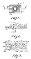
- 10 in Figure 1 indicates the novel and improved circuit systems of this invention which is shown to include a substrate 12 (not sectioned in Fig. 2) having a semiconductor device 14 such as a conventional integrated circuit chip or the like secured by a thermally and electrically conductive epoxy material or by a tin-lead solder material 13, or by an electrically conducting or nonconducting epoxy or the like, to the substrate.
- the substrate is selectively coated with an electrically insulating material 16 and has electrically conductive circuit paths 18 formed on the electrical insulating coating in any conventional manner, the semiconductor device having selected terminals 14.1 thereof electrically connected to selected circuit paths 18 on the substrate by wire-bond leads 20 or in any other conventional manner.
- the substrate 12 as best shown in Figure 3 comprises a composite metal material including a continuous matrix 22 of a first metal material having a plurality, and preferably a great multiplicity, of discrete elements 24 of other metal materials secured in dispersed relation therein.
- the discrete elements embody ferrous metal materials having relatively low coefficient of thermal expansion relative to the noted matrix material for cooperating with the continuous matrix material to provide the composite metal material 12 with a selected coefficient of thermal expansion which is relatively much lower than the thermal expansion properties of the continuous matrix material.
- the continuous matrix material 22 comprises a copper material having a relatively high thermal conductivity characteristic as compared to the materials of the discrete elements 24 and the matrix material is substantially free of ferrous metal or other alloying constituents such as might tend to lower the thermal conductivity of the copper matrix material.
- the discrete elements 24 are dispersed throughout the composite metal material and define a plurality of relatively high heat conductivity paths which are both serpentine and/or direct as indicated at 26 in Figure 3 passing between the plate surfaces 12.1 and 12.2 of the composite metal material.
- the size of the discrete elements is such that the thickness of the composite metal material between surfaces 12.1 and 12.2 accommodates many of the particles or discrete elements 24 along a path between those surfaces, approximately 4 being shown in Figure 3.
- the discrete elements 24 preferably comprise particles of ferrous metal alloys selected from a group consisting of alloys having nominal compositions by weight of about 36 to 50 percent nickel and the balance iron, of about 31 percent nickel, 8 percent chromium, 8 percent cobalt and the balance iron, of about 32 percent nickel, 15 percent cobalt, 1 percent molybdenum and the balance iron, of about 38 percent nickel, 7 percent chromium and the balance iron, of about 17 percent chromium and the balance iron, of about 16.5 percent chromium, 4.5 percent aluminum and the balance iron, of about 57 percent cobalt, 9 percent chromium and the balance iron, and of about 23 to 30 percent nickel, about 17 to 30 percent cobalt, about 0.6 to 0.8 percent manganese and the balance iron.
- ferrous metal alloys selected from a group consisting of alloys having nominal compositions by weight of about 36 to 50 percent nickel and the balance iron, of about 31 percent nickel, 8 percent chromium, 8 percent cobalt and the balance iron, of about 32 percent
- Such discrete element particles are preferably formed in any conventional manner by atomizing or the like and are provided with particle sizes in the range from 44 to 425 micron diameter for providing the composite metal material 12 with desired malleability.
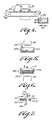
- the particles are deposited as diagrammatically indicated at 27 in Figure 4 on a carrier mechanism as is diagrammatically illustrated at 28 in Figure 4 to be advanced for cleaning the particles in any conventional manner.
- the particles are advanced through an oven diagrammatically indicated at 30 in Figure 4 wherein the particles are cleaned by heating as indicated at 32 in a reducing atmosphere of hydrogen or the like indicated at 34 for removing surface oxides and greases and the like from the particles.
- the particles are cleaned in any other conventional manner in accordance with this invention.
- the particles 24 are then introduced into an electroless copper plating bath 36 for a selected period of time for coating the particles 24 with a copper material 22 a or the like as shown in Figure 4.
- a conventional aqueous electroless copper plating bath 36 is prepared comprising metal salts and reducing agents in water at a temperature on the order of 25 to 70°C. in concentration of about 15 grams per liter.
- the particles 24 are introduced into the bath in a container 38 by means of a screen basket or the like (not shown) and are agitated thereon as indicated by arrow 40 in Figure 4 for 30-80 minutes to provide the particles 24 with coatings 22 a corresponding in volume to about 30 to 50 percent of the volume of the coated particles.
- the particles are preferably introduced into the bath at a temperature of about 25° C. and the bath is continuously supplemented to maintain the concentration of the bath as the particles are plated therein, whereby the particles are each coated with a desired copper material around all surfaces of the particles.
- the copper coating provided on the particles preferably comprises a copper material such as a substantially pure copper or the like preferably having a thermal conductivity on the order of about 9.9 watts/in./°C.
- the method for electroless copper plating the particles herein is conventional it is not further described herein and it will be understood that any conventional electroless copper plating of the particles 24 is within the scope of this invention.
- the copper coating 22 a of the particles 24 as provided in the bath indicated at 36 in Figure 4 are applied by electrolytic plating of the particles or in any other conventional manner.
- the discrete particles 24 with the coatings 22 a are dried by brief heating or the like as diagrammatically indicated at 42 in Figure 5 and/or by blow drying or the like as diagrammatically indicated at 44 in Figure 5.
- the dry, coated particles are then pressed together by pressing means 45, preferably with a force in the range from 2,000 to 100,000 psi or the like, in any conventional manner commonly employed in powder metallurgy to form a compact 12 a as indicated in Figure 6, the powder compact then being heated in any conventional manner as diagrammatically indicated at 48 in Figure 6 for diffusion-bonding copper coatings 22 a of the particles along interfaces as indicated at 22 b in Figure 3 to form the continuous copper matrix 22 having the discrete particles or elements 24 secured in dispersed relation therein.
- the heating for this diffusion-bonding is regulated to be adequate for accomplishing the desired diffusion-bonding of the copper coatings to each other while leaving the copper materials of the coatings substantially free of diffusion of ferrous metal constituents from the materials of the discrete particles into the copper such as might significantly reduce the thermal conductivity of the copper materials below about 70 percent of pure copper or about 7 watts/in./° C.
- the thermal conductivity of the copper is retained at 8 watts/in./°C. or better.
- the copper coatings 22 a formed on the discrete elements 24 constitute from about 30 to 50 percent of the volume of the coated particles so that the continuous copper matrix 22 formed in the composite metal material comprises from 30 to 50 percent of the volume of the composite material.
- the materials and the coating thicknesses of the coated particles are selected so that the materials of the particles and the coatings cooperate in providing the composite metal material 12 with a coefficient of thermal expansion in the range from about 4 PPM/°C. to 8 PPM/°C. and with an effective thermal conductivity between surfaces 12.1 and 12.2 of the composite metal material in the range from about 2.5 watts/in./°C. to about 5.0 watts/in/°C.
- the discrete particles 24 comprise a ferrous metal alloy having a nominal composition by weight of 36 percent nickel and the balance iron and are provided in a size range from 45 to 425 microns.
- the particles are cleaned by reduction in hydrogen and are electroless copper plated as in the bath noted above for providing the particles with copper coating constituting 40 percent of the volume of the coated particles.
- the particles are blown dry in nitrogen and compacted in conventional manner with a force of 2,000 to 100,000 psi or the like to form a compact having a porosity of less than about 40 percent and are heated to a temperature of less than about 850°C., and preferably to a temperature in the range from 600 to about 850°C., for 1 to 20 minutes to form a substantially pore-free composite metal material 12 having a continuous copper matrix 22 substantially free of ferrous metal diffusions therein from the discrete elements.
- the composite metal material will display a coefficient of thermal expansion on the order of 7 PPM/°C. and a thermal conductivity on the order of 3.5 watt/in./°C. and will display substantial malleability for permitting rolling reduction of the thickness of the composite metal materials, preferably in the range from 0.005 to 0.060 inches, to facilitate application of the composite metal materials in making substrates for circuit systems 10 as above described.
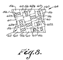
- a plurality or multiplicity of those discrete elements corresponding in many respects to the discrete elements 24 previously described are then cleaned if desired, are compacted together with each other with or without addition of other copper metal powder 60 and are heated in the manner previously described so that the copper coating surfaces of the discrete elements 56 and the copper powder are diffusion-bonded together with each other for forming a continuous copper matrix 62 and for securing the discrete element cores 56.1 in dispersed relation therein to form the composite metal material 64, the cores cooperating with the copper matrix in providing the composite metal material with an effective coefficient of thermal expansion relatively much lower than that of the copper material as above described.
- the heating for diffusion-bonding is regulated to be high enough to diffusion-bond the copper coatings to each other, and to the copper powders if used, along the interfaces indicated at 62 a in Figure 8 for forming a substantially pore-free composite metal while substantially avoiding diffusion of nickel, iron or other materials from the core elements 56.1 into the copper materials such that the copper materials themselves preferably retain a thermal conductivity on the order of 8 watts/in./°C. or better or described above while also achieving desired effective thermal expansion coefficients in the composite material.
Landscapes
- Cooling Or The Like Of Semiconductors Or Solid State Devices (AREA)
- Chemically Coating (AREA)
- Conductive Materials (AREA)
- Powder Metallurgy (AREA)
Applications Claiming Priority (2)
| Application Number | Priority Date | Filing Date | Title |
|---|---|---|---|
| US07/166,290 US4894293A (en) | 1988-03-10 | 1988-03-10 | Circuit system, a composite metal material for use therein, and a method for making the material |
| US166290 | 1988-03-10 |
Publications (2)
| Publication Number | Publication Date |
|---|---|
| EP0332384A2 true EP0332384A2 (de) | 1989-09-13 |
| EP0332384A3 EP0332384A3 (de) | 1990-08-29 |
Family
ID=22602637
Family Applications (1)
| Application Number | Title | Priority Date | Filing Date |
|---|---|---|---|
| EP89302238A Withdrawn EP0332384A3 (de) | 1988-03-10 | 1989-03-06 | Schaltungssystem, zusammengesetztes Metallmaterial für dieses System und Verfahren zum Herstellen dieses Materials |
Country Status (3)
| Country | Link |
|---|---|
| US (1) | US4894293A (de) |
| EP (1) | EP0332384A3 (de) |
| JP (1) | JPH029155A (de) |
Cited By (8)
| Publication number | Priority date | Publication date | Assignee | Title |
|---|---|---|---|---|
| EP0437656A1 (de) * | 1988-12-23 | 1991-07-24 | Inco Limited | Mischstruktur mit spezifischem Wärmeausdehnungskoeffizienten |
| WO1991013462A3 (en) * | 1990-02-23 | 1991-10-17 | Lanxide Technology Co Ltd | Methods of forming electronic packages |
| EP0411286B1 (de) * | 1989-08-03 | 1994-12-28 | International Business Machines Corporation | Wärmeleitpaste mit Flüssigmetallmatrix |
| US5526867A (en) * | 1988-11-10 | 1996-06-18 | Lanxide Technology Company, Lp | Methods of forming electronic packages |
| EP0840654A4 (de) * | 1994-11-14 | 2002-02-06 | Alan F Beane | Herstellung von partikeln und artikeln mit modifizierten eigenschaften |
| EP1296372A3 (de) * | 2001-09-21 | 2006-07-26 | Kabushiki Kaisha Toyota Jidoshokki | Hitzeableitmaterial und seine Herstellungsmethode |
| WO2008008939A3 (en) * | 2006-07-13 | 2008-02-28 | Parker Hannifin Corp | Emi absorbing gap filling material |
| KR20180067843A (ko) * | 2016-12-13 | 2018-06-21 | 서울대학교산학협력단 | 저열팽창 고열전도 복합재 및 이의 제조방법 |
Families Citing this family (20)
| Publication number | Priority date | Publication date | Assignee | Title |
|---|---|---|---|---|
| US5015533A (en) * | 1988-03-10 | 1991-05-14 | Texas Instruments Incorporated | Member of a refractory metal material of selected shape and method of making |
| US5050040A (en) * | 1988-10-21 | 1991-09-17 | Texas Instruments Incorporated | Composite material, a heat-dissipating member using the material in a circuit system, the circuit system |
| US5443615A (en) * | 1991-02-08 | 1995-08-22 | Honda Giken Kogyo Kabushiki Kaisha | Molded ceramic articles |
| US5215350A (en) * | 1991-03-20 | 1993-06-01 | Tachi-S Co., Ltd. | Lumbar support device |
| US5292478A (en) * | 1991-06-24 | 1994-03-08 | Ametek, Specialty Metal Products Division | Copper-molybdenum composite strip |
| US5614320A (en) * | 1991-07-17 | 1997-03-25 | Beane; Alan F. | Particles having engineered properties |
| US5156923A (en) * | 1992-01-06 | 1992-10-20 | Texas Instruments Incorporated | Heat-transferring circuit substrate with limited thermal expansion and method for making |
| US5310520A (en) * | 1993-01-29 | 1994-05-10 | Texas Instruments Incorporated | Circuit system, a composite material for use therein, and a method of making the material |
| AU715872B2 (en) * | 1995-07-27 | 2000-02-10 | Alan F. Beane | Manufacturing particles and articles having engineered properties |
| US6132676A (en) * | 1997-06-30 | 2000-10-17 | Massachusetts Institute Of Technology | Minimal thermal expansion, high thermal conductivity metal-ceramic matrix composite |
| US6897603B2 (en) * | 2001-08-24 | 2005-05-24 | Si Diamond Technology, Inc. | Catalyst for carbon nanotube growth |
| US20080165442A1 (en) * | 2006-11-08 | 2008-07-10 | Wenshan Cai | System, method and apparatus for cloaking |
| JP5577356B2 (ja) * | 2009-02-17 | 2014-08-20 | アプライド ナノストラクチャード ソリューションズ リミテッド ライアビリティー カンパニー | カーボン・ナノチューブを繊維上に含んで構成された複合材料 |
| US20110123735A1 (en) * | 2009-11-23 | 2011-05-26 | Applied Nanostructured Solutions, Llc | Cnt-infused fibers in thermoset matrices |
| US20110124253A1 (en) * | 2009-11-23 | 2011-05-26 | Applied Nanostructured Solutions, Llc | Cnt-infused fibers in carbon-carbon composites |
| AU2010350689A1 (en) * | 2009-11-23 | 2012-04-19 | Applied Nanostructured Solutions, Llc | CNT-tailored composite land-based structures |
| US8545963B2 (en) * | 2009-12-14 | 2013-10-01 | Applied Nanostructured Solutions, Llc | Flame-resistant composite materials and articles containing carbon nanotube-infused fiber materials |
| AU2011256789A1 (en) * | 2010-02-02 | 2012-07-12 | Applied Nanostructured Solutions, Llc | Fiber containing parallel-aligned carbon nanotubes |
| US9017854B2 (en) | 2010-08-30 | 2015-04-28 | Applied Nanostructured Solutions, Llc | Structural energy storage assemblies and methods for production thereof |
| US20120280430A1 (en) * | 2011-05-05 | 2012-11-08 | Applied Nanostructured Solutions, Llc | Composite tooling containing carbon nanotubes and production of parts therefrom |
Family Cites Families (15)
| Publication number | Priority date | Publication date | Assignee | Title |
|---|---|---|---|---|
| NL264799A (de) * | 1960-06-21 | |||
| US3220107A (en) * | 1961-03-06 | 1965-11-30 | Texas Instruments Inc | Manufacture of clad rods, tubing and clad tubing |
| US3399332A (en) * | 1965-12-29 | 1968-08-27 | Texas Instruments Inc | Heat-dissipating support for semiconductor device |
| US4158719A (en) * | 1977-06-09 | 1979-06-19 | Carpenter Technology Corporation | Low expansion low resistivity composite powder metallurgy member and method of making the same |
| JPS5593230A (en) * | 1979-01-10 | 1980-07-15 | Toshiba Corp | Soldering method for semiconductor device |
| US4283464A (en) * | 1979-05-08 | 1981-08-11 | Norman Hascoe | Prefabricated composite metallic heat-transmitting plate unit |
| SE420964B (sv) * | 1980-03-27 | 1981-11-09 | Asea Ab | Kompositmaterial och sett for dess framstellning |
| JPS5946050A (ja) * | 1982-09-09 | 1984-03-15 | Narumi China Corp | 半導体用セラミツクパツケ−ジ |
| US4472672A (en) * | 1982-12-13 | 1984-09-18 | Motorola Inc. | High power factor switching-type battery charger |
| JPS59141248A (ja) * | 1983-01-31 | 1984-08-13 | Sumitomo Electric Ind Ltd | 半導体基板材料 |
| US4529836A (en) * | 1983-07-15 | 1985-07-16 | Sperry Corporation | Stress absorption matrix |
| JPH061787B2 (ja) * | 1983-09-20 | 1994-01-05 | 住友電気工業株式会社 | 半導体装置用基板 |
| US4569692A (en) * | 1983-10-06 | 1986-02-11 | Olin Corporation | Low thermal expansivity and high thermal conductivity substrate |
| JPS62272558A (ja) * | 1986-05-20 | 1987-11-26 | Sumitomo Electric Ind Ltd | 半導体装置用基板の製造方法 |
| US4822693A (en) * | 1987-03-23 | 1989-04-18 | Olin Corporation | Copper-iron-nickel composite material for electrical and electronic applications |
-
1988
- 1988-03-10 US US07/166,290 patent/US4894293A/en not_active Expired - Fee Related
-
1989
- 1989-03-06 EP EP89302238A patent/EP0332384A3/de not_active Withdrawn
- 1989-03-09 JP JP1057660A patent/JPH029155A/ja active Pending
Cited By (11)
| Publication number | Priority date | Publication date | Assignee | Title |
|---|---|---|---|---|
| US5163499A (en) * | 1988-11-10 | 1992-11-17 | Lanxide Technology Company, Lp | Method of forming electronic packages |
| US5526867A (en) * | 1988-11-10 | 1996-06-18 | Lanxide Technology Company, Lp | Methods of forming electronic packages |
| EP0437656A1 (de) * | 1988-12-23 | 1991-07-24 | Inco Limited | Mischstruktur mit spezifischem Wärmeausdehnungskoeffizienten |
| EP0411286B1 (de) * | 1989-08-03 | 1994-12-28 | International Business Machines Corporation | Wärmeleitpaste mit Flüssigmetallmatrix |
| WO1991013462A3 (en) * | 1990-02-23 | 1991-10-17 | Lanxide Technology Co Ltd | Methods of forming electronic packages |
| AU651822B2 (en) * | 1990-02-23 | 1994-08-04 | Lanxide Corporation | Methods of forming electronic packages |
| EP0840654A4 (de) * | 1994-11-14 | 2002-02-06 | Alan F Beane | Herstellung von partikeln und artikeln mit modifizierten eigenschaften |
| EP1296372A3 (de) * | 2001-09-21 | 2006-07-26 | Kabushiki Kaisha Toyota Jidoshokki | Hitzeableitmaterial und seine Herstellungsmethode |
| WO2008008939A3 (en) * | 2006-07-13 | 2008-02-28 | Parker Hannifin Corp | Emi absorbing gap filling material |
| GB2454837A (en) * | 2006-07-13 | 2009-05-27 | Parker Hannifin Corp | Emi absorbing gap filling material |
| KR20180067843A (ko) * | 2016-12-13 | 2018-06-21 | 서울대학교산학협력단 | 저열팽창 고열전도 복합재 및 이의 제조방법 |
Also Published As
| Publication number | Publication date |
|---|---|
| EP0332384A3 (de) | 1990-08-29 |
| JPH029155A (ja) | 1990-01-12 |
| US4894293A (en) | 1990-01-16 |
Similar Documents
| Publication | Publication Date | Title |
|---|---|---|
| US4894293A (en) | Circuit system, a composite metal material for use therein, and a method for making the material | |
| US5050040A (en) | Composite material, a heat-dissipating member using the material in a circuit system, the circuit system | |
| EP2617515B1 (de) | Klebematerial für halbleiterbauelemente | |
| JP4985129B2 (ja) | 接合体および電子モジュールならびに接合方法 | |
| EP0097058B1 (de) | Gesinterter Gegenstand aus Siliciumcarbid mit metallisierter Schicht und Verfahren zu seiner Herstellung | |
| US5358795A (en) | Heat-conductive material and method of producing the same | |
| EP0698590B1 (de) | Metallisierung von keramischen Materialien durch Auftrag einer haftenden reduzierbaren Schicht | |
| EP0797247A1 (de) | Substrat, auf dem Kontakthöcker aufgebildet sind und Herstellungsverfahren | |
| US5310520A (en) | Circuit system, a composite material for use therein, and a method of making the material | |
| CA2118758C (en) | Lead frame for integrated circuits | |
| KR101284363B1 (ko) | 금속코어 솔더볼 및 이를 이용한 반도체 장치의 방열접속구조 | |
| EP0365275B1 (de) | Kühlelement aus Verbundmaterial für ein Halbleiterbauelement und Herstellungsverfahren dafür | |
| US4659404A (en) | Method of making low thermal expansivity and high thermal conductivity substrate | |
| US11876030B2 (en) | Clad material and method for producing same | |
| JPH028334A (ja) | 複合材料及びその製造方法 | |
| EP3290399B1 (de) | Verfahren zum herstellen eines metall-keramik-substrats mit mindestens einem via | |
| EP1278404B1 (de) | Leiterplatte und verfahren zu ihrer herstellung | |
| JPH06268117A (ja) | 半導体装置用放熱基板およびその製造方法 | |
| US4407860A (en) | Process for producing an improved quality electrolessly deposited nickel layer | |
| CA1334132C (en) | Manufacture of low expansion composites having high electrical and heat conductivity | |
| JP3501366B2 (ja) | バイア充てん用導電性接着剤およびそれを用いた電子装置の製造方法 | |
| US4842959A (en) | Aluminum enamel board | |
| JPH05238857A (ja) | 窒化アルミニウム基板のメタライズ方法 | |
| JPH10163404A (ja) | Bga用入出力端子 | |
| EP3509403B1 (de) | Leiterplatte und verfahren zur herstellung davon |
Legal Events
| Date | Code | Title | Description |
|---|---|---|---|
| PUAI | Public reference made under article 153(3) epc to a published international application that has entered the european phase |
Free format text: ORIGINAL CODE: 0009012 |
|
| AK | Designated contracting states |
Kind code of ref document: A2 Designated state(s): DE FR GB IT NL |
|
| PUAL | Search report despatched |
Free format text: ORIGINAL CODE: 0009013 |
|
| AK | Designated contracting states |
Kind code of ref document: A3 Designated state(s): DE FR GB IT NL |
|
| 17P | Request for examination filed |
Effective date: 19910214 |
|
| 17Q | First examination report despatched |
Effective date: 19930608 |
|
| STAA | Information on the status of an ep patent application or granted ep patent |
Free format text: STATUS: THE APPLICATION IS DEEMED TO BE WITHDRAWN |
|
| 18D | Application deemed to be withdrawn |
Effective date: 19931019 |